Note: Descriptions are shown in the official language in which they were submitted.
3 CA 02939318 2016-08-10
DESCRIPTION
TITLE OF THE INVENTION:
HARD COATING FILM AND METHOD OF FORMING SAME
TECHNICAL FIELD
[0001]
The present invention relates to a hard film formed on a substrate surface of
a
tool such as a cutting tool or a die, particularly a tool formed of a non-
ferrous metal
material, and a method for manufacturing the same.
BACKGROUND ART
[0002]
In order to improve wear resistance in cutting and the like, a hard film
formed
of, for example, TiB2 or the like is commonly formed on a surface of a
substrate of a
tool. Then, technologies for forming such hard films are disclosed in Patent
Documents 1 to 4.
[0003]
Patent Document 1 discloses a cutting tool insert including a substrate and a
film containing at least one TiB2 layer. Further, Patent Document 2 discloses
a cutting
tool in which a hard covering layer is formed by vapor deposition on a surface
of a tool
substrate formed of a cubic boron nitride-based material sintered under an
ultrahigh
pressure, and discloses that the hard film layer is composed of a lower layer
formed of a
TiB2 layer, an intermediate layer formed of a two-phase mixed layer of a TiB2
layer and
a TiN layer, and an upper layer formed of a complex nitride layer of Ti and
Al. -
[0004]
Patent Document 3 discloses a film made by laminating a layer A composed of
a metal boride and a layer B containing carbon on each other. Further, Patent
Document 4 discloses a laminate including a laminated part formed of at least
two kinds
of compound layers mainly composed of one or more first elements selected from
the
group 4a, 5a and 6a elements in the periodic table, Al, Si and B, and one or
more second
elements selected from B, C, N and 0, and an intermediate layer composed of
one or
1
CA 02939318 2016-08-10
more third elements selected from the group 4a, 5a and 6a elements in the
periodic table
and one or more fourth elements selected from C, N and 0.
PRIOR ART DOCUMENTS
PATENT DOCUMENTS
[0005]
Patent Document 1: JP-A-2002-355704
Patent Document 2: JP-A-2010-228032
Patent Document 3: JP-A-2009-79266
Patent Document 4: JP-A-H08-127862
SUMMARY OF THE INVENTION
PROBLEMS THAT THE INVENTION IS TO SOLVE
[0006]
However, in the cutting tool insert of Patent Document 1, the film formed on
the substrate formed of a cemented carbide and the like contains the TiB2
layer. The
TiB2 layer is different from the substrate in crystal structure, so that
adhesion thereof to
the substrate is liable to be decreased. For this reason, the film described
in Patent
Document 1 has a problem of having inferior adhesion during cutting and the
like.
[0007]
In the cutting tool of Patent Document 2, the upper layer of the hard film
layer
acting as a working surface in cutting and the like has a composition of
TiAIN. The
film having the composition of TiAlN is easy to wear in cutting and the like
of a non-
ferrous metal material. For this reason, the hard covering layer described in
Patent
Document 2 has a problem of having inferior wear resistance during cutting and
the
like.
[0008]
In the film of Patent Document 3, the film is formed of the metal boride and
the carbide, and the metal boride and the carbide are low in adhesion to the
substrate
formed of a cemented carbide and the like. For this reason, the film
described in
Patent Document 3 has a problem of having inferior adhesion during cutting and
the
like.
2
CA 02939318 2016-08-10
[0009]
In the laminate of Patent Document 4, the laminated part acting as a working
surface in cutting and the like has a composition of TiN or AIN. The film
having the
composition of TiN or AIN is easy to wear in cutting and the like. For this
reason, the
laminate described in Patent Document 4 has a problem of having inferior wear
resistance during cutting and the like.
[0010]
The present invention has been made in view of the above-mentioned situation,
and objects thereof are to provide a hard film formed on a substrate surface
of a tool,
having high film hardness and having excellent adhesion and wear resistance
during
cutting and the like, and to provide a method for forming the same.
MEANS FOR SOLVING THE PROBLEMS
[0011]
The hard film in the present invention in order to solve the problems is a
hard
film to be formed on a substrate, the hard film including: a layer A having a
composition of Ti,(BõC 1 -x-yNy)1 -w satisfying0.20.6, irJ_y_0.5 and
y5_0.5; and a layer B having a composition of any one of Tii_aAla(Ci-kNk),
AlbCri-b(Ci-
kNk), Tii-c-d-eCreAldSie(Ci-kNk) and Tii_fSit(Ci_kNk), which satisfies
0.3a5_0.7,
0.050.3 and 0.51(..1, wherein
an underlying layer formed of the layer B is formed on the substrate, and an
adhesion
reinforcing layer in which the layers A and the layers B are alternately
repeatedly
laminated on one another is formed on the underlying layer, and
the layer A is increased in thickness compared to that on the underlying layer
side with an increase in thickness of the adhesion reinforcing layer, and a
maximum
thickness of the layer A is 20 to 50 nm.
[0012]
The above-mentioned hard film includes the layer A and the layer B each
having the predetermined composition, thereby increasing hardness of the hard
film and
improving wear resistance of the hard film. Further, the above-mentioned hard
film
includes the underlying layer formed of the layer B, thereby improving
adhesion
between the film and the substrate. Furthermore, the above-mentioned hard film
3
CA 02939318 2016-08-10
includes the adhesion reinforcing layer in which the layers A and the layers B
are
alternately repeatedly laminated on one another, the layer A is increased in
thickness
compared to that on the underlying layer side with an increase in the
thickness of the
adhesion reinforcing layer, and the maximum thickness thereof reaches the
predetermined thickness, thereby improving the adhesion of the hard film and
improving cutting performance to improve the wear resistance.
[0013]
In the hard film in the present invention, it is preferred that a layer C is
further
formed on the above-mentioned adhesion reinforcing layer, and the above-
mentioned
layer C having a composition of TiB2, and the thickness of the above-mentioned
layer C
is 5.0 pm or less. The above-mentioned hard film includes the layer C composed
of
TiB2, and thickness of the layer C is adjusted to the predetermined range,
thereby
preventing breakage (chipping) of the hard film and improving the wear
resistance of
the hard film.
[0014]
The first method for forming the hard film in the present invention includes:
a
substrate preparation step of preparing the substrate; a substrate heating
step of heating
the substrate; and a film forming step of forming the hard film on the
substrate, and in
the film forming step, the underlying layer and the adhesion reinforcing layer
are
formed by at least one of an arc ion plating process and a sputtering process.
[0015]
In the above-mentioned first method for forming the hard film, the film
forming step is performed by at least one of the arc ion plating process and
the
sputtering process, thereby forming the hard film including the underlying
layer formed
of the layer B having the predetermined composition and the adhesion
reinforcing layer
in which the layers A having the predetermined composition and the layers B
having the
predetermined composition are alternately repeatedly laminated on one another.
This
increases the hardness of the hard film and improves the wear resistance of
the hard
film. Further, in the first method for forming the hard film, the layer A is
formed in a
state where a predetermined bias voltage is applied on the substrate, thereby
improving
the wear resistance of the hard film.
[0016]
4
CA 02939318 2016-08-10
The second method for forming the hard film in the present invention includes:
a substrate preparation step of preparing the substrate; a substrate heating
step of
heating the substrate; and a film forming step of forming the hard film on the
substrate,
and in the film forming step, the underlying layer, the adhesion reinforcing
layer and the
layer C are formed by at least one of an arc ion plating process and a
sputtering process.
[0017]
In the above-mentioned second method for forming the hard film, the film
forming step is performed by at least one of the arc ion plating process and
the
sputtering process, thereby forming the hard film including the underlying
layer formed
of the layer B having the predetermined composition, the adhesion reinforcing
layer in
which the layers A having the predetermined composition and the layers B
having the
predetermined composition are alternately repeatedly laminated on one another,
and the
layer C composed of TiB2. This increases the hardness of the hard film and
improves
the wear resistance of the hard film. Further, in the second method for
forming the
hard film, the layer A and the layer C are formed in a state where a
predetermined bias
voltage is applied on the substrate, thereby improving the wear resistance of
the hard
film.
ADVANTAGEOUS EFFECTS OF THE INVENTION
[0018]
In the hard film of the present invention, it is formed on a substrate surface
of a
tool, and has high film hardness and excellent adhesion and wear resistance
during
cutting and the like. Further, in the forming method of the hard film of the
present
invention, the hard film having high hardness and excellent adhesion and wear
resistance during cutting and the like can be formed.
BRIEF DESCRIPTION OF THE DRAWINGS
[0019]
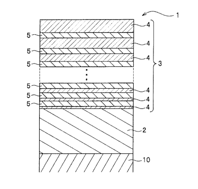
[FIG. 1] FIG. 1 is a cross-sectional view showing a first embodiment of a
hard film in the present invention.
[FIG. 2] FIG. 2 is a cross-sectional view showing a second embodiment of a
hard film in the present invention.
CA 02939318 2016-08-10
[FIG. 3] FIG. 3 is a diagram schematically illustrating a film deposition
apparatus.
MODE FOR CARRYING OUT THE INVENTION
[0020]
A first embodiment of a hard film in the present invention will be described
with reference to the drawing.
As shown in FIG. 1, a hard film 1 is a film formed on a substrate 10 for
improving adhesion and wear resistance, and includes an underlying layer 2 and
an
adhesion reinforcing layer 3 formed on the underlying layer 2.
[0021]
<Substrate>
Examples of the substrates 10 include cemented carbides, iron-based alloys,
cermets, high-speed tool steels and the like. However, the substrates 10
should not be
limited thereto, and may be tools such as cutting tools such as chips, drills
and end
mills, press dies, forging dies, molding dies and blanking punches.
[0022]
<Underlying layer>
The underlying layer 2 is a film formed on the substrate 10, and is formed of
a
layer B having a predetermined composition. The adhesion between the substrate
10
and the hard film 1 is improved by the formation of the underlying layer 2.
For this
reason, the thickness of the underlying layer 2 is preferably from 0.1 to 5
gm. The
details of the composition of the layer B will be described later.
[0023]
<Adhesion reinforcing layer>
The adhesion reinforcing layer 3 is a film formed on the underlying layer 2,
and is formed by alternately repeatedly laminating layers A 4 having a
predetermined
composition and layers B 5 having a predetermined composition on one another.
Then, the layer A 4 is increased in thickness compared to that on the
underlying layer 2
side with an increase in the thickness of the adhesion reinforcing layer 3,
and the
adhesion reinforcing layer 3 is formed so that the maximum thickness of the
layer A 4,
that is, the thickness of the uppermost layer of the layers A 4 in the
adhesion reinforcing
6
CA 02939318 2016-08-10
layer 3, is 20 to 50 nm. It is more preferably from 20 to 40 nm. The minimum
thickness of the layer A 4, that is, the thickness of the lowermost layer of
the layers A 4,
which is in contact with the substrate 10, in the adhesion reinforcing layer
3, is not
particularly limited. However, it is preferably from 0.1 to 20 nm, and more
preferably
from 0.5 to 10 nm. The layers A 4 are preferably increased in thickness for
each
lamination (for each layer). However, they may be increased in thickness for
each two
or more layers, although not shown. For example, the first and second layers
are the
same in thickness, and the third layer may be increased in thickness compared
to the
first and second layers. Further, the thickness of the layers B 5 in the
adhesion
reinforcing layer 3 is preferably constant for each lamination and from 5 to
50 nm. It
is more preferably from 10 to 40 nm.
[0024]
In the adhesion reinforcing layer 3, it is preferred to laminate the layers A
4
and the layers B 5 in such a manner that the layer A 4 is disposed on the
substrate 10
side thereof and that the layer A 4 is disposed on the outermost surface side.
However,
the layer B 5 may be disposed on the outermost surface side of the adhesion
reinforcing
layer 3, although not shown. The thickness of the adhesion reinforcing layer
3, that is,
the total thickness of the layers A 4 and the layers B 5 laminated on one
another is
preferably from 0.5 to 10 gm, and more preferably from 0.5 to 5 gm.
[0025]
The layer A 4 is a film having heat resistance, high hardness and excellent
wear resistance. However, when it is used as a single layer, there is a
problem in
further improvement of the wear resistance, because of a problem of the
adhesion to the
substrate 10 and a problem of crystal orientation. The layer B 5 is a film
having
oxidation resistance and high toughness. However, when it is used alone, there
is a
problem that the wear resistance thereof is inferior to that of the layer A 4.
In the
present invention, the adhesion reinforcing layer 3 in which the layers A 4
and the
layers B 5 are alternately repeatedly laminated on one another is formed, the
layers A 4
are increased in thickness compared to that on the underlying layer 2 side
with an
increase in the thickness of the adhesion reinforcing layer 3, and the maximum
thickness thereof reaches the predetermined thickness, thereby being able to
control
crystal orientation of the layers A 4 and the layers B 5. That is, in each
layer B 5,
7
CA 02939318 2016-08-10
coarse crystal grains unidirectionally grow, so that adhesion thereof to an
upper layer is
decreased as it is. Accordingly, by gradually increasing the thickness of each
layer A,
the crystal grains in the layer B continue to unidirectionally grow while the
thickness of
the layer A is thin, and unidirectional growth of the coarse crystal grains in
the layer B
is suppressed with an increase in thickness of the layer A. As a result, an
influence
from a lower layer (a layer on the underlying layer 2 side) on the
unidirectional growth
in the layer B is weakened with an increase in thickness of the layer A, and
the size of
the crystal grains in the layer B is refined. The adhesion of the hard film 1
is improved
thereby compared to a hard film having a single layer structure of the layer A
4 and the
layer B 5, and cutting performance is remarkably improved, resulting in
improvement
of the wear resistance of the hard film 1.
[0026]
In order to control the grain size in the layers B 5, it is preferred that the
thickness of the layers A 4 in the adhesion reinforcing layer 3 is increased
stepwise.
For example, the thickness of the layers A 4 is preferably increased by 0.1 to
20 nm for
each lamination (for each layer or for each two or more layers). When the
maximum
thickness of the layers A 4 in the adhesion reinforcing layer 3 is less than
20 nm,
improvement of the cutting performance of the adhesion reinforcing layer 3 is
not
recognized, and improvement of the wear resistance of the hard film 1 is not
recognized.
When the maximum thickness of the layers A 4 is more than 50 nm, it is
difficult to
form the layers A 4, also resulting in high cost. The above-mentioned
thickness of the
layers A 4 is controlled by the amount of evaporation of a layer A target in
manufacturing of the hard film 1 (in layer A formation) described later, or
the like.
[0027]
(Layer A)
The layer A 4 is a film having a composition of Tiw(B, C, N)1, satisfying
Non-metallic components (B, C and N) are elements added for imparting high
hardness and wear resistance to the layer A 4, and a metallic component (Ti)
is an
element added for adjusting the content of the non-metallic components (B, C
and N).
When the atomic ratio (w) of the metallic component (Ti) is more than 0.6, the
atomic
ratio (1-w) of the non-metallic components (B, C and N) is less than 0.4 to
decrease the
8
CA 02939318 2016-08-10
hardness and wear resistance of the layer A 4. Further, when the atomic ratio
(w) of
the metallic component (Ti) is less than 0.2, the atomic ratio (1-w) of the
non-metallic
components (B, C and N) is more than 0.8 to decrease the hardness and wear
resistance
of the layer A 4.
[0028]
The layer A 4 is a film in which the atomic ratio in the nonmetallic
components
is (BõCiNy) and satisfying 0.1x0.8, Ey__0.5 and 0...1-x-y0.5.
In order to impart high hardness and wear resistance to the layer A 4, the
atomic ratio (x) of B must be at least from 0.1 to 0.8. Preferably, the atomic
ratio (x)
of B is from 0.25 to 0.75. Further, in order to further increase the hardness
of the layer
A 4, the atomic ratio (1-x-y) of C may be 0.50 or less, and the atomic ratio
(y) of N may
be 0.50 or less.
[0029]
(Layer B)
The layer B 5 is a film having a composition composed of metallic components
(Ti, Al, Cr and Si) and non-metallic components (C and N) and being any one of
the
following four kinds.
[0030]
(1) A film having a composition of Tii_aAla(Ci_kNk) satisfying 0.3aa.7 and
In order to impart high hardness and wear resistance to the layer B 5, the
atomic ratio (1-a) of Ti as the metallic component must be from 0.3 to 0.7,
and the
atomic ratio (a) of Al must be from 0.3 to 0.7. Further, in order to impart
high
hardness and wear resistance to the layer B 5, at least the atomic ratio (k)
of N as the
non-metallic component must be from 0.5 to 1. Furthermore, in order to further
increase the hardness of the layer B 5, the atomic ratio (1-k) of C as the non-
metallic
component may be 0.5 or less.
[0031]
(2) A film having a composition of AlbCri_b(Ci_kNk) satisfying 0.3Lc.ba.8 and
In order to impart high hardness and wear resistance to the layer B 5, the
atomic ratio (b) of Al as the metallic component must be from 0.3 to 0.8, and
the atomic
9
CA 02939318 2016-08-10
ratio (1-b) of Cr must be from 0.2 to 0.7. Further, in order to impart high
hardness and
wear resistance to the layer B 5, at least the atomic ratio (k) of N as the
non-metallic
component must be from 0.5 to 1. Furthermore, in order to further increase the
hardness of the layer B 5, the atomic ratio (1-k) of C as the non-metallic
component
may be 0.5 or less.
[0032]
(3) A film having a composition of Tii-c-d-eCrcAldSie(Ci_kNk) satisfying c0.3,
1-c-d-e0.3 and 0.5._1(_1
In order to impart high hardness and wear resistance to the layer B 5, the
atomic ratio (1-c-d-e) of Ti as the metallic component must be 0.3 or less,
the atomic
ratio (c) of Cr must be 0.3 or less, and the atomic ratio (d) of Al must be
from 0.3 to 0.7.
Further, in order to impart high hardness and wear resistance to the layer B
5, at least
the atomic ratio (k) of N as the non-metallic component must be from 0.5 to 1.
Furthermore, in order to further impart the wear resistance to the layer B 5,
the atomic
ratio (e) of Si as the metallic component may be 0.3 or less. In addition, in
order to
further increase the hardness of the layer B 5, the atomic ratio (1-k) of C as
the non-
metallic component may be 0.5 or less.
[0033]
(4) A film having a composition of Til_fSif(Ci_kNk) satisfying 0.05_0.3 and
In order to impart high hardness and wear resistance to the layer B 5, the
atomic ratio (14) of Ti as the metallic component must be from 0.7 to 0.95,
and the
atomic ratio (f) of Si must be from 0.05 to 0.3. Further, in order to impart
high
hardness and wear resistance to the layer B 5, at least the atomic ratio (k)
of N as the
non-metallic component must be from 0.5 to 1. Furthermore, in order to further
increase the hardness of the layer B 5, the atomic ratio (1-k) of C as the non-
metallic
component may be 0.5 or less.
[0034]
In the above-mentioned underlying layer 2, layer A 4 and layer B 5, the atomic
ratios (w, x, y, a, b, c, d, e and f) of Ti, B, C, N, Al, Cr and Si are
controlled by a
composition of a target set to a film deposition apparatus 100 (see FIG. 3) in
the
production of the hard film 1 (a film forming step) described later. Further,
the atomic
CA 02939318 2016-08-10
ratios (x, y and k) of C and N may be controlled by the introduction amount of
inert
gases such as nitrogen and hydrocarbons introduced into the film deposition
apparatus
100. Then, the thickness of the underlying layer 2, the layer A 4 and the
layer B 5 is
controlled by the evaporation amount of the target during the film formation,
or the like.
[0035]
A second embodiment of a hard film in the present invention will be described
with reference to the drawing.
As shown in FIG. 2, a hard film 1A includes an underlying layer 2, an adhesion
reinforcing layer 3 formed of layers A 4 and layers B 5, and a layer C 6
formed on the
adhesion reinforcing layer 3. The hard film lA includes the layer C 6, thereby
further
improving the wear resistance.
The adhesion reinforcing layer 3 formed of the underlying layer 2, the layers
A
4 and the layers B 5 is the same as in the case of the hard film 1 of the
first embodiment
described above, so that the description thereof is omitted.
[0036]
(Layer C)
The layer C 6 has a composition of T1B2, and the thickness thereof is 5.0 Jim
or
less and preferably 3.0 gm or less. When the thickness is more than 5.0 gm,
breakage
(chipping) of the layer C 6 occurs by internal stress to decrease the wear
resistance of
the hard film 1A. Further, although the lower limit of the thickness is not
particularly
limited, it is preferably 0.3 gm or more in terms of easy formation of the
layer C 6.
The thickness of the layer C 6 is controlled by the amount of evaporation of a
target
(TiB2) set to the film deposition apparatus 100 (see FIG. 2), during the film
formation,
in the production of the hard film 1 A (the film forming step).
[0037]
In the layer C 6, the cutting performance of the layer C 6 varies depending on
the integral intensity ratio of diffraction lines when measured by X-ray
diffraction, that
is, preferential orientation. In the layer C 6, the cutting performance of the
layer C 6 is
improved by improving orientation of a (100) plane or a (001) plane. The
preferential
orientation of the layer C 6 depends on the bias voltage applied to the
substrate 10
during the formation of the layer C 6, and varies from (001) plane orientation
to (100)
plane orientation with -50 V as a boundary, with an increase in negative bias
voltage.
11
CA 02939318 2016-08-10
[0038]
Accordingly, when the integral intensity of a diffraction line from a (100)
plane
when measured by X-ray diffraction of a 0-20 process is defined as 4100) and
the
integral intensity of a diffraction line from a (001) plane is defined as
4001), it is
preferred that the layer C 6 satisfies I(100)/I(001)<1, when the bias voltage
is -50 V or
more and less than 0 V, and satisfies I(100)/I(001)1, when the bias voltage is
-150 V or
more and less than -50 V using an unbalanced magnetron sputtering (UBMS) power
supply as a sputtering power supply as described later. When the bias voltage
is -100
V or more and less than -50 V using a dual magnetron sputtering (DMS) power
supply
described in a reference literature (Takuji Oyama, Past, Present and Future of
Dry
Coating Technology, Res. Reports Asahi Glass Co., Ltd., 57 (2007), pp. 83-90),
it is
preferred to satisfy I(100)4(001P1. Like this, by adjusting the integral
intensity ratio
to the predetermined value range by the bias voltage, the hardness of the
layer C 6 is
increased, and the cutting performance is improved to improve the strength and
wear
resistance of the hard film 1A.
[0039]
Then, there is described a first method for forming the hard film in the
present
invention, that is, a forming method of the hard film of the first embodiment.
For the
structure of the hard film 1, reference is made to FIG. I. The forming method
of the
hard film 1 includes a substrate preparation step, a substrate heating step
and a film
forming step.
[0040]
(Substrate preparation step)
The substrate preparation step is a step of preparing the substrate 10 having
a
predetermined size, with cleaning with ultrasonic waves or the like as needed.
(Substrate heating step)
The substrate heating step is a step of heating the substrate 10 after
introduction into the film deposition apparatus 100 as shown in FIG. 3, and
the substrate
is preferably heated so as to be kept at 'a predetermined temperature, for
example,
500 to 550 C. Heating of the substrate 10 makes it easy to form the hard film
1 on the
substrate 10 in the subsequent step.
[0041]
12
CA 02939318 2016-08-10
(Film forming step)
The film forming step is a step of forming the hard film 1 on the substrate 10
by using at least one of an arc ion plating process (AIP process) and a
sputtering process
(SP process). Specifically, the underlying layer 2 is formed on the substrate
10 by the
AIP process or the SP process, and the adhesion reinforcing layer 3 is formed
on the
underlying layer 2 by using the SP process or both processes of the AIP
process and the
SP process. Then, the layers A 4 of the adhesion reinforcing layer 3 are
formed by the
SP process, and the layers B 5 of the adhesion reinforcing layer 3 are formed
by the AIP
process or the SP process. Further, when the layers A 4 are formed by the SP
process,
a bias voltage of -200 V or more and less than 0 V is preferably applied to
the substrate
10.
[0042]
Furthermore, in the forming method of the hard film 1 of this embodiment, in
addition to the above-mentioned steps, a substrate etching step may be
contained
between the substrate heating step and the film forming step. The substrate
etching
step is a step of etching a surface of the substrate 10 with ions of a rare
gas such as Ar.
[0043]
Then, the case of using the film deposition apparatus 100 shown in FIG. 3 is
described as an example of the forming method of the hard film 1. The film
deposition
apparatus should not be construed as being limited thereto.
As shown in FIG. 3, the film deposition apparatus 100 includes a chamber 103
having an exhaust port for vacuum exhaust and a gas supply port 104 for
supplying a
film forming gas and a rare gas, an arc power supply 109 connected to an arc
evaporation source 101, a sputter power supply 108 connected to a sputter
evaporation
source 102, a substrate stage 105 for supporting the substrate 10 on which the
film is to
be formed, and a bias power supply 107 for applying negative bias voltage to
the
substrate 10 through the substrate stage 105 between the substrate stage 105
and the
above-mentioned chamber 103. Further, in addition, it includes heaters 106, a
DC
power supply 112 for discharge, an AC power supply 111 for filament heating
and the
like.
[0044]
13
CA 02939318 2016-08-10
First, a target for the underlying layer (not shown), which is composed of
various metals, alloys or metal compounds, is attached to the arc evaporation
source 101
or the sputter evaporation source 102 of the film deposition apparatus 100,
and further,
the substrate 10 is attached on the substrate stage 105. The inside of the
chamber 103
is evacuated (for example, exhausted to 5x10⁻³ Pa or less) to form a vacuum
state.
Thereafter, Ar is introduced as the rare gas into the chamber 103, and the
substrate 10 is
heated to a predetermined temperature with the heaters 106 in the chamber 103
to
perform etching with Ar ions by an ion source due to thermal electron emission
from a
filament 110.
[0045]
Then, the target for the underlying layer is evaporated by the arc power
supply
109 or the sputter power supply 108, while introducing the film forming gas
(N2,
hydrocarbons and the like) into the chamber 103 as needed, and the substrate
stage 105
supporting the substrate 10 is rotated to form the underlying layer 2 having a
predetermined thickness on the substrate 10. The thickness of the underlying
layer 2 is
controlled by the electric power inputted into the arc evaporation source 101
or the
sputter evaporation source 102 (the amount of evaporation of the target for
the
underlying layer) and the rotation speed and rotation number of the substrate
stage 105.
The higher rotation speed of the substrate stage 105 causes the thinner
thickness of the
underlying layer 2.
[0046]
Next, a target for the layer A (not shown), which is composed of various
metals, alloys or metal compounds, is attached to the sputter evaporation
source 102,
and a target for the layer B (not shown), which is composed of various metals,
alloys or
metal compounds, is attached to the sputter evaporation source 102 or the arc
evaporation source 101. Further, the target for the layer A and the target for
the layer
B are concurrently evaporated by the sputter power supply 108 or the sputter
power
supply 108 and the arc power supply 109, while introducing the film forming
gas into
the chamber 103 as needed. At this time, the substrate stage 105 supporting
the
substrate 10 (a body to be treated) on which the underlying layer 2 is formed
is rotated,
whereby the adhesion reinforcing layer 3 in which the layers A 4 and the
layers B 5 are
alternately laminated on one another is formed on the underlying layer. Then,
the
14
CA 02939318 2016-08-10
layers A 4 in the adhesion reinforcing layer 3 are formed so as to increase in
thickness
for each lamination.
[0047]
The body to be treated alternately passes in front of the evaporation sources
to
which the targets having different composition are each attached, with the
rotation of
the substrate stage 105. At that time, the films corresponding to the target
composition
of the respective evaporation sources are alternately formed, thereby making
it possible
to form the adhesion reinforcing layer 3 in which the layers A 4 and the
layers B 5 are
alternately laminated on one another. Further, the thickness of each of the
layers A 4
and the layers B 5 and the amount of increase in thickness of the layers A 4
are
controlled by the electric power inputted into each evaporation source (the
amount of
evaporation of each target) and the rotation speed and rotation number of the
substrate
stage 105. The higher rotation speed of the substrate stage 105 causes the
thinner
thickness per layer. The evaporation of the target for the layer A and the
target for the
layer B is not limited to be concurrently performed, and the evaporation of
the target for
the layer B may be performed after the formation of the layer A.
[0048]
During the layer A formation, a bias voltage of -200 V or more and less than 0
V, preferably -150 V or more and -10 V or less is preferably applied to the
substrate 10
(the substrate 10 on which the underlying layer 2 is formed) from the bias
power supply
107 through the substrate stage 105. Application of a bias voltage within the
predetermined range to the substrate 10 improves the cutting performance of
the hard
film to improve the wear resistance. When the negative voltage of the bias
voltage is
increased, heating of the substrate 10 during the film formation or a decrease
in film
formation rate occurs. Accordingly, the layer A is not uniformly formed, and
breakage
(chipping) becomes liable to occur in the hard film 1 during cutting,
resulting in easy
deterioration of the wear resistance.
[0049]
Further, as the sputter power supply 108 used during the layer A formation,
there can be used a UBMS power supply (normal power supply) such as UBMS 202
manufactured by Kobe Steel, Ltd., a DMS power supply or the like. The DMS
power
supply is preferred as the sputter power supply 108. Use of the DMS power
supply as
CA 02939318 2016-08-10
the sputter power supply 108 can more improve the hardness and the wear
resistance
than the case of the normal power supply (UBMS power supply). The reason why
the
hardness is increased by using the DMS is considered to be that ion
irradiation of the
target for the layer A is increased by the DMS power supply.
[0050]
There is described a second forming method of the hard film in the present
invention, that is, a forming method of the hard film of the second
embodiment. For
the structure of the hard film 1A, reference is made to FIG. 2.
The forming method of the hard film IA includes a substrate preparation step,
a substrate heating step and a film forming step. The substrate preparation
step and the
substrate heating step are the same as described in the above-mentioned first
forming
method (the forming method of the hard film 1 described in FIG. 1), so that
the
descriptions thereof are omitted. Further, the forming method of the hard film
1A may
contain the above-mentioned substrate etching step between the substrate
heating step
and the film forming step.
[0051]
(Film forming step)
The film forming step is a step of forming the underlying layer 2 and the
adhesion reinforcing layer 3 of the layers A 4 and the layers B 5 on/above the
substrate
in the same manner as in the first forming method described above, and
thereafter
forming the layer C 6 on the adhesion reinforcing layer 3 by the SP process or
the AIP
process. Then, when the layer C 6 is formed by the SP process, the UBMS power
supply, the DMS power supply or the like is used as the sputter power supply,
and the
DMS power supply is preferably used. Then, during the layer C formation, the
bias
voltage is preferably applied to the substrate 10. When the layer C 6 is
formed by the
SP process, a bias voltage of -100 V or more and less than 0 V is preferably
applied to
the substrate 10 in the case of using the DMS power supply, and a bias voltage
of -150
V or more and less than 0 V is preferably applied to the substrate 10 in the
case of using
the UBMS power supply.
[0052]
In the forming method of the layer C 6 in the film deposition apparatus 100 in
FIG. 3, a target for the layer C composed of TiB2 is attached to the sputter
evaporation
16
CA 02939318 2016-08-10
source 102, the target for the layer C is evaporated by the sputter power
supply 108, and
the substrate stage 105 supporting the substrate 10 (a body to be treated) on
which the
underlying layer 2 and the adhesion reinforcing layer 3 are formed is rotated,
thereby
forming the layer C 6 having a predetermined thickness on the adhesion
reinforcing
layer 3 of the body to be treated. The thickness of the layer C 6 is
controlled by the
electric power inputted into the sputter power supply 108 (the amount of
evaporation of
the target for the layer C) and the rotation speed and rotation number of the
substrate
stage 105. The higher rotation speed of the substrate stage 105 causes the
thinner
thickness of the layer C 6.
[0053]
During the layer C formation, in the case of the DMS power supply, a bias
voltage of -100 V or more and less than 0 V, preferably -100 V or more and
less
than -10 V, more preferably -90 V or more and less than -20 V is preferably
applied,
and in the case of the UBMS power supply, a bias voltage of -150 V or more and
less
than 0 V, preferably -120 V or more and less than -20 V is preferably applied,
to the
substrate 10 (the substrate 10 on/above which the underlying layer 2 and the
adhesion
reinforcing layer 3 are formed) from the bias power supply 107 through the
substrate
stage 105.
[0054]
Application of a bias voltage within the predetermined range to the substrate
10
improves the hardness and the wear resistance of the hard film 1A. When the
negative
voltage of the bias voltage is increased, the hardness of the layer C 6 is
increased.
However, heating of the substrate 10 during the film formation or a decrease
in film
formation rate occurs. Accordingly, the layer C 6 is not uniformly formed, and
breakage (chipping) becomes liable to occur in the hard film 1A during
cutting,
resulting in deterioration of the wear resistance. Further, the reason why
hardness is
increased by applying the bias voltage is considered to be that the potential
difference
between the target for the layer C and the substrate 10 is increased to
increase ion
irradiation of the target for the layer C. Furthermore, when the bias voltage
applied to
the substrate 10 during the layer C formation is controlled within the
predetermined
range, preferential orientation of the layer C 6, that is, the integral
intensity ratio of
diffraction lines measured by X-ray diffraction, is preferably within the
predetermined
17
CA 02939318 2016-08-10
range. Specifically, when the bias voltage is from -50 V or more and less than
0 V, the
integral intensity of a diffraction line of a (100) plane is preferably less
than 1 time the
integral intensity of a diffraction line of a (001) plane, and when the bias
voltage is from
-150 V or more and less than -50 V using the UBMS power supply, the integral
intensity of a diffraction line of a (100) plane is preferably 1.0 time or
more the integral
intensity of a diffraction line of a (001) plane. When the bias voltage is
from -100 V
or more and less than -50 V using the DMS power supply, the integral intensity
of a
diffraction line of a (100) plane is preferably 1.0 time or more the integral
intensity of a
diffraction line of a (001) plane.
EXAMPLES
[0055]
Examples according to the present invention will be described below. In the
examples, hard films were formed by using the film deposition apparatus shown
in FIG.
3. The present invention should not be construed as being limited to the
following
examples.
<First example>
In a first example, film formation was performed using various compositions
for both of layers A and layers B. After an underlying layer formed of the
layer B was
formed to have a thickness of 1.5 gm, an adhesion reinforcing layer was formed
to have
a thickness of 1.5 gm. A UBMS power supply or a DMS power supply was used for
the formation of the layers A in the adhesion reinforcing layer. The film was
formed
by fixing the bias voltage during the formation of the layer A to -40 V. The
layers A
and layers B each having different composition were formed, and the
thicknesses (the
thickness of a lowermost layer, the amount of increase in thickness and the
thickness of
the uppermost layer (the maximum thickness)) of the layers A in the adhesion
reinforcing layer were changed, thereby examining the influence thereof on the
hardness, the adhesion and the wear resistance. Further, in comparative
examples, the
layer A or the layer B was also formed as a single layer having a thickness of
3.0 gm.
[0056]
Specifically, a cutting tool (chip) and a mirrored cemented carbide test piece
(13 mm square x 5 mm thick) as substrates were subjected to ultrasonic
cleaning in
18
CA 02939318 2016-08-10
ethanol, and each substrate was attached to the substrate stage. Further, an
underlying
layer target (target diameter: 100 mm4)) was attached to the arc evaporation
source.
After the inside of the film deposition apparatus was exhausted to 5x10⁻³ Pa,
the
substrate was heated to 500 C, and then, etching with Ar ions was performed
for 5
minutes. Thereafter, the substrate stage was rotated at a rotation speed of 5
rpm, and a
nitrogen gas or a mixed gas obtained by adding a carbon-containing gas to a
nitrogen
gas as needed was introduced therein up to 4 Pa. Then, the arc evaporation
source was
operated at a discharge current of 150 A to form the underlying layer having a
thickness
of 1.5 Rm.
[0057]
= Next, a layer A target (target diameter: 152.4 mm4)) was attached to the
sputter
evaporation source, a layer B target (the same as the underlying layer target)
was
attached to the arc evaporation source, and the substrate stage was rotated at
a rotation
speed of 5 rpm. First of all, only the layer A target was singly evaporated in
the
predetermined atmosphere of the above-mentioned nitrogen gas or the like for a
short
period of time, and a bias voltage of -40 V was applied to the substrate to
form the layer
A (lowermost layer) having a predetermined thickness. Thereafter, an argon gas
was
introduced, and the layer B target was evaporated, thereby concurrently
evaporating the
layer A target and the layer B target. The substrate stage was rotated at a
rotation
speed of 5 rpm while applying a bias voltage of -40 V to the substrate,
whereby the
adhesion reinforcing layer in which the layers A and the layers B were
alternately
laminated on one another was formed on the underlying layer so as to give a
total
thickness of 1.5 Rm. Further, the thickness of the lowermost layer, the amount
of
increase in thickness and the uppermost layer of the layers A and the
thickness of the
layers B were as shown in Tables 1 to 5.
[0058]
After the film formation, the component composition in the hard film was
measured, and the hardness, the adhesion and the wear resistance were
evaluated. The
results thereof are shown in Tables 1 to 5.
(Component composition)
19
CA 02939318 2016-08-10
The component composition of the underlying layer and the adhesion
reinforcing layer formed of the layers A and the layers B was measured with an
EPMA
(electron probe micro analyzer).
[0059]
(Hardness)
The hardness was measured by a nanoindenter test using the cemented carbide
test piece on which the hard film was formed. In the measurement with a
nanoindenter, "ENT-I100 manufactured by Elionix Inc." was used as a device,
and a
Bercovici triangular pyramid indenter was used as the indenter. First, five
load
application curves were measured for respective loads of 2, 5, 7, 10 and 20
mN. Then,
correction of data was performed by the method of correcting the compliance of
device
and the indenter tip shape, which was proposed by SAWA et al. (J. Mater. Res.,
Vol.
16, No. 11, 3084 (2001)). One having a hardness of 25 GPa or more was
evaluated as
good, and one having a hardness of less than 25 GPa was evaluated as poor.
[0060]
(Adhesion)
The adhesion was evaluated by a scratch test using the cemented carbide test
piece on which the hard film was formed. The scratch test was performed by
moving a
diamond indenter of 200 p.mR on the hard film under conditions of a load
increase
speed of 100 N/min and an indenter moving speed of 10 mm/min. As the critical
load
value, a scratched part was observed under an optical microscope after the
scratch test,
and the load at a part where damage has occurred on the film was employed as
the
critical load. In Tables 1 to 5, this is described as adhesion force (N). One
having an
adhesion force of 35 N or more was evaluated as good in adhesion, and one
having an
adhesion force of less than 35 N was evaluated as poor in adhesion.
[0061]
(Wear resistance)
The wear resistance was evaluated by performing a cutting test under the
following conditions, using the cutting tool (chip) on which the hard film was
formed,
and measuring the boundary wear amount (flank wear width) after passage by a
predetermined distance. One having a flank wear width of 50 gm or less was
evaluated as good in wear resistance, and one having a flank wear width of
more than
CA 02939318 2016-08-10
50 pm was evaluated as poor in wear resistance. One that was unmeasurable due
to
the occurrence of chipping was evaluated as poor in wear resistance,
considering the
flank wear amount as being more than 50 gm.
[0062]
[Cutting test conditions]
Material to be cut: T16A14V
Chip: TH10 (a cemented carbide chip manufactured by Tungaloy Corporation)
Tool: Front mill (manufactured by Sumitomo Electric Industries, Ltd.: FPG
4160R), only one chip was attached to the front mill.
Cutting depth: 1 mm
Feed speed: 157 mm/min
Rotation speed: 1570 rpm
Peripheral speed: 100 m/min
Cutting oil: Almaredge 10%
Evaluation condition: Flank wear width (boundary part) after 7 mm cutting
[0063]
21
.
.
[Table 1]
Underlying Layer (thickness: 1.5 gm) Adhesion Reinforcing
Layer (thickness: 1.5 gm) _
Layer A
Composition (atomic ratio)
Connosition (atomic ratio)
Thickness (nm)
No.Power
Ti Al C N Ti B C
N Power Amount Maximum
Supply
Lowermost
Supply of Thickness
1-a a 1-k k w x 1-x-y y
Layer
Increase (Uppermost Layer)
1 Comparative 0.20 0.80 0.00 1.00 AIP 0.50 0.50 0.00 0.50 UBMS 2 0.1
31
Example
2
Example 0.35 0.65 0.00 1.00 AIP 0.50 0.50 0.00 0.50 UBMS 2 0.1 34
3 Comparative 0.50 0.50 0.00 1.00 AIP 0.50 0.50 0.00 0.50 UBMS 2 0.1
17
Example
p
4 Example 0.50 0.50 0.00 1.00 AIP 0.50
0.50 0.00 _ 0.50 UBMS 2 0.1 21 .
Example 0.50 0.50 0.00 1.00 AIP 0.50 0.50 0.00 0.50 UBMS 2 0.1 36
,
.3
6 Example 0.50 _ 0.50 0.00 1.00 AIP 0.50
0.50 0.00 0.50 _ DMS 2 0.1 38
7
Example 0.50 0.50 0.40 0.60 AIP 0.50 0.50 0.00 0.50 UBMS 2 0.1 29
,
,
8 Example 0.70 0.30 0.00 1.00 AIP _ 0.50 0.50 ,
0.00 0.50 UBMS 2 0.1 35
,
,
9 Example 0.70 0.30 0.00 1.00 AIP 0.50 0.50 0.00 0.50 DMS 2 0.1 36
.
10 Example 0.50 0.50 0.00 1.00 AIP 0.33 0.50 0.25 0.25 UBMS 2 0.1 28
11 Example 0.50 0.50 0.00 1.00 AIP _ 0.33 0.50
0.25 _ 0.25 DMS 2 0.1 30
12 Comparative 0.80 0.20 0.00 1.00 AIP 0.50 0.50 0.00 0.50 UBMS 2 0.1
31
Example
13 Comparative 0.35 0.65 0.60 0.40 AIP 0.50 0.50 0.00 0.50 UBMS 2 0.1
33
Example
14 Comparative 0.50 0.50 0.00 1.00 AIP 0.50 0.00 0.50 0.50 UBMS 2 0.1
35
Example
15 Comparative 0.50 0.50 0.00 1.00 AIP 0.50 0.00 0.50 0.50 UBMS 2 0.1
32
Example
22
_
[Table I continued],
-
Adhesion Reinforcing Layer (thickness: 1.5 iim)
Wear Resistance
Layer B Hardness Adhesion
No.Flank wear Width
Composition Thickness (GPa) (N)
(Fun)
Power Supply (nm)
1 Comparative The same as in the underlying layer 20 18 42
Unmeasurable
Example
2 Example The same as in the underlying layer 20 31
83 39
3 Comparative The same as in the underlying layer 20 26
21 67
Example
4 Example The same as in the underlying layer 20 26
42 47
Example The same as in the underlying layer 20 27 76
37 P
6 Example The same as in the underlying layer 20 35
78 32 ,D
7 Example The same as in the underlying layer 20 32
76 22 '
,
03
8 Example The same as in the underlying layer 20 29
77 35
,D
9 Example The same as in the underlying layer 20 32
78 27 ,
,
,D
Example The same as in the underlying layer 20 28 45
44
,
,
,D
11 Example The same as in the underlying layer 20 31
56 33
12 Comparative The same as in the underlying layer 20 16
31 58
Example
13 Comparative The same as in the underlying layer 20 12 14
Unmeasurable
Example
14 Comparative The same as in the underlying layer 20 24
23 64
Example
Comparative The same as in the underlying layer 20 27 34
94
Example
(Note) Unmeasurable: Unmeasurable due to the occurrence of chipping.
23
[0064]
_
[Table 2]
Underlying Layer (thickness: 1.5 in) Adhesion Reinforcing
Layer (thickness: 1.5 pm)
_
Layer A
Composition (atomic ratio)
Comosition (atomic ratio)
Thickness (nm)
No. Al Cr C N Power Ti B C N
Maximum
Power Amount
Supply
Lowermost Thickness
Supply of
b 1-b 1-k k w x 1-x-y y
Layer (Uppermost
Increase
Layer)
16 Comparative 0.10 0.90 0.00 1.00 AIP 0.50 0.50 0.10 0.40 UBMS 2 0.1
36
Example
P
17 Example 0.30 0.70 0.00 1.00 AIP 0.50 0.50 0.10 0.40 UBMS 2 0.1 32
18 Example 0.50 0.50 0.00 1.00 AIP 0.50 0.50 0.10 0.40 UBMS 2 0.1 33
.
,
.3
19 Example 0.50 0.50 0.00 1.00 AIP 0.50 0.50 0.10 0.40 DMS 2 0.1 34
,
20 Example 0.50 0.50 0.40 0.60 AIP 0.50 0.50 0.10 0.40 UBMS 2 0.1 33
.
,
.3
,
21 Example 0.75 0.25 0.00 1.00 AIP 0.50 0.50 0.10 0.40 UBMS 2 0.1 31
,
22 Comparative 0.85 0.15 0.00 1.00 AIP 0.50 0.50 0.10 0.40 UBMS 2 0.1
35
Example
23 Comparative 0.50 0.50 0.80 0.20 AIP 0.50 0.50 0.10 0.40 UBMS 2 0.1
34
Example
24 Comparative 0.50 0.50 0.00 1.00 AIP 0.50 0.50 0.10 0.40 UBMS 2 0.1
18
Example _
24
_
[Table 2 continued]
Adhesion Reinforcin_g Layer (thickness: 1.5 pm)
Wear Resistance
Layer B Hardness Adhesion
No.Flank wear Width
Composition Thickness (GPa) (N)
(I-un)
Power Supply (nm)
16 Comparative The same as in the underlying layer 20 26
31 89
Example
17 Example The same as in the underlying layer 20 34
75 40
18 Example The same as in the underlying layer 20 32
81 32
19 Example The same as in the underlying layer 20 36
82 26
20 Example The same as in the underlying layer 20 35
76 25 P
21 Example The same as in the underlying layer 20 33
72 26 ,D
22 Comparative The same as in the underlying layer 20 27 41
Unmeasurable
,
.3
Example
,D
,
23 Comparative The same as in the underlying layer 20 25 35
Unmeasurable .
,
,D
.3
Example
,
,
,D
24 Comparative The same as in the underlying layer 20 24
13 69
Example
(Note) Unmeasurable: Unmeasurable due to the occurrence of chipping.
[0065]
[Table 3]
Underlying Layer (thickness: 1.5 gm)
Adhesion Reinforcing Layer (thickness: 1.5 gm)
_
Layer A
Composition (atomic ratio)
Composition (atomic ratio)
Thickness (nm)
1
No. Ti Cr Al
Si C N Power Ti B C N Maximum
Power
Supply
Lowermost Amount of Thickness
Supply
1-c-d-e c d e 1-k k w x 1-x-y . y
Layer Increase (Uppermost
Layer)
25 Comparative 0.30 0.40 0.30 0.00 0.00 1.00 AIP 0.50 0.50 0.00 0.50 UBMS
2 0.1 37
Example
P
26 Example 0.30 0.30 , 0.40 0.00 0.00 1.00 AIP
0.50 0.50 0.00 0.50 UBMS 2 0.1 36 "
,..
27 Example 0.20 0.30
0.50 0.00 0.00 1.00 AIP 0.50 0.50 0.00 0.50 UBMS 2 0.1 32
,
.3
28 Example 0.10 0.20
0.60 0.10 0.00 1.00 AIP 0.50 0.50 0.00 0.50 UBMS 2 0.1 34
,
,
29 Example 0.10 0.20
0.60 0.10 0.20 0.80 AIP 0.50 0.50 0.00 0.50 UBMS 2 0.1 31 .
.3
,
30 Example 0.10 0.20
0.60 0.10 0.20 0.80 AIP 0.50 0.50 0.00 0.50 DMS 2 0.1 30 ,
31 Example 0.00 0.10 , 0.70 0.30 0.00 1.00 AFP
0.50 0.50 0.00 0.50 UBMS 2 0.1 34
32 Comparative 0.20 0.20 0.20 0.40 0.00 1.00 AIP 0.50 0.50 0.00 0.50 UBMS
2 0.1 37
Example
33 Comparative 0.00 0.00 0.80 0.20 0.00 1.00 AIP 0.50 0.50 0.00 0.50 UBMS
2 0.1 33
Example
26
_
[Table 3 continued
Adhesion Reinforcing Layer (thickness: 1.5 gm)
Wear Resistance
Layer B Hardness Adhesion
No.Flank wear Width
Composition Thickness (GPa) (N)
(11m)
Power Supply (nm)
25 Comparative The same as in the underlying layer 20 26
54 86
Example
26 Example The same as in the underlying layer 20 35
75 44
27 Example The same as in the underlying layer 20 33
74 37
28 Example The same as in the underlying layer 20 37
75 24
29 Example The same as in the underlying layer 20 38
80 13 P
30 Example The same as in the underlying layer 20 39
85 10 ,D
r.,
31 Example The same as in the underlying layer 20 25
85 43
,
32 Comparative The same as in the underlying layer 20 16
36 113
,D
,
Example
,
,D
33 Comparative The same as in the underlying layer 20 24 5
Unmeasurable '
,
,D
Example
(Note) Unmeasurable: Unmeasurable due to the occurrence of chipping.
27
[0066]
-
[Table 4]
Underlying Layer (thickness: 1.5 gin) Adhesion Reinforcing
Layer (thickness: 1.51.1m)
Layer A
Composition (atomic ratio)
Comosition (atomic ratio)
Thickness (nm)
No. Ti Si C N Power Ti B C N
Maximum
Power Amount
Supply
Lowermost Thickness
Supply of
1-f f 1-k k w x 1-x-y y
Layer (Uppermost
Increase
Layer)
34 Comparative 1.00 0.00 0.00 1.00 AIP 0.33 0.50 0.25 0.25 UBMS 2 0.1
38
Example
P
35 Example 0.95 0.05 0.00 1.00 AIP 0.33 0.50 0.25 0.25 UBMS 2 0.1 32
."
36 Example 0.85 0.15 0.00 1.00 AIP 0.33 0.50 0.25 0.25 UBMS 2 0.1 33
,
.3
37 Example 0.85 0.15 0.00 1.00 AIP 0.33 0.50 0.25 0.25 DMS 2 0.1 33
"
,
38 Example 0.75 0.25 0.00 1.00 AIP 0.33 0.50 0.25 0.25 UBMS 2 0.1 35
'
.3
,
39 Comparative 0.65 0.35 0.00 1.00 AIP 0.33 0.50 0.25 0.25 UBMS 2 0.1
31 ,
Example
28
[Table 4 continued]
Adhesion Reinforcing Layer (thickness: 1.5 1.1m)
Wear Resistance
Layer B Hardness Adhesion
No.
Flank wear Width
Composition Thickness (GPa) (N)
(Inn)
Power Supply (nm)
34 Comparative The same as in the underlying layer 20 12 2
Unmeasurable
Example
35 Example The same as in the underlying layer 20 29
76 35
36 Example The same as in the underlying layer 20 31
78 32
37 Example The same as in the underlying layer 20 36
84 19
38 Example The same as in the underlying layer 20 30
80 39
39 Comparative The same as in the underlying layer 20 23
53 93
Example
(Note) Unmeasurable: Unmeasurable due to the occurrence of chipping.
29
_
'
[0067]
[Table 5]
Layer B (thickness: 3.0 gm) Layer A (thickness: 3.0 m)
Wear Resistance
Hardness Adhesion
No. Power Composition (atomic Power
Flank wear Width _
Composition (atomic ratio) (GPa)
(N)
Supply ratio) Supply
(gm)
40 Comparative Ti050A1050N AIP DMS 24
91 106
Example
41 Comparative A10.50Cr050N AIP DMS 25
92 123
Example
42 Comparative Tio.10Cr0.20A1060Si0.10N AIP DMS 29
94 79
Example
P
43 Comparative Tio 85Si0 15N AIP - DMS 31
100 86 2
Example
,
0
44 Comparative - AIP
Ti0.50(B0.50N0.50)0.50 DMS 14 3 Unmeasurable
.
,
Example
I
.
0
(Note) Unmeasurable: Unmeasurable due to the occurrence of chipping.
,
,
.
CA 02939318 2016-08-10
[0068]
As sown in Table 1, in Nos. 2 and 4 to 11 (examples), the hard films satisfied
the requirements of the present invention, so that the hardness, the adhesion
and the
wear resistance were good. On the other hand, in No. 1 (comparative example),
Ti in
the underlying layer and the layers B was less than the lower limit, and Al
was more
than the upper limit, so that the hardness and the wear resistance were poor.
In No. 3
(comparative example), the thickness of the uppermost layer (the maximum
thickness)
of the layers A was less than the lower limit, so that the adhesion and the
wear
resistance were poor. In No. 12 (comparative example), Ti in the underlying
layer and
the layers B was more than the upper limit, and Al was less than the lower
limit, so that
the hardness, the adhesion and the wear resistance were poor. In No. 13
(comparative
example), C in the underlying layer and the layers B was more than the upper
limit, so
that the hardness, adhesion and the wear resistance were poor. In No. 14
(comparative
example), the layers A did not contain B, so that the hardness, adhesion and
the wear
resistance were poor. In No. 15 (comparative example), the layers A did not
contain
B, so that the adhesion and the wear resistance were poor.
[0069]
As shown in Table 2, in Nos. 17 to 21 (examples), the hard films satisfied the
requirements of the present invention, so that the hardness, the adhesion and
the wear
resistance were good. On the other hand, in No. 16 (comparative example), Al
in the
underlying layer and the layers B was less than the lower limit, and Cr was
more than
the upper limit, so that the adhesion and the wear resistance were poor. In
No. 22
(comparative example), Al in the underlying layer and the layers B was more
than the
upper limit, so that the wear resistance was poor. In No. 23 (comparative
example), C
in the underlying layer and the layers B was more than the upper limit, so
that the wear
resistance was poor. In No. 24 (comparative example), the thickness of the
uppermost
layer (the maximum thickness) of the layers A was less than the lower limit,
so that the
hardness, the adhesion and the wear resistance were poor.
[0070]
As shown in Table 3, in Nos. 26 to 31 (examples), the hard films satisfied the
requirements of the present invention, so that the hardness, the adhesion and
the wear
resistance were good. On the other hand, in No. 25 (comparative example), Cr
in the
31
CA 02939318 2016-08-10
underlying layer and the layers B was more than the upper limit, so that the
wear
resistance was poor. In No. 32 (comparative example), Si in the underlying
layer and
the layers B was more than the upper limit, so that the hardness and the wear
resistance
were poor. In No. 33 (comparative example), Al in the underlying layer and the
layers
B was more than the upper limit, so that the hardness, the adhesion and the
wear
resistance were poor.
[0071]
As shown in Table 4, in Nos. 35 to 38 (examples), the hard films satisfied the
requirements of the present invention, so that the hardness, the adhesion and
the wear
resistance were good. On the other hand, in No. 34 (comparative example), the
underlying layer and the layers B did not contain Si, so that the hardness,
the adhesion
and the wear resistance were poor. In No. 39 (comparative example), Ti in the
underlying layer and the layers B was less than the lower limit, and Si was
more than
the upper limit, so that the hardness and the wear resistance was poor.
[0072]
As shown in Table 5, in No. 40 (comparative example), the hard film was
formed of the layers B alone, so that the hardness and the wear resistance
were poor.
In Nos. 41 to 43 (comparative examples), the hard films were formed of the
layers B
alone, so that the wear resistance was poor. In No. 44 (comparative example),
the hard
film was formed of the layers A alone, so that the hardness, the adhesion and
the wear
resistance were poor.
[0073]
<Second example>
In a second example, experiments of forming a layer C on an adhesion
reinforcing layer and changing the thickness of the layer C were carried out.
The film
composition and the thickness of an underlying layer and the adhesion
reinforcing layer
were fixed. After the formation of the underlying layer having a thickness of
1.5 pm,
layers A and layers B each having a thickness of 20 nm were alternately
laminated on
one another in the adhesion reinforcing layer, and the layers A were increased
in
thickness from 2 nm (the lowermost layer) to a maximum thickness of 30 nm (the
uppermost layer), thereby forming the film so as to have a thickness of 1.5 pm
as the
adhesion reinforcing layer. Thereafter, the layer C was formed to have a
thickness
32
CA 02939318 2016-08-10
shown in Table 6. Then, the influence of the thickness of the layer C on the
hardness,
the adhesion and the wear resistance was examined.
[0074]
Specifically, in the same manner as in the above-mentioned first example, the
underlying layer and the adhesion reinforcing layer were formed on a
substrate. Then,
a TiB2 target (target diameter: 152.4 mm) as a layer C target was attached to
the
sputter evaporation source. The substrate stage was rotated at a rotation
speed of 5
rpm, and a bias voltage of -40 V was applied to the substrate to evaporate the
TiB2
target, thereby forming the layer C having a predetermined thickness. For the
formation of the layer A and the formation of the layer C, the UBMS power
supply or
the DMS power supply was used. Further, no adhesion reinforcing layer was
formed
on the underlying layer, and a bias voltage of -25 V was applied to the
substrate to form
only the layer C.
[0075]
After the completion of the film formation, the component composition in the
hard film was measured, and the hardness, the adhesion and the wear resistance
were
evaluated. The results thereof are shown in Table 6.
The measuring method of the component composition and the evaluation
methods of the hardness, the adhesion and the wear resistance are the same as
in the
above-mentioned first example. For the component compositions in the hard
film, the
underlying layer was "Tio 50A10 50N", the layer A was "Tio 50(Bo 5oNo so)o
50", and the
layer B was "Tio 50A10 50N".
33
[0076]
,
[Table 6]
Underlying
Wear
Layer A Layer, Layer C
Resistance
Hardness Adhesion
No. Layer B
Flank wear
(GPa)
(N)
Composition Power CompositionThickness Power Width
Composition
(atomic ratio) Supply (atomic ratio) (pm)
Supply (-1111)
45 Example Ti0.50(Bo.50N0.50)0.50 UBMS Ti0.50A10.50N TiB2 0.5
UBMS 30 , 81 37
46 Example Ti0.50(130.50N0.50)0.50 UBMS Ti0.50A10.50N TiB2 1
UBMS 33 82 23
47 Example Ti0.50(130.50N0.501150 UBMS Ti0.50A10.50N TiB2 2
UBMS 34 84 12
48 Example Ti0.50(30.50N0.50)0.50 UBMS Ti0.50A10.50N TiB2 3
UBMS 38 82 10 P
49 Example Ti0.50(30.50N0.50)0.50 UBMS Ti0.50A10.50N TiB2 4
UBMS 47 75 24
50 Example Ti0.50(B0.50N0.50)o.50 UBMS Ti0.50A10.50N TiB2 5
UBMS 45 73 47
,
.3
51 Example Ti0.50(130.50N0sso)o.50 DMS Ti0.50A10.50N TiB2 0.6
DMS 38 95 13
,
52 Comparative T450(30.50N0.so)o.50 UBMS Ti0.50A10.50N TiB2 6
UBMS 49 68 Unmeasurable
.3
,
Example ,
53 Comparative - - Ti0.50A10.50N TiB2
1 UBMS 27 21 92
Example
(Note) Unmeasurable: Unmeasurable due to the occurrence of chipping.
(Note) No. 53 had no adhesion reinforcing layer (layers A and layers B).
34
CA 02939318 2016-08-10
=
[0077]
As shown in Table 6, in Nos. 45 to 51 (examples), the hard films satisfied the
requirements of the present invention, so that the hardness, the adhesion and
the wear
resistance were good. In No. 52 (comparative example), the thickness of the
layer C
was more than the upper limit, so that the wear resistance was poor. In No. 53
(comparative example), the hard film was formed of the underlying layer and
the layer
C, and no adhesion reinforcing layer was formed, so that the adhesion and the
wear
resistance was poor.
[0078]
While the present invention has been described in detail with reference to
specific embodiments, it will be apparent to those skilled in the art that
various changes
and modifications can be made without departing from the spirit and scope of
the
present invention.
This application is based on Japanese Patent Application No. 2014-032280
filed on February 21, 2014, the entire contents of which are incorporated
herein by
reference.
DESCRIPTION OF REFERENCE NUMERALS AND SIGNS
[0079]
1, 1A: Hard film
2: Underlying layer
3: Adhesion reinforcing layer
4: Layer A
5: Layer B
6: Layer C
10: Substrate
100: Film deposition apparatus
101: Arc evaporation source
102: Sputter evaporation source
103: Chamber
104: Gas supply port
105: Substrate stage
CA 02939318 2016-08-10
,
1
,
106: Heater
107: Bias power supply
108: Sputter power supply
109: Arc power supply
110: Filament
111: AC power supply for filament heating
112: DC power supply for discharge
36