Note: Descriptions are shown in the official language in which they were submitted.
CA 02939742 2016-08-18
280552-3
SYSTEMS AND METHODS FOR QUARTZ WAFER BONDING
BACKGROUND
[0001] The subject matter disclosed herein relates to electrical devices,
and more
specifically, to techniques suitable for wafer bonding quartz-based devices,
including
quartz-based surface acoustic wave (SAW) devices.
[0002] SAW devices may be used in a variety of applications. For example,
in
electronic circuits, SAW devices may be used as filters, oscillators, and/or
transformers.
Additionally, SAW devices may be used as sensors for torque, temperature,
pressure,
and/or other parameters. Certain processes, such as engine, transmission, and
the like,
may be more precisely controlled using feedback from the SAW device sensors.
To put
the SAW devices in this environment they need to be packaged. Typically these
packages are hermetic discrete packages that the SAW is placed into and
sealed. When
putting the SAW into these packages, the sensitivity is reduced, so it is
desired to have
the SAW mounted directly to the strain point. For this reason a wafer level
package is
desired. SAW devices may include a piezoelectric material, such as a single
crystal
quartz wafer, that generates an electrical signal in response to mechanical
stress, enabling
the detection of acoustic waves. These acoustic waves can be used to
determine, for
example, the torque of a rotating shaft. However, the properties of single
crystal quartz
can make bonding difficult when manufacturing a quartz-based package. Further,
the
single crystal quartz wafer is very thin and, therefore, may break easily when
uneven
thermal and/or mechanical stress is applied. A process that overcomes these
challenges
during bonding is desired.
BRIEF DESCRIPTION
[0003] Certain embodiments commensurate in scope with the originally
claimed
subject matter are summarized below. These embodiments are not intended to
limit the
scope of the claimed subject matter, but rather these embodiments are intended
only to
1
CA 02939742 2016-08-18
280552-3
provide a brief summary of possible forms of the subject matter. Indeed, the
subject
matter disclosed herein may encompass a variety of forms that may be similar
to or
different from the embodiments set forth below.
[0004] In one embodiment, a bonded quartz wafer package includes a first
quartz
wafer including at least one quartz-based device, a second quartz wafer
disposed above
the first quartz wafer, and a liquid crystal polymer (LCP) bonding layer
disposed in
between the first and second quartz wafers that bonds the first and second
quartz wafers
together.
[0005] In one embodiment, a method includes arranging a stack of materials
by
disposing a first quartz wafer above a first silicon (Si) handle wafer,
disposing a second
quartz wafer above the first quartz wafer, disposing a liquid crystal polymer
(LCP) sheet
material between the first and second quartz wafer, disposing a second Si
handle wafer
above the second quartz wafer, and bonding the stack of materials to form a
bonded
quartz wafer package. The first quartz wafer is bonded to the second quartz
wafer via the
LCP sheet material.
[0006] In one embodiment, a method for bonding a quartz wafer package
includes
bonding a first quartz wafer to a second quartz wafer using a bonding layer
disposed in
between the first and second quartz wafers to form the quartz wafer package.
The
bonding layer includes a liquid crystal polymer (LCP) material.
[0007] In one embodiment, a surface acoustic wave (SAW) sensor includes a
first
quartz wafer including at least one quartz-based SAW device, a second quartz
wafer
disposed above the first quartz wafer, and a liquid crystal polymer (LCP)
bonding layer
disposed in between the first and second quartz wafers that bonds the first
and second
quartz wafers together.
2
CA 02939742 2016-08-18
280552-3
BRIEF DESCRIPTION OF THE DRAWINGS
[0008] These and other features, aspects, and advantages of the present
disclosure will
become better understood when the following detailed description is read with
reference
to the accompanying drawings in which like characters represent like parts
throughout the
drawings, wherein:
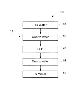
[0009] FIG. 1A is a cross-sectional diagram of a bonded quartz wafer
package
including silicon (Si) handling wafers, and FIG. 1B is a cross-sectional
diagram of the
bonded quartz wafer package of FIG. 1A after the Si handling wafers have been
removed,
in accordance with embodiments of the present disclosure;
[0010] FIG. 2 is a flow diagram of a general method suitable for packaging
the
bonded quartz wafer package of FIGS. 1A and 1B, in accordance with embodiments
of
the present disclosure;
[0011] FIG. 3 is a flow diagram of a method suitable for preparing a liquid
crystal
polymer (LCP) bonding layer and a first and second quartz wafer for bonding,
in
accordance with embodiments of the present disclosure;
[0012] FIG. 4 is a flow diagram of a method suitable for aligning a LCP
bonding layer
with a first quartz wafer, in accordance with embodiments of the present
disclosure;
[0013] FIG. 5 is a flow diagram of a method suitable for aligning a first
quartz wafer
with a second quartz wafer, in accordance with embodiments of the present
disclosure;
[0014] FIG. 6 is a flow diagram of a general method suitable for bonding to
form the
bonded quartz wafer package of FIGS. 1A and 1B, in accordance with embodiments
of
the present disclosure;
[0015] FIG. 7A and 7B is a flow diagram of an example method suitable for
bonding
to form the bonded quartz wafer package of FIGS. 1A and 1B using a wafer
bonder tool
3
CA 02939742 2016-08-18
280552-3
including an anodic pin top plate, in accordance with embodiments of the
present
disclosure;
[0016] FIG. 8A and 8B is a flow diagram of an example method suitable for
bonding
to form the bonded quartz wafer package of FIGS. 1A and 1B using a wafer
bonder
including a flat top plate, in accordance with embodiments of the present
disclosure;
[0017] FIG. 9 is a flow diagram of an example method suitable for dicing
the bonded
quartz wafer package of FIGS. 1A and 1B, in accordance with embodiments of the
present disclosure;
[0018] FIG. 10 is a top-down view of the quartz wafer package of FIG. 1A
that
includes numerous SAW devices, in accordance with embodiments of the present
disclosure;
[0019] FIG. 11 is a perspective view of a dice bonded quartz wafer package,
in
accordance with embodiments of the present disclosure;
[0020] FIG. 12 is a diagram of the quartz SAW device operating as a torque
sensor
disposed on a shaft, in accordance with embodiments of the present disclosure;
[0021] FIG. 13 is a model of forces impacting the quartz SAW device and
shaft of
FIG. 12, in accordance with embodiments of the present disclosure; and
[0022] FIG. 14 is a graph displaying viscoelastic properties of the LCP
oppositely
matching the viscoelastic properties of a die attached adhesive, in accordance
with
embodiments of the present disclosure.
DETAILED DESCRIPTION
[0023] One or more specific embodiments will be described below. In an
effort to
provide a concise description of these embodiments, all features of an actual
implementation may not be described in the specification. It should be
appreciated that in
4
CA 02939742 2016-08-18
280552-3
the development of any such actual implementation, as in any engineering or
design
project, numerous implementation-specific decisions must be made to achieve
the
developers' specific goals, such as compliance with system-related and
business-related
constraints, which may vary from one implementation to another. Moreover, it
should be
appreciated that such a development effort might be complex and time
consuming, but
would nevertheless be a routine undertaking of design, fabrication, and
manufacture for
those of ordinary skill having the benefit of this disclosure.
[0024] When introducing elements of various embodiments of the present
disclosure,
the articles "a," "an," "the," and "said" are intended to mean that there are
one or more of
the elements. The terms "comprising," "including," and "having" are intended
to be
inclusive and mean that there may be additional elements other than the listed
elements.
Furthermore, any numerical examples in the following discussion are intended
to be non-
limiting, and thus additional numerical values, ranges, and percentages are
within the
scope of the disclosed embodiments.
[0025] Single crystal quartz may provide certain benefits (e.g., precise
measurement
of frequencies of mechanical stresses) when functioning as piezoelectric
materials in
electrical devices. For example, the single crystal quartz may include surface
acoustic
wave (SAW) devices that use one or more interdigitating structures to convert
acoustic
waves into electrical signals by channeling the piezoelectric effect of the
single crystal
quartz. However, as noted above, some properties of single crystal quartz
provide
bonding challenges. One such challenge is that the coefficient of thermal
expansion
(CTE) of single crystal quartz can be lower than that of certain bonding
materials (e.g.,
glass frit materials). Further, another challenge is that single crystal
quartz is typically
fragile and can be easily broken when uneven stress is applied.
[0026] Accordingly, some embodiments of the present disclosure relate to
methods of
bonding single crystal quartz wafers that overcome the challenges. For
example, a
bonding layer with a CTE that closely matches the CTE for the single crystal
quartz may
be used. In some embodiments, the bonding layer may include a liquid crystal
polymer
CA 02939742 2016-08-18
280552-3
(LCP) material, which may provide both mechanical strength and hermetic
sealing. The
LCP bonding layer may be inserted in between two single crystal quartz wafers
(e.g., a
device wafer and a cap wafer) to facilitate effective bonding of the wafers
into a hermetic
wafer package. Further, bonding the two single crystal quartz wafers using the
LCP, as
presently disclosed, enables wafer bonding without the use of spacers or stand-
offs to
define a wafer-to-wafer gap. In addition, to overcome the delicateness of the
single
crystal quartz, handling wafers (e.g., Si handling wafers) may be placed above
and below
the single crystal quartz wafers to improve ease of handling and durability.
As discussed
in detail below, bonding forces, temperatures, and durations of forces may be
controlled
via a wafer bonder tool during the bonding process to enable effective bonding
of the
quartz wafer package. It may be appreciated that, while the remainder of the
disclosure
focuses on quartz-based SAW devices in particular, the presently disclosed
bonding
technique is applicable to the bonding of any quartz-based device.
[0027] FIGS. 1A
and 1B are cross-sectional diagrams of a bonded quartz wafer
package 10, in accordance with embodiments of the present disclosure. The
bonded
quartz wafer package 10 of FIG. 1A includes a stack 11 of materials that is
bonded
together, as described in detail below. The stack 11 is arranged prior to
bonding and
includes a first Si handling wafer 12, a first single crystal quartz wafer or
layer 14
disposed above the first Si handling wafer 12, a second single crystal quartz
wafer 16
disposed above the first single crystal quartz wafer 16, and a second Si
handling wafer 18
disposed above the second single crystal quartz wafer 18. As discussed in
greater detail
below, a LCP bonding layer 20 is disposed between the first quartz wafer 14
and the
second quartz wafer 16 in the stack 11. Further, the quartz wafer 14 may
include any
number of quartz-based devices (e.g., quartz SAW devices), and as such, the
first quartz
wafer 14 may be referred to herein as the device wafer 14. The second quartz
wafer 16
does not include any device structures, and as such, may be referred to herein
as the
capping wafer 16, because it provides the cap or ceiling for the cavities
around the
quartz-based devices of the device wafer 14. FIG. 1B illustrates the structure
of the
6
CA 02939742 2016-08-18
280552-3
bonded quartz wafer package 10 after the Si handling wafers 12 and 18 have
been
removed, as discussed below.
[0028] The thicknesses of the wafers 12, 14, 16, and 18 and the LCP bonding
layer 20
may be different in certain embodiments. In some embodiments, the first and
second Si
handling wafers 12 and 18 may have a thickness in a range of 100 micrometers
(gm)
thick to 2000 gm thick, the device wafer 14 and the capping wafer 16 may have
a
thickness in a range of 50 gm thick to 1000 gm thick, and the LCP bonding
layer 20 may
have a thickness in a range of 10 gm thick to 200 gm thick. In one example
embodiment,
the first and second Si handling wafers 12 and 18 may each be approximately
500
micrometers (gm) thick, the device wafer 14 and the capping wafer 16 may be
approximately 200 gm thick, and the LCP bonding layer 20 may be approximately
50 gm
thick. The LCP bonding layer 20 may be cut from a film having a predetermined
thickness to define the final cavity height (e.g., gap between the device
wafer 14 and the
capping wafer 16). Also, the LCP bonding layer 20 may have a lower CTE than
other
bonding materials (e.g., glass frit) and, thus, may better conform to the
single crystal
quartz material properties during bonding.
[0029] Another benefit of the LCP bonding layer 20 relates to its elastic
modulus. A
load may be shared between the device wafer 14 and the materials disposed
above the
device wafer 14 (e.g., LCP bonding layer 20). Thus, for quartz-based SAW
torque
sensors, for example, a stiffer bonding layer 20 results in a deceptively
lower strain
measurement by the SAW devices, since the strain is partially transferred to
the stiffer
bonding layer 20. Accordingly, the presently disclosed LCP bonding layer 20
has a
lower elastic modulus than some other bonding materials (e.g., glass frit)
and, therefore, a
greater amount of the strain is able to reach and be detected by the SAW
devices of the
device wafer 14. As a result, the LCP bonding layer 20 enables greater
sensitivity and
enhanced accuracy for certain types of quartz-based devices (e.g., quartz SAW
devices)
compared to other types of bonding materials.
7
CA 02939742 2016-08-18
280552-3
[0030] As previously noted, the Si handling wafers 12 and 18 may be used to
inhibit
the fragile single crystal quartz from cracking during bonding by adding
thickness and
mechanical strength to the stack 11. However, after the stack 11 is bonded,
the first and
second Si handling wafers 12 and 18 may be removed, resulting in the bonded
quartz
wafer package 10 depicted in FIG. 1B. It should be noted that the bonded
quartz wafer
package 10 shown in FIG. 1B may be diced into individual dice bonded quartz
wafer
packages 21 and a die attached adhesive layer 22 may be applied to each dice
bonded
quartz wafer package 21. The die attached adhesive layer 22 may be used to
attach the
dice bonded quartz wafer package 21 to a component to be monitored, such as a
shaft of a
helicopter, airplane, automobile, boat, transmission, and the like. It should
be noted that
the die attached adhesive layer 22 may couple to any suitable substrate. As
will be
discussed in detail below, in certain embodiments, the viscoelastic properties
of the die
attached adhesive layer 22 and the LCP bonding layer 20 may be matched to
provide a
self-compensating dice bonded quartz wafer package 21. As shown, the die
attached
adhesive layer 22 is exposed and may be used to couple a portion of the dice
bonded
quartz wafer package 21 to a suitable structure.
[0031] It should be understood that, in some embodiments, the quartz-based
devices
present within the device wafer 14 may function as SAW torque sensors. For
example, as
mentioned above, after dicing, the packaged SAW torque sensors may be placed
on any
suitable part of an aircraft, automobile, or machine, such as a shaft. When
torque is
applied to the shaft, there is an external strain on the shaft that is
transferred to the device
wafer 14 of the dice bonded quartz wafer package 21, through the die attached
adhesive
22. A surface acoustic wave indicative of the strain propagates across the
single crystal
quartz material, and the frequency of the wave may increase and decrease
between
interdigitating structures of the SAW devices of the device wafer 14 based on
the spacing
of the interdigitating structures. That is, as the single crystal quartz
material is strained,
the spacing of the interdigitating structures may change and the frequency may
change.
A processor that receives electrical signals indicative of the wave from the
torque sensor
8
CA 02939742 2016-08-18
280552-3
may be analyzed by a processor to determine the frequency of the wave (e.g.,
strain) and
the orientation of the interdigitating structures.
[0032] FIG. 2 is a flow diagram of a general method 30 suitable for
packaging the
bonded quartz wafer package 10 of FIGS. 1A and 1B, in accordance embodiments
of the
present disclosure. It should be noted that the details of each step of the
method 30 are
described in further detail in separate flow diagrams below. In other
embodiments, the
method 30 may include fewer steps and/or steps performed in orders different
than the
embodiment presented in FIG. 2.
[0033] The embodiment of the method 30 illustrated in FIG. 2 includes
preparing the
LCP bonding layer 20, device wafer 14, and capping wafer 16 for bonding
(method block
32). The illustrated method 30 also includes aligning the LCP bonding layer 20
with the
device wafer 14 in the stack 11 (method block 34) and aligning the device
wafer 14 with
the capping wafer 16 in the stack 11(method block 30). The illustrated method
30 also
includes bonding the stack 11 to form the bonded quartz wafer package 10
(method block
38) and dicing the bonded quartz wafer package 10 into individual dice bonded
quartz
wafer packages 21 (method block 40).
[0034] More specifically, FIG. 3 is a flow diagram of an embodiment of a
method 42
suitable for preparing the LCP bonding layer 20, the device wafer 14, and the
capping
wafer 16 for bonding (method block 32 of FIG. 2). The method 42 illustrated in
FIG. 3
includes obtaining a LCP sheet material for the LCP bonding layer 20 (method
block 44)
and cutting (e.g., laser cutting) openings in the sheet material (method block
46) to fit
around the devices of the device wafer 14 when the LCP sheet material is
disposed
between the device wafer 14 and capping wafer 16. Additionally, the method 42
illustrated in FIG. 3 includes vacuum baking the LCP sheet material for a
desired time
period (e.g., 1, 2, 3, 4, or 5 hours) at a desired temperature (e.g., 100,
105, 110, 115, or
120 C) (method block 48). The method 42 illustrated in FIG. 3 also includes
plasma
ashing the wafers 14 and 16 for a desired time period (e.g., 1, 2, 3, 4, 5, or
6 minutes) in
any suitable structure (e.g., barrel) (method block 50).
9
CA 02939742 2016-08-18
280552-3
[0035] FIG. 4 is a flow diagram of an embodiment of a method 52 suitable
for
aligning the LCP bonding layer 20 with the device wafer 14 (method block 34 of
FIG. 2),
in accordance with embodiments of the present disclosure. The method 52
illustrated in
FIG. 4 includes placing the device wafer 14 onto the first Si handle wafer 12
(method
block 54). In some embodiments, a 500 lam thick Si handle wafer may be used
for the
first Si handle wafer 12. However, any desired thickness may be used, as
appropriate
(e.g., 400, 450, 500, 550, or 600 ,m). The illustrated method 52 includes
overlaying the
baked LCP bonding layer 20 onto the device wafer 14 (method block 56). Then,
the
illustrated method 52 includes aligning fiducial markers of the LCP bonding
layer 20
with fiducial markers of the device wafer 14 (method block 58). In certain
embodiments,
the alignment of method block 58 may be performed manually using a zoom scope
or
automatically using an alignment device. The illustrated method 52 may also
include
using a cover piece of glass to hold the LCP bonding layer 20 in place on the
device
wafer 14 (method block 60). The LCP bonding layer 20 may be tacked to the
device
wafer 14 around the perimeter of the LCP bonding layer 20 a desired distance
apart (e.g.,
1-5 millimeters (mm), 5-10 mm, or 10-15 mm) (method block 62). In some
embodiments, a soldering iron may be used to tack the LCP bonding layer 20 to
the
device wafer 14 and the soldering iron may be set to a desired temperature
(e.g., 640,
650, 660, 670, or 680 F). The illustrated method 52 also includes removing
the cover
glass (method block 64).
[0036] FIG. 5 is a flow diagram of an embodiment of a method 66 suitable
for
aligning a first quartz wafer with a second quartz wafer (method block 36 of
FIG. 2). The
illustrated method 66 includes placing the first Si handle wafer 12 and device
wafer 14,
with the attached LCP bonding layer 20, onto a wafer bonder transport fixture
(method
block 68). The loading of method block 68 may include verifying that the first
Si handle
wafer 12 and the device wafer 14 have a flat orientation in the wafer bonder
transport
fixture. In some embodiments, as a result of using the LCP bonding layer 20,
the bonded
quartz wafer package 10 may not include spacers disposed between the device
wafer 14
and the capping wafer 16. However, it should be noted that, in some
embodiments, the
CA 02939742 2016-08-18
280552-3
illustrated method 66 may include placing spacers (e.g., 40 micron) into
cavity locations
(e.g., 8, 9, or 10 locations) on the device wafer 14 (optional method block
70).
[0037] Further, the illustrated method 66 also includes aligning flats of
the capping
wafer 16 and the second Si handling wafer 18 together (method block 72). The
second Si
handling wafer may be 500 gm thick. However, any appropriate thickness (e.g.,
400,
450, 500, 550, or 600 gm) may be used for the second Si handling wafer 18.
Then, the
capping wafer 16 and the second Si handling wafer 18 may be placed on top of
the device
wafer 14 in the wafer bonder transport fixture to form the stack 11 (method
block 74).
The illustrated method 66 also includes applying clamps of the wafer bonder
transport
fixture to hold the stack 11 in place (method block 76).
[0038] Once the stack 11 is arranged in the wafer bonder transport fixture,
the wafer
bonder transport fixture may be loaded onto a bonder tool and a set of
instructions
representing a bonding process (e.g., a "recipe") may be loaded on the wafer
bonder tool.
The instructions may be executed by the wafer bonder tool to run the bonding
process.
FIGS. 6-8 illustrate flow diagrams of example embodiments of methods including
instructions for bonding the device wafer 14 and the capping wafer 16 via the
LCP
bonding layer 20 to form the bonded quartz wafer package 10.
[0039] Starting with FIG. 6, a flow diagram of an embodiment of a general
method 80
suitable for bonding the stack 11 to form the bonded quartz wafer package of
FIGS. IA
and 1B (method block 38 of FIG. 2) is illustrated. The illustrated method 80
includes
loading the wafer bonder transport fixture including the quartz wafer package
(e.g., stack
11) into the wafer bonder tool (method block 82) and applying a contact pin of
the wafer
bonder tool (method block 84). The contact pin of the wafer bonder tool may
provide
clamping force to keep the components of the stack 11 from moving and losing
alignment. Next, the method 80 may include pump purging the sealed chamber of
the
wafer bonder tool that contains the stack 11 with nitrogen or other desired
atmosphere
(method block 86). Pump purging the sealed chamber may enable controlling the
11
CA 02939742 2016-08-18
280552-3
environment in the chamber and also the device cavities from undesirable
elements (e.g.,
moisture).
[0040] The illustrated method 80 also includes ramping (e.g., increasing)
to a first
temperature (e.g., 250, 275, 300, 325, or 350 C) inside the chamber over a
desired time
period (e.g., 800, 850, 900, or 950 seconds). The first temperature may enable
thermal
expansion of the LCP and/or the quartz material to facilitate bonding. Then,
once the
first temperature is reached, a first force (e.g., 1, 2, 3, or 4 psi) may be
applied by the
contact pin (method block 90). In some instances, the force of the contact pin
may
minimize bowing of the quartz materials in the device wafer 14 and capping
wafer 16.
After the first force is applied, the illustrated method 80 includes dwelling
at the first
temperature and the first force for a desired time period (e.g., 13, 14, 15,
16, 17 minutes)
(method block 92) to allow the quartz layers 14 and 16, the LCP bonding layer
20, and
the Si handle wafers 12 and 18 to equilibrate.
[0041] Continuing through the method 80 illustrated in FIG. 6, after the
desired time
period expires, the illustrated method 80 includes cooling to a second
temperature (e.g.,
200, 225, 250, 275, or 300 C), lower than the first temperature, over a
desired period of
time (e.g., 13, 14, 15, 16, 17 minutes) (method block 94). Slowly cooling to
the second
temperature may enable movement of the quartz layers 14 and 16 and LCP bonding
material 20 while equilibrating and inhibit cracking of the single crystal
quartz materials.
Then, the force from the contact pin may be removed (method block 96) and the
chamber
may be cooled to a third temperature (e.g., 30, 35, 40, or 45 C), lower than
the first and
second temperatures, over a desired time period. (e.g., 500, 550, 600, or 650
seconds).
Then, the bonding process concludes and the wafer bonder transport fixture is
unloaded
from the bonder tool (method block 100). At the end of the illustrated method
80, the
device wafer 14 and the capping wafer 16 are bonded via the LCP bonding layer
20 to
form the bonded quartz wafer package 10.
[0042] FIG. 7A and 7B is a flow diagram of an embodiment of a method 110
suitable
for bonding the stack 11 to form the bonded quartz wafer package 10 of FIGS.
1A and 1B
12
CA 02939742 2016-08-18
280552-3
(method block 38 of FIG. 2) using a wafer bonder tool including an anodic pin
top plate.
The illustrated method 110 includes loading the wafer bonder transport fixture
including
the quartz wafer package (e.g., stack 11) into the wafer bonding tool (method
block 112).
The chamber of the bonder tool may be purged with nitrogen to prevent moisture
from
affecting the environment inside the cavities of the devices (e.g., SAW
devices) of the
device wafer 14 (method block 114). Then, the top pin may be applied to make
contact
with the stack 11 (method block 116) and the wafer bonder transport fixture
clamps may
be removed (method block 118), since the top pin is holding the materials of
the stack 11
in place. The method 110 may include pump purging the chamber a desired number
of
times (e.g., 1, 2, 3, 4, 5) (method block 120) to further control the
environment in and
around the stack 11.
[0043] The illustrated method 110 includes ramping to a first temperature
(e.g., 135,
140, 145, 150, 155 C) inside the chamber over a desired time period (e.g.,
800, 850, 900,
950 seconds) (method block 122). Then, once the first temperature is reached,
the
illustrated method 110 includes dwelling at the first temperature for a
desired time period
(e.g., 13, 14, 15, 16, 17 minutes) (method block 124) to allow the quartz
materials, LCP,
and Si to equilibrate. After the desired time period expires, the method 110
may include
ramping to a second temperature (e.g., 280, 290, 300, 310, 320 C), higher
than the first
temperature, over a desired period of time (e.g., 1600, 1700, 1800, 1900, 2000
seconds)
(method block 126). Once the second temperature is reached, the illustrated
method 110
includes dwelling at the second temperature for a desired time period (e.g.,
25, 30, 35, 40,
45 minutes) (method block 128). The wafer bonder tool may apply force (e.g.,
135, 150,
165 millibar) via the anodic top pin (method block 130) so the LCP bonding
layer 20, the
device wafer 14, and capping wafer 16 are pressed together to facilitate
bonding.
[0044] The illustrated method 110 includes cooling to a third temperature
(e.g., 240,
250, 260 C) over a desired time period. (e.g., 500, 550, 600, 650 seconds)
(method block
132). Then, the wafer bonder tool force may be removed (method block 134) and
the
temperature may be cooled to a fourth temperature (e.g., 90, 100, 110 C) over
a desired
13
CA 02939742 2016-08-18
280552-3
time period (e.g., 1100, 1200, 1300 seconds) (method block 136). Once at the
fourth
temperature, the temperature may be cooled again to a fifth temperature (e.g.,
30, 40, 50
C) over a desired time period (e.g., 550, 600, 650 seconds) (method block
138). The
bonding process may subsequently conclude and the wafer bonder transport
fixture may
be unloaded from the bonder tool (method block 140). At the end of the
illustrated
method 80, the device wafer 14 and the capping wafer 16 are bonded via the LCP
bonding layer 20 to form the bonded quartz wafer package 10 illustrated in
FIGS. 1A and
1B.
[0045] FIG. 8A and 8B is a flow diagram of an embodiment of a method 150
suitable
for bonding the stack 11 to form the bonded quartz wafer package 10 (e.g.,
stack 11) of
FIGS. 1A and 1B (method block 38 of FIG. 2) using a wafer bonder tool
including a flat
top plate. The flat top plate has a larger surface area than the anodic pin
top plate and,
thus, the differences between the method 150 of FIG. 8 and the method 110 of
FIG. 7
may include when to apply pressure/force using the larger plate. The
illustrated method
150 includes loading the wafer bonder transport fixture including the quartz
wafer
package (e.g., stack 11) into the bonder tool (method block 152). The chamber
of the
bonder tool may be purged with nitrogen to prevent moisture from affecting the
environment inside the device cavities of the device wafer 14 (method block
154). The
method 150 may also include pump purging the chamber a desired number of times
(e.g.,
1, 2, 3, 4, 5) (method block 120) to further control the environment in and
around and
inside the stack 11.
[0046] Then, the illustrated method 150 includes ramping to a first
temperature (e.g.,
135, 140, 145, 150, 155 C) inside the chamber over a desired time period
(e.g., 800, 850,
900, 950 seconds) (method block 158). Once the first temperature is reached,
the method
150 includes dwelling at the first temperature for a desired time period
(e.g., 13, 14, 15,
16, 17 minutes) (method block 160) to allow the quartz materials, LCP, and Si
to
equilibrate. After the desired time period expires, the method 150 may include
ramping
to a second temperature (e.g., 280, 290, 300, 310, 320 C), higher than the
first
14
CA 02939742 2016-08-18
280552-3
temperature, over a desired period of time (e.g., 1600, 1700, 1800, 1900, 2000
seconds)
(method block 162). Once the second temperature is reached, the method 150
includes
dwelling at the second temperature for a desired time period (e.g., 33, 34,
35, 36, or 37
minutes) (method block 164). Then, the top plate may be applied to make
contact with
the stack 11 (method block 166) and the wafer bonder transport fixture clamps
may be
removed (method block 168), since the top plate is holding the materials of
the stack 11
in place. Force (e.g., 140, 145, 150, 155, or 160 mBar) may be applied by the
wafer
bonding tool (method block 170).
[0047] The illustrated method 110 also includes cooling the chamber to a
third
temperature (e.g., 240, 250, 260 C) over a desired time period. (e.g., 500,
550, 600, 650
seconds) (method block 172). Then, the wafer bonder tool force may be removed
(method block 174) and the chamber may be cooled to a fourth temperature
(e.g., 90,
100, 110 C) over a desired time period (e.g., 1100, 1200, 1300 seconds)
(method block
176). Once at the fourth temperature, the chamber may be cooled again to a
fifth
temperature (e.g., 30, 40, 50 C) over a desired time period (e.g., 550, 600,
650 seconds)
(method block 178). The bonding process may subsequently conclude and the
wafer
bonder transport fixture may be unloaded from the bonder tool (method block
180). At
the end of the method 150, the device wafer 14 and the capping wafer 16 are
bonded via
the LCP bonding layer 20 to form the bonded quartz wafer package 10.
[0048] In some embodiments, the quartz layers 14 or 16 of the bonded quartz
wafer
package 10 may be thinned post-bonding. For SAW torque sensors, for example,
thinning the bonded quartz wafer package 10 may increase the strain
sensitivity of the
SAW devices of the device layer 14 by reducing the amount of materials that
can absorb
transferred strain.
[0049] Once the stack 11 has been successfully bonded, the bonded quartz
wafer
package 10 may be diced into individual device dies (e.g., dice bonded quartz
wafer
packages 21). Accordingly, FIG. 9 is a flow diagram of an embodiment of a
method 190
suitable for dicing the bonded quartz wafer package 10 of FIGS. 1A and 1B
(method
CA 02939742 2016-08-18
280552-3
block 40 of FIG. 2), in accordance with embodiments of the present disclosure.
The
illustrated method 190 includes performing a bevel cut at a particular angle
(e.g., 45 ) to
reveal wire pad areas that protrude underneath a seal ring (method block 192).
The bevel
cut performed of method block 192 may only dice through the capping wafer 16.
Then,
another bevel cut may be performed at a particular angle (e.g., 45 ) along
four sides
surrounding individual devices that partially cuts into the device wafer 14
(method block
194). Last, a straight cut is performed on each of four sides of the
individual devices of
the bonded quartz wafer package 10 that cuts all the way through the bonded
quartz wafer
package 10 (method block 196). After the method block 196, each of the devices
of the
bonded quartz wafer package 10 may be a dice bonded quartz wafer package 21.
The
illustrated method 190 allows the dicing of the bonded quartz wafer package 10
in a
manner that minimizes the amount of the device wafer 14 that is exposed. In
addition, a
barrier coating (e.g., silicon nitride, aluminum oxide, silicon oxide, metal,
titanium) may
be applied over the dice bonded quartz wafer packages 10 for additional
hermeticity.
[0050] FIG. 10 is a top-down image of a bonded quartz wafer package 10
including
numerous SAW devices 200 disposed thereon, in accordance with embodiments of
the
present disclosure. As should be appreciated, since the depicted embodiment of
the
bonded quartz wafer package 10 does not include spacers, more SAW devices 200
are
able to fit onto the bonded quartz wafer package 10 than if spacers were used.
As
illustrated in the blown up perspective view 201, the SAW device 200 includes
a cavity
202 formed between the device wafer 14 and the capping wafer 16. Three
interdigitating
structures 204 are disposed inside the cavity 202 and are capable of
converting surface
acoustic waves to electrical signals. Also, each SAW device 200 includes an
interconnect
206 disposed within the cavity 202. In addition, each SAW device 200 may
include a
wire pad 208 that enables electrical coupling to the device 200.
[0051] FIG. 11 is a perspective view of a dice bonded quartz wafer package
21, in
accordance with embodiments of the present disclosure. The dice bonded quartz
wafer
package 21 results from singulation of the bonded quartz wafer package 10
(e.g., dicing
16
CA 02939742 2016-08-18
280552-3
the bonded quartz wafer package 10 into individual device dies), as described
above. As
illustrated, the dice bonded quartz wafer package 21 includes the device wafer
14 and the
capping wafer 16 bonded via the LCP bonding layer 20. Also, the SAW device 200
includes the interdigitating structures 204 disposed in the cavity 202 formed
between the
device wafer 14 and the capping wafer 16. Further, as depicted, the wire pad
208 (e.g.,
I/O pads) is exposed to enable electrical coupling to the SAW device 200 of
the dice
bonded quartz wafer package 21.
[0052] FIG. 12 is a diagram of a dice bonded quartz wafer package 21 (i.e.,
a die of
the bonded quartz wafer package 10 after dicing) operating as a torque sensor
209
disposed on a shaft 210, in accordance with embodiments of the present
disclosure. FIG.
13 is a model 212 of forces impacting the torque sensor 209 and the shaft 210
of FIG. 12,
in accordance with embodiments of the present disclosure. FIG. 14 is a graph
214
displaying viscoelastic properties of the LCP bonding layer 20 oppositely
matching and
counteracting the viscoelastic properties of the die attached adhesive 22. For
clarity, the
figures are discussed together below. It should be noted that FIGS. 12 and 13
include
abbreviations for a spring, denoted by "S," and for a spring damper, denoted
by "SD."
[0053] As depicted in FIG. 12, the torque sensor 209 may be attached to the
shaft 210
(e.g., steel) via the die attached adhesive 22. As previously discussed, when
torque is
applied to the shaft 210, there is a stress or strain on the shaft 210 that
may transfer
through the die attached adhesive 22 to the single crystal quartz of the
device wafer 14
that includes the SAW device(s), the LCP bonding layer 20, and the single
crystal quartz
of the capping wafer 16. Thus, the shaft 210 may function as a spring that
supplies a
stress or strain to the torque sensor 209. The die attached adhesive 22 may
function as a
spring damper, the device wafer 14 may function as a spring, the LCP bonding
layer 20
may function as a spring damper, and the capping wafer 16 may function as a
spring.
[0054] The force model 212 of FIG. 13 helps illustrate the time dependence
of
viscoelastic properties of the adhesives of the torque sensor 209. There are
two adhesives
of the torque sensor 209: the die attached adhesive 22 and the LCP bonding
layer 20. As
17
CA 02939742 2016-08-18
280552-3
depicted, a delta X strain may be applied by the steel shaft. At time 0, a
load is carried to
the die attached adhesive 22 due to overall displacement. The strain in the
spring at the
top of the device wafer 14 is the SAW output 216 that may be processed by a
processor
to determine the frequency of the strain. As the strain is transferred through
the die
attached adhesive 22, the spring damper comes into effect, and the spring
constant of the
die attached adhesive 22 becomes less on both sides of the adhesive 22,
thereby
decreasing the strain over time. That is, the viscoelastic properties of the
die attached
adhesive 22 causes the strain to decrease over time, which may affect the
measurement of
the strain by the torque sensor 209. However, the viscoelastic properties of
the LCP
bonding layer 20 provide an opposite, balancing effect, increasing strain over
time to
cancel out the aforementioned decreased strain of the die attached adhesive
22. Using
LCP as the bonding layer provides the benefit of enabling matching of the
viscoelastic
time dependent behavior of the LCP bonding layer 20 and the die attached
adhesive 22.
In combination, the die attached adhesive 22 and the LCP bonding layer 22 can
provide a
self-compensating structure.
[0055] The die attached adhesive effect 218 and the LCP effect 220 are also
depicted
in the graph 214 of FIG. 14. As depicted, the die attached adhesive effect 218
shows the
strain decreasing over time, while the LCP effect 220 shows the strain
increasing over
time. As such, for the torque sensor 209, the two effects can counteract one
another to
enable accurate torque measurements to be obtained.
[0056] Technical effects of the techniques include providing a quartz-based
device
that is bonded together via a LCP bonding layer. The bonding methods disclosed
herein
can overcome the challenges typically associated with single crystal quartz,
such as its
fragileness and its low coefficient of thermal expansion (CTE). As described
above, the
LCP bonding material provides several advantages, such as having a similar CTE
to the
single crystal quartz, a low elastic modulus to enhance sensitivity of the SAW
devices,
and time dependent viscoelastic properties that oppositely match the
viscoelastic
18
CA 02939742 2016-08-18
280552-3
properties of the die attached adhesive 22, thereby enabling more accurate
strain
measurements by the SAW devices.
[0057] While there
have been described herein what are considered to be preferred
and exemplary embodiments of the present invention, other modifications of
these
embodiments falling within the scope of the invention described herein shall
be apparent
to those skilled in the art.
19