Note: Descriptions are shown in the official language in which they were submitted.
X-RAY COLLIMATOR
The present invention relates generally to an x-ray collimator and a method of
obtaining an x-ray image and finds particular, although not exclusive, utility
in the
collimation of x-ray Bremsstrahlung radiation, where the x-ray source
comprises a
plurality of x-ray sources arranged in a two dimensional array.
BACKGROUND OF THE INVENTION
It is known that collimation of x-rays results in an improvement in the image
quality of an x-ray imaging system. This is because the collimation of an x-
ray source
reduces the amount of scattered x-ray photons which reach the x-ray sensor
elements,
after having passed through the subject matter being imaged. These scattered x-
ray
photons would otherwise contribute to the reading from the sensor elements and
reduce
the overall contrast in the x-ray image because thcy do not convey the same
relevant
diagnostic information as the unscattered x-ray photons that have passed
directly from
the x-ray source to the sensor element. Scattered photons are responsible for
the haze
often associated with radiographs.
Generally, prior art x-ray collimators have comprised a two dimensional grid,
sometimes also known as an anti-scatter grid (ASG), which is positioned
directly in front
of the sensor and serves to absorb or block photons emanating with a large
angle. These
ASGs are often grid structures composed of high density metals whose operation
can be
considered analogous to a venetian blind collimating optical photons. A
variety of
geometries and fabrication methods have been described in the literature, each
with the
similar goal of reducing the unwanted scattered photons from impinging upon
the sensor.
In addition to anti-scatter methods, x-ray lenses have been considered. A wide
range of approaches has been discussed in an attempt to focus x-rays with more
efficiency
or better focal properties. Examples of prior art x-ray lenses include,
polycapillaries
(assembled and fused) and Wolter Optics (a grid of materials) both of which
essentially
work by collectively reflecting a single source of x-ray photons. Refractive
lenses have
also been described.
In recent years there have been advances in the development of micrometer
scale
x-ray sources, such that it is now possible to produce a two dimensional array
of x-ray
sources with a typical distance between the x-ray sources of the order of 100
[trn to 1cm
or more.
1
Date Recue/Date Received 2021-07-07
An example of such a two-dimensional x-ray source is provided in WO
2011/017645 apparatus for producing x-rays for use in imaging.
Known collimation and lensing methods are not so useful for collimating a two
dimensional array of x-ray sources and it is an aim of embodiments of the
present
invention to at least partially mitigate the disadvantages of known x-ray
collimation
methods and to provide a means of collimating x-rays emanating from a two-
dimensional
array of x-ray sources.
SUMMARY OF THE INVENTION
It is an aim of the present invention to provide a means of collimating x-rays
whereby multiple collimating elements or holes receive x-ray photons from a
single x-ray
source. It is a further aim of the present invention to provide a means of
collimating x-
rays whereby each collimating element or hole comprises a tapered geometry of
high
aspect ratio and is aligned with a micrometer scale two-dimensional array of x-
ray sources,
so that the x-ray output angle and distribution is controlled on an emitter by
emitter basis
in a distributed x-ray source. In this regard, a high aspect ratio may include
one which
has a height to width ratio of the order of 10:1 to 1000:1.
In a first aspect the invention provides an x-ray collimator comprising a
substrate
containing a plurality of collimator holes, wherein at least some of said
collimator holes
comprise along their axial lengths, an entrance hole through which x-rays may
pass into
the collimator holes, a frustoconical tapered portion, and a following tubular
portion
having an output hole, wherein the x-ray collimator further comprises x-ray
target material
comprising a first sheet of high atomic number material and being arranged to
convert,
in use, electrons from an array of electron emitters into localised sources of
x-ray photons,
such that each of said at least some collimator holes emits a beam of x-ray
photons
emerging from the output hole in a cone which is approximately parallel or has
an angle
of deviation from parallel in the range 1 to 20 degrees.
The plurality of holes may be arranged in a two dimensional array. The two-
dimensional array may be in the form of a grid. The gird may be regularly
arranged such
as in regularly spaced columns and rows. Alternatively, the grid may be
irregular.
The substrate may comprise silicon or a glass. The glass may be fused silica.
The frustoconical portion may be described by an approximate parabolic shape.
The parabolic shape may be defined approximately by a shape known as a
"Winston
Cone". The tubular portion may be cylindrical.
Date Recue/Date Received 2021-07-07
The distance between the entrance hole of the frustoconical portion and the
output hole of the tubular portion may be substantially greater than the
diameter of the
output hole, this geometry being configured in order to achieve a reduction in
the opening
angle of the transmitted x-rays compared to the opening angle of the unguided
radiation.
The distance between the entrance hole of the frustoconical portion and the
output hole of the tubular portion may be known as the "nominal collimator
length".
The nominal collimator length may be at least ten times greater than the
diameter
of the output hole, this geometry being configured in order to achieve a
reduction in the
opening angle of the transmitted x-rays compared to the opening angle of the
unguided
radiation.
The ratio of the nominal collimator length to the output diameter may be
described as the collimator's "aspect ratio".
The holes running through the substrate may be lined on their inner surface
with
a thin film. The thin film may comprise at least a single layer of either
tungsten or iridium.
The thin film may comprise a bi-layer of one of tungsten and aluminium oxide,
tungsten
and silicon, and tungsten and carbon. The thin film may comprise a bi-layer
combination
of a high Z number metal and a low Z number/low density spacer material. In
this regard
the term "low" may mean having a lower atomic number than the "high Z number
metal".
The "low Z number material" may have an atomic number only one less than the
"high
Z number metal". A bi-layer may be said to comprise a stack of thin films.
The x-ray collimator may further include a target material comprising a first
thin
sheet of a high atomic number material, the first thin sheet acting as a
target material
converting a source of electrons from an array of electron emitters into
localised sources
of x-ray photons, wherein the input of the frustoconical portion may be
abutted against
the target material.
The first thin sheet may comprise one or more of tungsten, tungsten alloy,
molybdenum or gold. The first thin sheet of the target material may have a
thickness of
approximately of 1 to 5 lam.
A second thin sheet of x-ray filter material may be positioned between the
target
material and the frustoconical hole openings in the substrate. The x-ray
filter material may
comprise aluminium.
The x-ray filter material may have a thickness of approximately 100 to 500
p.m.
3
Date Recue/Date Received 2021-07-07
In a third aspect, the invention provides a method of obtaining an x-ray image
of
a subject, comprising the steps of providing an x-ray collimator according to
the first
aspect, aligning said x-ray collimator with a two-dimensional x-ray sensor,
whereby, in
use, x-ray photons from the x-ray sources pass through the collimator holes
and emerge
in a narrow angle cone of x-ray photons some of which then pass through a
subject
positioned between the output holes of the collimator and the x-ray sensor.
In one embodiment, the invention provides a method of obtaining an x-ray image
of a subject, comprising the steps of providing an x-ray collimator in
accordance with the
first aspect providing an array of x-ray sources, providing an array of x-ray
sensing
elements and aligning the x-ray collimator input holes with the array of x-ray
sources and
aligning the x-ray collimator output holes with the array of x-ray sensing
elements,
whereby x-ray photons from the array of x-ray sources pass through the
collimator holes
and emerge as an approximately parallel beam of x-ray photons which pass
through a
subject positioned between the output holes of the collimator and the array of
x-ray
sensing elements. The array of x-ray sources may be two-dimensional. The array
of x-
ray sensing elements may be two-dimensional.
Embodiments of the invention have the advantage that they provide a means to
collimate x-rays emanating from a two-dimensional array of micrometer scale x-
ray
sources.
BRIEF DESCRIPTION OF THE DRAWINGS
The above and other characteristics, features and advantages of the present
invention will become apparent from the following detailed description, taken
in
conjunction with the accompanying drawings, which illustrate, by way of
example, the
principles of the invention. This description is given for the sake of example
only, without
limiting the scope of the invention. The reference figures quoted below refer
to the
attached drawings.
Figure 1 is a plan view of an x-ray collimator;
Figure 2 is a schematic cross-section of an x-ray collimator;
Figure 3 is a schematic cross-section of the x-ray collimator of Figure 2
coupled
to an x-ray target material and electron source;
Figure 4 is a schematic cross-section of the x-ray collimator of Figure 3
including
an x-ray filter material; and
4
Date Recue/Date Received 2021-07-07
Figure 5 is a schematic cross-section of two x-ray collimators of Figure 4 in
conjunction with a subject matter to be imaged onto adjacent elements in a two-
dimensional x-ray sensor.
DETAILED DESCRIPTION
The present invention will be described with respect to certain drawings but
the
invention is not limited thereto but only by the claims. The drawings
described are only
schematic and are non-limiting. Each drawing may not include all of the
features of the
invention and therefore should not necessarily be considered to be an
embodiment of the
invention. In the drawings, the size of some of the elements may be
exaggerated and not
drawn to scale for illustrative purposes. The dimensions and the relative
dimensions do
not correspond to actual reductions to practice of the invention.
Furthermore, the terms first, second, third and the like in the description
and in
the claims, are used for distinguishing between similar elements and not
necessarily for
describing a sequence, either temporally, spatially, in ranking or in any
other manner. It
is to be understood that the terms so used are interchangeable under
appropriate
circumstances and that operation is capable in other sequences than described
or
illustrated herein.
Moreover, the terms top, bottom, over, under and the like in the description
and
the claims are used for descriptive purposes and not necessarily for
describing relative
positions. It is to be understood that the terms so used are interchangeable
under
appropriate circumstances and that operation is capable in other orientations
than
described or illustrated herein.
It is to be noticed that the term "comprising", used in the claims, should not
be
interpreted as being restricted to the means listed thereafter; it does not
exclude other
elements or steps. It is thus to be interpreted as specifying the presence of
the stated
features, integers, steps or components as referred to, but does not preclude
the presence
or addition of one or more other features, integers, steps or components, or
groups
thereof. Thus, the scope of the expression "a device comprising means A and B"
should
not be limited to devices consisting only of components A and B. It means that
with
respect to the present invention, the only relevant components of the device
are A and B.
Similarly, it is to be noticed that the term "connected", used in the
description,
should not be interpreted as being restricted to direct connections only.
Thus, the scope
of the expression "a device A connected to a device B" should not be limited
to devices
5
Date Recue/Date Received 2021-07-07
or systems wherein an output of device A is directly connected to an input of
device B.
It means that there exists a path between an output of A and an input of B
which may be
a path including other devices or means. "Connected" may mean that two or more
elements are either in direct physical or electrical contact, or that two or
more elements
are not in direct contact with each other but yet still co-operate or interact
with each other.
For instance, wireless connectivity is contemplated.
Reference throughout this specification to "an embodiment" or "an aspect"
means that a particular feature, structure or characteristic described in
connection with
the embodiment or aspect is included in at least one embodiment or aspect of
the present
invention. Thus, appearances of the phrases "in one embodiment", "in an
embodiment",
or "in an aspect" in various places throughout this specification are not
necessarily all
referring to the same embodiment or aspect, but may refer to different
embodiments or
aspects. Furthermore, the particular features, structures or characteristics
of any
embodiment or aspect of the invention may be combined in any suitable manner,
as
would be apparent to one of ordinary skill in the art from this disclosure, in
one or more
embodiments or aspects.
Similarly, it should be appreciated that in the description various features
of the
invention are sometimes grouped together in a single embodiment, figure, or
description
thereof for the purpose of streamlining the disclosure and aiding in the
understanding of
one or more of the various inventive aspects. This method of disclosure,
however, is not
to be interpreted as reflecting an intention that the claimed invention
requires more
features than are expressly recited in each claim. Moreover, the description
of any
individual drawing or aspect should not necessarily be considered to be an
embodiment
of the invention. Rather, as the following claims reflect, inventive aspects
lie in fewer
than all features of a single foregoing disclosed embodiment.
Furthermore, while some embodiments described herein include some features
included in other embodiments, combinations of features of different
embodiments are
meant to be within the scope of the invention, and form yet further
embodiments, as will
be understood by those skilled in the art. For example, in the following
claims, any of the
claimed embodiments can be used in any combination.
In the description provided herein, numerous specific details are set forth.
However, it is understood that embodiments of the invention may be practised
without
these specific details. In other instances, well-known methods, structures and
techniques
6
Date Recue/Date Received 2021-07-07
have not been shown in detail in order not to obscure an understanding of this
description.
In the discussion of the invention, unless stated to the contrary, the
disclosure of
alternative values for the upper or lower limit of the permitted range of a
parameter,
coupled with an indication that one of said values is more highly preferred
than the other,
is to be construed as an implied statement that each intermediate value of
said parameter,
lying between the more preferred and the less preferred of said alternatives,
is itself
preferred to said less preferred value and also to each value lying between
said less
preferred value and said intermediate value.
The use of the term "at least one" may mean only one in certain circumstances.
The principles of the invention will now be described by a detailed
description of
at least one drawing relating to exemplary features of the invention. It is
clear that other
arrangements can be configured according to the knowledge of persons skilled
in the art
without departing from the underlying concept or technical teaching of the
invention, the
invention being limited only by the terms of the appended claims.
Figure 1 shows a schematic drawing of a plan view of the top side of an x-ray
collimator. The substrate comprises a planar rectangular slab having a
thickness far less
than either of its sides. The substrate 10 may comprise silicon. Alternatively
the substrate
may be made from other materials such as a glass material, for instance, fused
silica. Other
substrate materials are also considered to be useful substitutes.
The substrate 10 material may contain dispersed interstitial material elements
of
tungsten although other high atomic number elements such as lead, gold or
tantalum may
be used.
Arranged across the substrate 10 are a series of collimating holes 30, these
may be
arranged in a two-dimensional array. The array is regular comprising five
columns and
four rows although other quantities of columns and rows are contemplated. This
arrangement of holes is useful if the x-ray sources are also arranged in a two
dimensional
grid, such that each collimating hole is aligned with a source of x-ray
photons. Other hole
geometries and patterns are also useful.
In one embodiment the holes 30 are approximately 100 imn in diameter and are
positioned a distance of 1mrn to lcm between adjacent holes 30 in the grid.
Figure 2 shows a cross-section of an individual collimating tapered hole 30.
The
tapered hole 30 comprises a substantially tubular portion. It is substantially
closed at the
7
Date Recue/Date Received 2021-07-07
left hand end but includes an entrance 20 through which x-rays may pass into
the hole
30. The hole 30 is substantially open at the opposite end 50 to allow x-rays
to pass out.
A portion 40 of the side wall of the hole 30 between the entrance 20 and the
substantially
tubular portion is tapered.
5 The taper
40 may be parabolic and may be described by that of a Winston Cone
shape, although other parabolic shapes are useful.
The tapered holes 30 may be approximately cylindrical at their output end 50,
although other output hole geometries are useful.
The entrance 20 lies on one side of the substrate slab with the output end 50
on
10 the
opposite side thereof. The hole therefore passes through the slab from one
side to
the other and has a bore with a longitudinal axis which lies approximately
perpendicular
to the plane of the slab.
The distance between the entrance 20 and output 50 of the hole 30 may be in
the
range lmm to lcm, although other distances are useful.
15 In an
embodiment the tapered collimating holes 30 may be manufactured by a
chemical deep etch method such as Deep Reactive Ion Etching (DRIP followed by
oxidation and further etching to remove the ridges, although other means of
manufacturing the tapered geometry with high aspect ratio structures and
smooth internal
walls are possible.
20 The
tapered collimating holes 30 may be lined on their inner surface with a thin
film 60 of a material selected from those typically known for their use in
"super mirrors."
For instance, the thin film may comprise a single film of tungsten.
Alternatively a single
film of iridium may be used. In an alternative embodiment bi-layers of
tungsten and
silicon or tungsten and carbon may be used. Other "super mirror" materials
comprising
25 a
combination of a high atomic (Z) number metal and a low atomic (Z) number /
low
density spacer materials may also be useful effective.
The thin film 60 may be deposited on the inside of the tapered holes 30 by
means
of an atomic layer deposition (ALD) process, although other thin film
deposition
processes are also contemplated.
30 Figure 3
shows a schematic cross-section of an individual collimating tapered hole
30 coupled to an x-ray target material 70 such that the entrance 20 is
substantially adjacent
the target material 70. The hole 30 is shown aligned with an adjacent electron
source 90
which produces electrons which are then accelerated along electric field lines
80 by means
8
1
Date Recue/Date Received 2021-07-07
of an applied electric field causing them to impinge upon the x-ray target
material 70. In
this regard, the term "aligned" may mean that the linear/longitudinal axes of
the centre
of the hole bores are substantially parallel and coincident with the centres
of the axes of
the electron sources. However, there may be some tolerance such as within a
percentage
of the diameter of the collimator hole where typically this percentage is
between 1% and
50%, although smaller or larger tolerances are contemplated.
In use, the tapered hole is positioned such that its tapered end 40 and
entrance 20
are adjacent to an x-ray target material 70, which may be a thin sheet of 1-
54m thick
tungsten, although other x-ray target materials such as molybdenum, gold or
tungsten
alloy may be used.
The tungsten x-ray target material 70 may be segmented by a lower density
interstitial material dispersed between adjacent tungsten targets. It is
possible that the
interstitial material is removed and the tungsten target material is
continuous.
The entrance hole 20 may be positioned as closed as possible to the origin
(70) of
the x-ray photons. In this regard, the term "as close as possible" is stated
in the light of
the fact that some material is typically provided between the target and the
end of the
hole for holding the target material. Methods are known to exist to remove all
but a thin
layer of some 112m in thickness, more common methods rely on tens of
micrometers with
ranges of 50-1001_u-n being common.
In use, x-ray photons emanating from the tungsten target material 70 will be
internally reflected from the thin film 60 of W:A102 and emerge at the output
end 50 of
the tapered collimating hole 30 in a substantially collimated form.
Figure 4 shows a schematic cross-section of an x-ray collimator 30 coupled to
an
x-ray target material 70, with an x-ray filter material 100 positioned between
the target
material 70 and the entrance 20.
The x-ray filter material 100 may comprise a sheet of aluminium of thickness
250 m, however other materials and other thicknesses can be used, depending on
the x-
ray end-point energy, target material and specific application.
The filter material 100 acts to absorb the low energy x-ray photons and
unconverted electrons. The energy range of the transmitted x-ray photons
passing
through the filter material 100 will thus be more uniform, which will lead to
an
improvement in resulting x-ray image quality as will be understood by the
skilled person.
9
Date Recue/Date Received 2021-07-07
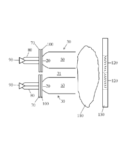
Figure 5 is a schematic cross-section showing an embodiment where, in use, two
adjacent electron sources 90, generate x-ray photons at the target material
70, the higher
energy x-ray photons pass through the filter material 100, are internally
reflected along
the collimating tapered holes 30 before passing through the subject matter 110
being
imaged and then arriving on adjacent elements 120 in a two-dimensional x-ray
sensor 130.
In this figure there is shown a one to one correspondence between the x-ray
sources and
the collimating holes, however, other ratios are contemplated such as a
plurality of x-ray
sources to one collimator, and one collimator to a plurality of targets (for
example four).
The interstitial elements 31 (i.e. the material lying between the holes 30)
act to
block any x-ray photons which pass between adjacent collimating tapered
entrance holes
20. For instance, the interstitial elements may absorb the x-rays. This
results in only x-
ray photons which have been guided down the collimating holes 30 in the
substrate
material 10 emerging approximately perpendicular to the collimator plane with
a
consequential improvement in the resulting image quality. In this regard, the
collimator
plane may be an imaginary plane lying perpendicular to the longitudinal axes
of the holes'
30 bores.
It is possible to add an additional thin layer of x-ray absorbing material at
the
output of the collimator hole 50, to absorb low energy x-ray photons. This
layer allows
for "hardening" or "stiffening" of the spectrum by absorbing the very low
energy x-rays
which do not contribute to the image formation but do increase the dose to the
patient
or target.
It is possible to use two or more of the collimator substrates 10, whereby the
substantially cylindrical output holes 30 of one x-ray collimator substrate 10
are aligned
with the entrance holes 20 of the adjacent x-ray collimator substrate 10 in
order to extend
the length of the collimation hole 30.
Other arrangements are also useful and contemplated. For example, it may be
useful to have a collimator hole comprising a short tapered region followed by
a gap (or
a larger diameter tube) which is terminated in a narrower hole. This
arrangement may be
effectively similar to the tapered section plus straight tube section
described above, but
allow simpler fabrication. However, it may be at the cost of less efficient
guiding of the
x-rays. Another arrangement that may be contemplated is a stack of several
holes with
varying diameter such that the overall profile is as previously described, but
whose
fabrication and construction are different. It may also be useful to replace
the
Date Recue/Date Received 2021-07-07
frustoconical portion with other shapes such as a linear taper (conical),
hyperbolic or
hemi-spherical section.
11
Date Recue/Date Received 2021-07-07