Note: Descriptions are shown in the official language in which they were submitted.
CA 2940152 2017-04-06
METHOD AND SYSTEM FOR POWER SIGNATURE SUPPRESSION IN MEMORY
DEVICES
,
CROSS REFERENCE TO RELATED APPLICATIONS
[0001] This application claims the benefit of priority of U.S. Provisional
Patent
Application No. 62/338,277, filed on May 18, 2016.
FIELD
[0002] The present disclosure relates generally to a memory device. More
particularly, the present disclosure relates to power signature suppression in
a memory
device.
BACKGROUND
[0003] It is well known that memory devices store data which is used by
other
systems to execute certain functions. Such data can be as simple as multimedia
files or
user readable documents, and the memory devices that store such data can be
non-
volatile memory such as portable USB drives, various known memory cards and
solid
state hard disk drives, by example. Such memory devices can be volatile memory
devices
such as dynamic random access memory (DRAM) or static random access memory
(SRAM) by example. In these cases, the memory devices can be standalone
semiconductor memory chips encapsulated in a package.
[0004] Another type of data is more sensitive, such as encryption keys or
passwords that are stored in a memory device and read out by a host system
when
needed. Such data can be stored in a memory device integrated with other
circuits, such
as in an application specific integrated circuit (ASIC) or other mixed circuit
system.
Alternately, a standalone memory device can be interconnected with a host
system on a
printed circuit board or in a multi-chip package to provide the storage
capability.
[0005] Naturally, such sensitive data should be secure from intentional and
unintentional discovery. While reverse engineering of semiconductor memory
devices
might be possible to discover the stored data, the cost to do so is very high
as it requires
specialized equipment to reveal physical circuit elements. Furthermore,
companies who
- 1 -
CA 02940152 2016-08-25
specialize in reverse engineering of semiconductor devices are unlikely to
engage in the illicit
act of unauthorized access of such sensitive data.
[0006] There has arisen a form of reverse engineering that can be
used to partially
determine the stored data in the memory device. This technique is referred to
as power
signature analysis, in which the power supply of the semiconductor memory
device or the
system the memory device is a part of, is monitored as the system is operated
to execute
various functions. The principle here is that particular data read out may
exhibit a power
consumption level that changes when different data states are read out,
eventhough the
actual data being read out is not known. So, as different read operations are
executed by the
memory device, power consumption will occur and the power supply will exhibit
variations in
its level. Patterns of the power supply variations can be correlated with
particular functions
over time (a clock signal), and when sufficient data is accumulated, analysis
of the patterns
may provide a clue as to the logic states of the data that is being accessed.
[0007] To illustrate the power signature problem with current memory
devices,
reference is made to Figure 1. Figure 1 is a schematic showing a known memory
array and
output path circuitry. The memory array is represented by bitlines BLO to BL7
and a wordline
WL, and it is assumed there is one memory cell connected at the intersection
of the wordline
WL with each bitline. Those skilled in the art understand that a memory array
can include
more than one wordline and the eight bitlines shown in Figure 1. The memory
array can
consist of non-volatile or volatile memory cells. Bitlines BLO-BL3 are
connected to a first
column selection circuit 10 represented by a multiplexor/demultiplexor symbol,
while bitlines
BL4-BL7 are connected to a second column selection circuit 12 represented by
multiplexor/demultiplexor symbol. Column selection circuits 10 and 12 are
controlled by
column selection signals (not shown) to couple one bitline to a databus line
DBO and DB1.
[0008] To read data, sense amplifiers 14 and 16 each compares voltages on
DBO
and DB1 respectively against a reference voltage VREF for output on ports QO
and Q1. The
VREF voltage is set to a voltage level to distinguish a bitline voltage as
being representative
of a logic "1" or a logic "0". This is more commonly known as single ended
sensing. Output
port QO outputs one bit of data, while output port 01 outputs a second bit of
data. To write
data, write drivers 18 and 20 receive write data from input ports DO and D1
for application to
DBO and DB1. The column selection circuits 10 and 12 are again controlled by
selection
signals to couple DBO and DB1 to selected bitlines, where WL is driven to
access the
- 2 -
CA 02940152 2016-08-25
memory cells to effect storage of the data to the memory cells connected to
the selected
bitlines. Elements 10, 12, 14 and 16 can be considered the output path
circuitry of Figure 1.
[0009] An example read operation timing diagram for the circuit of Figure 1 is
shown in
Figure 2, where successive bits are read out from output ports QO and Q1 at
each clock
cycle CLK. In this example, power consumption occurs in the memory array and
in the sense
amplifiers 14 and 16 each time QO (or Q1) transitions from a low logic state
to a high logic
state. Furthermore, different power consumption can occur during high to low
level
transitions versus low to high level transitions. As shown in Figure 2, there
may be one level
of power consumption when just a single output port transitions to the high
logic state, a
different level of power consumption when neither output port transitions to
the high logic
state, and yet another different level of power consumption when both output
ports transition
to the high logic state. While the instantaneous power consumption at a
particular clock cycle
can be monitored, the sequence of transitions of the output ports over
successive clock
cycles can also be used to determine a power signature of the memory device.
[0010] It is, therefore, desirable to provide a memory device configured to
suppress
any power signature during read operations.
SUMMARY
[0011] It is an object of the present disclosure to obviate or
mitigate at least one
disadvantage of previous semiconductor devices.
[0012] In a first aspect, the present disclosure provides a
semiconductor device
having a memory array and output path circuitry. The memory array has memory
cells
connected to bitlines and wordlines for providing a bit of data in a read
operation on at least
one bitline. The output path circuitry is coupled to the bitlines and
configured to sense the bit
of data from the at least one bitline. The output path circuitry has first and
second output
ports configured to be selectively driven to a reset voltage level in response
to a control
signal before the at least one bitline is sensed, and configured to output the
sensed bit of
data by driving one of the first and second output ports to a voltage level
corresponding to
the sensed bit of data. The reset voltage can be one of first voltage supply
level (VDD) and a
second voltage supply level (VSS).
[0013] According to a present embodiment, the memory array is
configurable to store
the bit of data in a single memory cell corresponding to one logic state, or
in at least two
memory cells corresponding to complementary logic states. In an aspect of the
present
- 3 -
CA 02940152 2016-08-25
embodiment, the memory array is configurable to store the bit of data in a
first pair of
memory cells corresponding to the complementary logic states, and a second
pair of memory
cells corresponding to the complementary logic states. Alternatively, the
memory array is
configurable to store the bit of data in a first pair of memory cells
corresponding to the
complementary logic states, and a second pair of memory cells corresponding to
the inverted
complementary logic states. In the present embodiment, a first portion of the
memory array is
configured to store data as single memory cell per bit and a second portion of
the memory
array is configured to store data in at least two memory cells per bit. In the
embodiment
where the memory array is configured to store the bit of data in a single
memory cell, the
control signal may be inhibited to prevent the first and the second output
ports from being
driven to a reset voltage level, and the output path circuitry outputs the
sensed bit of data on
the first output port and senses another bit of data from another bitline for
output on the
second output port. In the embodiment where the memory array is configured to
store the bit
of data in at least two memory cells, the output path circuitry includes reset
circuits each
configured to drive the first output port and the second output port to the
reset voltage level in
response to the control signal.
[0014] In the presently described embodiments, the reset circuits
include a first
transistor device connected between the first output port and the reset
voltage, and a second
transistor device connected between the second output port and the reset
voltage, each of
the first and second transistor devices having gate terminals for receiving
the control signal.
Alternately, the reset circuits include a first latch connected to the first
output port, and a
second latch connected to the second output port, each of the first and second
latches being
resettable by the control signal to drive the first output port and the second
output port to the
reset voltage.
[0015] According to another embodiment of the first aspect, the output path
circuitry
includes bitline selectors and a sense amplifier block. The bitline selectors
couple a first
bitline to a first databus and a second bitline to a second databus. The sense
amplifier block
is selectively operable in a single ended sensing mode and a differential
sensing mode for
sensing voltages on the first databus and the second databus, and configured
to drive the
first and second output ports to either the first voltage supply level (VDD)
or the second
voltage supply level (VSS). In this embodiment, the sense amplifier block
includes output
latch circuits each configured to drive the first output port and the second
output port to the
reset voltage level in response to the control signal.
- 4 -
CA 02940152 2016-08-25
[0016] Furthermore, the sense amplifier block can include a first
single ended sense
amplifier, a second single ended sense amplifier, a differential sense
amplifier and output
selectors. The first single ended sense amplifier is operable in the single
ended sensing
mode and configured to compare the first databus voltage to a reference
voltage to provide a
first single ended output. The second single ended sense amplifier is operable
in the single
ended sensing mode and configured to compare the second databus voltage to the
reference voltage to provide a second single ended output. The differential
sense amplifier is
operable in the differential sensing mode and configured to compare the first
databus voltage
to the second databus voltage to provide differential outputs. The output
selectors are
configured to couple the first single ended output and the second single ended
output to the
output latch circuits in the single ended sensing mode, and configured to
couple the
differential outputs to the output latch circuits in the differential sensing
mode.
[0017] Alternately, the sense amplifier block can include a first
differential sense
amplifier, a second differential sense amplifier and first reference
selectors. The first
differential sense amplifier has a first input connected to the first databus,
a second input
connected to a first reference node, and a first output. The second
differential sense amplifier
has a first input connected to the second databus, a second input connected to
a second
reference node, and a second output. The first output and the second output
are connected
to the output latch circuits. The first reference selectors couple a reference
voltage to the first
reference node and the second reference node in the single ended sensing mode,
and
couple the second databus to the first reference node and the first databus to
the second
reference node in the differential sensing mode.
[0018] In this embodiment, the reference selectors are further
configured to couple a
third bitline to the first reference node and to couple a fourth bitline to
the second reference
node in a second differential sensing mode, where the first bitline and the
third bitline carry
voltages corresponding to first complementary data, and the second bitline and
the fourth
bitline carry voltages corresponding to second complementary data. According
to the present
embodiment, the first complementary data and the second complementary data
represent
the same bit of data, and the first differential sense amplifier senses the
first complementary
data to output a true state of the bit of data and the second differential
sense amplifier
senses the second complementary data to output a complement of the true state.
[0019] According to yet another embodiment of the first aspect, the output
path circuitry
includes bitline selectors, a first differential sense amplifier, a second
differential sense
- 5 -
CA 02940152 2016-08-25
amplifier, a first output latch circuit and a second output latch circuit, and
reference selectors.
The bitline selectors are configured to selectively couple one of a first
bitline and a second
bitline to a first databus, and to selectively couple one of a third bitline
and a fourth bitline to a
second databus. The first differential sense amplifier has a first input
connected to the first
databus, a second input connected to a first reference node, and a first
output. The second
differential sense amplifier has a first input connected to the second
databus, a second input
connected to a second reference node, and a second output. The first output
latch circuit and
the second output latch circuit are each configured to drive the first output
port and the
second output port to the reset voltage level in response to the control
signal. The reference
selectors are configured to selectively couple one of a reference voltage, the
second bitline
and the second databus to the first reference node, and to selectively couple
one of the
reference voltage, the third bitline and the first databus to the second
reference node.
[0020] In a second aspect, the present disclosure provides method for
reading data
from a memory device. The method includes resetting differential outputs to a
first voltage
level; executing a read operation from a memory array of the memory device;
and, driving
one of the differential outputs to a second voltage level in response to the
data read from the
memory array. Resetting can include driving differential outputs to the first
voltage level, or
resetting can include resetting latch circuits connected to the differential
outputs. According
to an embodiment, executing the read operation includes asserting a wordline
of the memory
array, and activating at least one sense amplifier after asserting the
wordline. Resetting the
differential outputs can occur before activating the at least one sense
amplifier, and
concurrently to asserting the wordline.
[0021] Other aspects and features of the present disclosure will
become apparent to
those ordinarily skilled in the art upon review of the following description
of specific
embodiments in conjunction with the accompanying figures.
BRIEF DESCRIPTION OF THE DRAWINGS
[0022] Embodiments of the present disclosure will now be described,
by way of
example only, with reference to the attached Figures.
[0023] Fig. 1 is a circuit schematic of a memory array with output path
circuitry of the
prior art;
[0024] Fig. 2 is a timing diagram showing an example operation of the
output path
circuitry of Figure 1;
- 6 -
CA 02940152 2016-08-25
[0025] Fig. 3 is a block diagram of a memory device with power
signature
suppression, according to a present embodiment;
[0026] Fig. 4 is a timing diagram showing an example operation of the
output path
circuitry of Figure 3;
[0027] Fig. 5 is a circuit schematic of a memory array and output path
circuity,
according to a resent embodiment;
[0028] Fig. 6 is a timing diagram showing an example operation of the
output path
circuit of Figure 5;
[0029] Fig. 7 is a circuit schematic of a memory array and output
path circuity,
according to an alternate embodiment;
[0030] Fig. 8A, 8B, 8C, 8D, 8E and 8F are circuits schematics of a
memory array and
output path circuity shown operating in different modes, according to yet
another alternate
embodiment;
[0031] Fig. 9 is a flow chart of a method of operating the
embodiments shown in
Figures 8E and 8F;
[0032] Fig. 10 is a flow chart outlining a method of output path
circuitry power
signature suppression, according to a present embodiment; and
[0033]
[0034] Figs. 11A and 11B are circuits schematics showing alternate
output path
circuitry.
DETAILED DESCRIPTION
[0035] Generally, the present disclosure provides a method and system
for
suppressing power signature in a memory device during read operations. A
memory array
stores data in an even number of cells per bit, such as 2 cells per bit, where
complementary
data states are stored in each pair of cells. Differential access of the
memory array via the
bitlines suppresses power signature because the same power consumption occurs
regardless of the data being accessed. Data output buffers that provide
complementary data
to a downstream circuit system are reset to the same logic state during every
read operation
such that only one output buffer is ever driven to the opposite logic state in
each read cycle.
Hence the power consumption remains the same regardless of the data states
being read
out from the memory array and provided by the output buffers. This further
results in the
advantage of removing a detectable sequence of power signatures.
- 7 -
CA 02940152 2016-08-25
[0036] Furthermore the techniques described in the present
embodiments not only
hides a power signature within the memory device itself, but it also provides
a 'view' for co-
blocks to receive or write power-signature-independent data. In other words,
neighbouring
circuit blocks which are not part of the memory circuits but integrated on the
same chip can
also hide power signatures of complementary data they receive or provide if
they are
designed to do so within their structure.
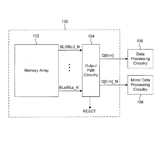
[0037] Figure 3 is a block diagram of a memory device with power
signature
suppression, according to a present embodiment. Memory device 100 includes a
memory
array 102 having memory cells connected to bitlines and wordlines, where at
least two
memory cells are used to store a single bit of data as complementary data
states or each
memory cells stores a single bit of data. The memory cells can be volatile or
non-volatile
memory cells. Using two cells to store a single bit of data as complementary
logic states is
well known in the art, and therefore not discussed in further detail.
Accordingly, the physical
bitlines are logically referred to as complementary bitlines BLO/BLO_N to
BLp/BLp_N, where
"p" is an integer number representing the last bitlines and "N" designates a
complementary
bitline. Therefore voltages on each pair of BUBL_N bitlines represents a
single bit of data.
Output path circuitry 104 outputs read data from the memory array 102 onto
differential ports
Q[0:m]/Q[0:m]_N, where "m" is an integer number representing the last output
ports, and "N"
designates a complementary output port. As will be described in further detail
later, output
path circuitry 104 employs differential sensing for comparing voltages of
complementary
bitlines to each other or single ended sensing for comparing voltages of
bitlines to a
reference voltage.
[0038] Therefore each pairing of Q/Q_N output ports provides output
voltages
representing a single bit of data. The output path circuitry 104 receives a
reset signal RESET
that is activated at a specific time during a read operation from the memory
array 102 to
suppress any power signature during outputting of data from the Q/Q_N output
ports. Further
details of where and how this reset signal is used by output path circuitry
104 is discussed in
further detail later.
[0039] The memory device 100 will include other circuits that are
required to ensure
proper operation, but these are not shown in Figure 3 as they are not relevant
to the present
embodiments. The memory device 100 can be a stand-alone semiconductor chip or
it can be
integrated on a system on a chip having other downstream circuits. Example
downstream
circuits include data processing circuitry 106 that receives the true data and
mirror data
- 8 -
CA 02940152 2016-08-25
processing circuitry 108 configured to be the same as data processing
circuitry 106 that
receives the complement of the true data.
[0040] According to the present embodiments, the memory array 102 and
output path
circuitry 104 do not exhibit any power signature that could be used to help
discern the data
being output during any read operation. Regardless of the state of data being
read out, the
memory array 102 consumes the same power and the output path circuitry 104
consumes
the same power since there is always logic "1" and logic "0" output in each
read cycle. To
further suppress power signature in a larger integrated system, the mirror
processing circuitry
108 functions the same way as the actual data processing circuitry 106 so that
one of the two
circuits 106 or 108 is always operating regardless of the output data.
[0041] Figure 4 is a simplified timing diagram showing power signature
suppression
by the output path circuitry 104, according to a present embodiment. It is
assumed that
complementary states of data are read out from the memory array 102,
differentially sensed
and output by output path circuitry 104 on complementary ports Q and Q_N in
synchronization with a clock. Also shown in Figure 4 is the signal trace for
the reset signal
RESET of Figure 3. Starting on the left side of Figure 4, the first read
operation starts at
rising CLK edge 110, which initiates the read sequence that can include any
required bitline
precharging, wordline activation and sensing.
[0042] A first RESET pulse is issued shortly after rising edge 110 to
cause both Q
and Q_N output ports to be driven to a reset state of a first voltage level,
in this example
VSS, which represents a logic "0" state. Concurrently with or after the RESET
pulse is
issued, sensing of the bitline data is initiated and the output path circuitry
104 eventually
drives Q and Q_N with sensed data. More specifically, Q is driven to a second
voltage level,
in this example VDD, which represents a logic "1" state. As it is the
complement of the Q,
Q_N is driven to the first voltage level of VSS. However, since Q_N was
already reset to the
VSS level due to RESET, there is no change to the level of Q_N relative to the
previous reset
state. This process repeats for the next four data read operations. It is
clear that for each of
the remaining four read operations, only one of Q or Q_N is driven to the
second voltage
level of VDD, and there are exactly two output buffer transitions within each
read cycle. The
two transitions are noted for each clock cycle in Figure 4. Therefore, there
is no power
signature between the different data states being read out, or relative to any
previous data
states being read out.
- 9 -
CA 02940152 2016-08-25
[0043] Having memory array 102 configured to store data in two cells
reduces the
total storage capacity relative to a configuration where a data is stored in a
single cell. In this
particular example, the total storage capacity is reduced by 50%. Furthermore,
the output
data width is reduced by 50%. For example, a 64Mb memory device configured for
single cell
per bit storage having a data width of 32 bits will have QO to Q31 output
ports. Assuming the
memory array and number of internal data buses remains unchanged, another
version of the
memory device configured for two cell per bit storage will store up to 32Mb
and have a data
width reduced to 16 bits for output on ports Q0/QO_N to Q15/Q15_N. While some
applications do not require secure data storage and prefer high total storage
capacity and
high bandwidth, other applications may require secure data storage with power
signature
suppression as a higher priority.
[0044] According to a present embodiment, the memory array 102 can be
configured
to store data in either single cell per bit mode, two cell per bit mode, or
both while the output
path circuitry 104 can be selectively configurable to receive, sense and
output received
bitline data for either single cell per bit mode or the two cell per bit mode.
This allows for a
single memory device to be manufactured that can be used in different
applications. A further
enhancement of the two cell per bit mode is a two cell per bit mode with
redundancy.
[0045] Commonly owned patent US 8,213,211 discloses a memory array
with bitlines
and wordlines which can store data as single cell per bit or two or more cells
per bit.
Reference may be made to teachings of that application to see example memory
array
configurations allowing for different numbers of cells per bit storage modes.
The following
description is directed to embodiments of the output path circuitry 104 for
receiving bitline
voltages in either the single or two cell per bit storage modes.
[0046] Figure 5 is a circuit schematic of a first embodiment of
output path circuitry
104. The bitlines BLO-BL7 and the wordline WL are representative of the memory
array 102.
The output path circuitry 104 of the present embodiment includes bitline
selectors 200 and
202 each connected to a respective group of bitlines, single ended sense
amplifiers 204 and
206, a differential sense amplifier 208, output selectors 210 and 212, and
output buffers 214
and 216 connected to output ports Q and Q_N. The output buffers 214 and 216 of
the
present examples are shown as output latch circuits. Write drivers 218 and 220
are not part
of the output path circuitry 104, but are shown for completeness. This
arrangement of
components shown in the dashed line of box 104 is repeated for all other
groups of bitlines of
memory array 102, and it is assumed that memory array 102 is configured to
have an even
- 10-
CA 02940152 2016-08-25
number of such bitline groups. Following is a more detailed explanation of the
previously
mentioned components.
[0047] The memory array 102 is configured to store data as single cell
per bit or two
cell per bit. Activation of a wordline in a read operation accesses all cells
connected to it.
Bitline selectors 200 and 202 function as column select circuits, and receive
the same
decoded column address signals (not shown) for each selecting one bitline to
connect to
respective databuses DB and DB_N. There can be any number of bitlines
connected to each
of bitline selectors 200 and 202. Databus DB is connected to one input of
single ended sense
amplifier 204 and connected to a first input of differential sense amplifier
208. The other input
of single ended sense amplifier 204 receives a reference voltage VREF.
Similarly, databus
DB_N is connected to one input of single ended sense amplifier 206 and
connected to a
second input of differential sense amplifier 208. The other input of single
ended sense
amplifier 206 receives the reference voltage VREF.
[0048] The output of single ended sense amplifier 204 is provided to a
first input of
output selector 210 and a first output of differential sense amplifier 208 is
provided to a
second input of output selector 210. Similarly, the output of single ended
sense amplifier 206
is provided to a first input of output selector 212 and a second output of
differential sense
amplifier 208 is provided to a second input of output selector 212. All the
sense amplifiers
shown in Figure 5 are enabled by a sense enable signal SENSE to compare its
inputs and
for providing a corresponding resulting output. Output selectors 210 and 212
receive a mode
control signal MODE to select which of its inputs to couple to latch 214 and
216 respectively
via the intermediate outputs q and q_N. The output selectors 210 and 212 are
shown having
input positions labelled with numerals 1 and 2, such that signal MODE in one
state selects
inputs 1 while signal MODE in another state selects inputs 2, for passage to
the output.
While not labelled with inputs 1-4, the bitline selectors 200 and 202 are also
similarly
configured to select the same input in response to the same decoded column
address
signals. From this point forward, any selector having numbered input positions
should be
understood to function as described above. Each output latch circuit 214 and
216 receives a
reset signal RESET and are connected to output ports Q and Q_N. The write
circuitry
consisting of write drivers 218 and 220 receive write data from input ports D
and D_N for
driving onto DB and DB_N respectively.
[0049] The output path circuitry 104 embodiment of Figure 5 can
operate in either a
single ended mode or a differential mode, depending on how data is stored in
memory array
-11 -
CA 02940152 2016-08-25
102. Following is an example of the differential mode read operation where
power signature
is suppressed, with reference to the timing diagram of Figure 6. The timing
diagram of Figure
6 includes signal traces for all the signals shown in Figure 5. The signal
traces for the
bitlines, databuses and output ports generically represents the cases where
the stored data
is a logic "1" or logic "0".
[0050] In the present example, it is assumed that the memory array
consists of anti-
fuse memory cells, such as the ones disclosed in commonly owned patent USP
8,213,211 by
example, and that two memory cells store one bit of data as complementary data
states.
Therefore memory cells connected to bitlines BLO-BL3 store one state of the
bits and bitlines
BL4-BL7 store the complementary state of the bits. In the present example, it
is assumed
that BLO and BL4 are selected for connection to respective databuses DB and
DB_N, which
is shown in Figure 5 by the "X" positioned over the intersecting lines of BLO,
BL4 and WL.
Also, control signal MODE is set to one logic state to enable output selectors
210 and 212 to
select only the outputs from differential sense amplifier 208 to couple to
output latch circuits
214 and 216. It is further assumed that the bitlines and the databuses DB/DB_N
are
precharged to VSS with precharge circuitry (not shown).
[0051] The read operation begins shortly after the rising edge of CLK,
where WL is
activated. At about this same time, the RESET signal is asserted as a pulsed
signal. The
RESET signal causes all the output latch circuits 214 and 216 to reset to the
VSS voltage
level. It is noted that RESET can be asserted anytime before the sense
amplifiers are
triggered, or enabled, which in the present embodiments is before the rising
edge of SENSE.
The activated wordline causes one of the selected bitlines precharged to VSS
to rise to a
high voltage, while the other bitline remains at about the VSS precharge
voltage level. At a
predetermined time, the bitline selectors 200 and 202 are activated by column
select signals
to couple the selected bitlines to DB and DB_N, at which point one of DB or
DB_N will rise to
a high voltage level. This predetermined time can be calibrated based on when
the sense
amplifiers 204, 206 and 208 are to be activated by SENSE, to allow sufficient
voltage to
develop on DB/DB_N. In the present example, the bitline selectors 200 and 202
can be
activated concurrent with or after the rising edge of CLK or WL. At the
falling edge of CLK,
the SENSE is asserted to turn on all the sense amplifiers.
[0052] The inputs to differential sense amplifier 208 are sensed and
the voltages on
DB and DB_N are driven to complementary high and low voltage levels, where one
of DB
and DB_N will reach the full voltage rail level when the sense amplifier 208
is activated. The
- 12 -
CA 02940152 2016-08-25
complementary outputs of differential sense amplifier 208 are then latched by
output latch
circuits 214 and 216 for output on the Q and Q_N ports. Because the output
latch circuits
214 and 216 were reset after the read operation was initiated and prior to
sensing by
differential sense amplifier 208, only one output latch circuit 214 or 216
ever drives its output
to the high logic level. The next read cycle would commence on the next rising
edge of CLK,
and the process repeats as previously described for the first read operation.
Therefore
suppressed power signature is exhibited regardless of the data being accessed
and the
sequence of data being read out.
[0053] In the presently shown embodiment of Figure 5, the same SENSE
signal is
used to enable the single ended sense amplifiers 204, 206 and the differential
sense
amplifier 208. In an alternate embodiment, the MODE signal can be logically
combined with a
master sense signal to generate separate two distinct sense signals ¨ one for
enabling just
the single ended sense amplifiers 204, 206 and another for enabling just the
differential
sense amplifier 208.
[0054] To operate the output path circuitry 104 in the single ended mode,
the MODE
signal is changed to a logic state corresponding to single ended operation so
that only the
outputs of single ended sense amplifiers 204, 206 are coupled to output latch
circuits 214
and 216. In the single ended mode, the RESET signal is not used and remains in
an inactive
state. In the single ended mode, databuses DB and DB_N are now logically
treated as DBO
and DB1, while output ports Q and Q_N are now logically treated as QO and Q1.
This is
because the data read from the cells connected to bitlines BLO and BL4 now
store
independent data bits.
[0055] The output path circuitry embodiment of Figure 5 uses dedicated
single ended
and differential sense amplifiers. According to the alternate embodiment of
Figure 7, a
differential sense amplifier can be used for both single ended and
differential sensing
operations.
[0056] Figure 7 is a circuit schematic of a second embodiment of
output path circuitry
104. The bitlines BLO-BL15 and the wordline WL are representative of the
memory array
102. The output path circuitry 104 of the present embodiment includes first
stage bitline
selectors 300, 302, 304 and 306 each connected to a respective group of
bitlines, second
stage bitline selectors 308 and 310, differential sense amplifiers 312 and 314
having outputs
q and q_N, reference selectors 316 and 318, and output latch circuits 320 and
322
connected to output ports Q and CLN. In variations of the present embodiment,
the output
- 13-
CA 02940152 2016-08-25
latch circuits 320 and 322 can be integrated together with the differential
sense amplifiers
312 and 314 respectively. Write drivers 324 and 326 are not part of the output
path circuitry
104, but are shown for completeness. This arrangement of components shown in
the dashed
line of box 104 is repeated for all other groups of bitlines of memory array
102, and it is
assumed that memory array 102 is configured to have an even number of such
bitline
groups. Similar to the embodiment of Figure 5, there can be any number of
bitlines
connected to each of the first stage bitline selectors. The elements shown in
the dashed line
of box 104 are collectively referred to as a mixed sensing block, which can be
operated in the
single ended or differential sensing modes. Within the mixed sensing block are
first and
second single ended sensing units. The first such unit consists of elements
300, 302, 308,
316, 312 and 320. The second such unit consists of elements 304, 306, 310,
318, 314 and
322.
[0057] Following is a more detailed explanation of the previously
mentioned
components.
[0058] The memory array 102 is configured to store data as single cell per
bit or two
cell per bit. Activation of a wordline in a read operation accesses all cells
connected to it.
First stage bitline selectors 300, 302 and second stage bitline selector 308
function as
column select circuits, and receive decoded column address signals (not shown)
for
selecting one bitline of BLO to BL7 to connect to databus DB. Similarly, first
stage bitline
selectors 304, 306 and second stage bitline selector 310 receive the same
decoded column
address signals (not shown) for selecting one bitline of BL8 to BL15 to
connect to databus
DB_N.
[0059] Databus DB is connected to one input of differential sense
amplifier 312 and
connected to a first input of reference selector 318. Databus DB_N is
connected to one input
of differential sense amplifier 314 and connected to a first input of
reference selector 316.
Reference selectors 316 and 318 each have a second input receiving a reference
voltage
VREF, and is controlled by signal MODE. The output of reference selector 316
is provided to
a second input of differential sense amplifier 312 and the output of reference
selector 318 is
provided to a second input of differential sense amplifier 314. Differential
sense amplifier 312
has its true output connected to output latch circuit 320, while differential
sense amplifier 314
has its true output connected to output latch circuit 322. The complementary
outputs of the
differential sense amplifiers 312 and 314 are not used in this embodiment.
- 14 -
CA 02940152 2016-08-25
[0060] All the differential sense amplifiers shown in Figure 7 are
enabled by a sense
enable signal SENSE to compare its inputs and for providing a corresponding
resulting
output. Depending on the state of MODE, the differential sense amplifiers will
compare the
databus voltage on their true inputs to either VREF or to the other databus
voltage. For
example, differential sense amplifier 312 either compares DB from its true
input to VREF or
to DB_N. Each output latch circuit 320 and 322 receives a reset signal RESET
and are
connected to output ports Q and Q_N. The write circuitry consisting of write
drivers 324 and
326 receive write data from input ports D and D_N for driving onto DB and DB_N
respectively.
[0061] The output path circuitry 104 embodiment of Figure 7 can operate in
either a
single ended mode or a differential mode, in a manner very similar to that of
Figure 5. In the
embodiment of Figure 7, it is assumed that only one bitline of the first group
of bitlines BLO-
BL7 is coupled to DB and only one bitline of the second group of bitlines BL8-
BL15 is
coupled to DB_N via the first and second stage bitline selectors for both
differential and
single ended modes. Two stage selection of bitlines is well known in the art.
[0062] In the differential mode of operation, it is assumed memory
cells connected to
bitlines BLO-BL7 store one state of the bits and bitlines BL8-BL15 store the
complementary
state of the bits. In the present example, BLO and BL8 are accessed which
means that the
cells they are connected to store complementary states of a bit of data. In
Figure 7, the "X"
positioned over the intersecting lines of BLO, BL8 and WL shows this pairing
of bitlines for
the differential mode of operation. Of course, other bitline pairings are
possible in the
embodiment of Figure 7. For example, the triangle shapes at the cross points
of BL7, BL15
and WL show another valid pairing of bitlines for the differential mode of
operation, as does
do the square shapes at the cross points of BL4, BL12 and WL.
[0063] The read operation sequence is the same as shown in the timing
diagram of
Figure 6. During a read operation, RESET is asserted to drive Q and Q_N to
VSS. DB and
DB_N carry voltages corresponding to complementary data states of the bit
accessed from
the memory array 102. Reference selectors 316 and 318 are controlled by MODE
in the
differential mode to couple DB_N to differential sense amplifier 312 and to
couple DB to
differential sense amplifier 314. The differential sense amplifiers 312 and
314 are activated
by asserting sense signal SENSE. The sensed true outputs from each
differential sense
amplifier is then provided to output latch circuits 320 and 322, where only
one drives its
output to the high logic level. Accordingly, each single ended sensing unit
senses a voltage
- 15-
CA 02940152 2016-08-25
of one bitline connected to its first stage bitline selectors and one bitline
connected to first
stage bitline selectors of the second single ended sensing unit, and vice
versa.
[0064] The single ended mode of operation differs only in that the
memory cells
connected to BLO and BL8 each store their own bit of data, and MODE is set to
a different
logic state such that the voltage on DB is compared to VREF and the voltage on
DB_N is
compared to VREF. Once again, RESET is not asserted in the single ended mode
of
operation. Accordingly, each single ended sensing unit senses a voltage of one
bitline
connected to its first stage bitline selectors.
[0065] In the embodiment of Figure 7, single ended sensing or
differential sensing
with differential output modes of operation are possible. According to an
alternate
embodiment to the embodiment of Figure 7, the output path circuitry 104 can be
configured
to provide single ended sensing, differential sensing with differential
output, and differential
sensing with single ended output.
[0066] Figure 8A is a circuit schematic of a third embodiment of
output path circuitry
104. The elements shown in the circuit of Figure 8A are similar to those shown
in the
embodiment of Figure 7, and therefore the same reference numbers designate the
same
elements which function in the same ways as previously described for Figure 7.
The
elements shown in the dashed line of box 104 are collectively referred to as a
mixed sensing
block, which can be operated in the single ended or differential sensing
modes. Within the
mixed sensing block are first and second single ended sensing units. The first
such unit
consists of elements 300, 302, 308, 400, 312 and 320. The second such unit
consists of
elements 304, 306, 310, 402, 314 and 322.
[0067] The circuit differences between the embodiments of Figures 7
and 8A are now
described in detail.
[0068] In the embodiment of Figure 8A, the memory array 102 is the same as
the
memory array 102 described in the embodiment of Figure 7. For the purposes of
the
following discussion, bitlines BLO-BL3 are referred to as a first bitline
group, bitlines BL4-BL7
are referred to as a second bitline group, bitlines BL8-BL11 are referred to
as a third bitline
group, and bitlines BL12-BL15 are referred to as a fourth bitline group. In
the embodiment of
Figure 8A, reference selectors 400 and 402 replace reference selectors 316 and
318 of
Figure 7. The first reference selector 400 has a first input receiving a
reference voltage
VREF, a second input connected to DB_N for receiving its voltage, and a third
input
connected to the output of first stage bitline selector 302 for receiving a
voltage of one of
- 16-
CA 02940152 2016-08-25
bitlines BL4-BL7. Similarly, second reference selector 402 has a first input
receiving a
reference voltage VREF, a second input connected to DB for receiving its
voltage, and a third
input connected to the output of first stage bitline selector 304 for
receiving a voltage of one
of bitlines BL8-BL11. Reference selector 400 receives control signals MODE1
and MODE2
for selecting one of its three inputs to couple to an input of differential
sense amplifier 312.
Reference selector 402 receives the same control signals MODE1 and MODE2 for
selecting
one of its three inputs to couple to an input of differential sense amplifier
314. MODE1 and
MODE2 can be decoded by logic circuits within reference selectors 400 and 402
to perform a
1 of 3 selection operation, as should be well understood by those skilled in
the art.
[0069] The operation modes of the present embodiment are now described in
further detail
with reference to Figures 8A, 8B, 8C, 8D and 8E. Figures 8A, 8B, 8C, 8D and 8E
show
identical circuitry, except for annotations showing example bitlines which are
accessed in the
different modes of operation.
[0070] The single ended mode of operation in Figure 8A is the same as
previously described
for the embodiment of Figure 7, except that the MODE1 and MODE2 signals are
set to
enable reference selectors 400 and 402 to couple VREF to the respective inputs
of
differential sense amplifiers 312 and 314. Therefore, a bitline from the first
bitline group of
BLO-BL3 or a bitline from the second bitline group of BL4-BL7 is coupled to DB
for sensing
relative to VREF. Similarly a bitline from the third bitline group of BL8-BL11
or a bitline from
the fourth bitline group of BL12-BL15 is coupled to DB_N for sensing relative
to VREF. In a
specific example, the first and second stage bitline selectors 300, 302 and
308 couple BLO to
DB, while the first and second stage bitline selectors 304, 306 and 310 couple
BL8 to DB_N.
For the presently shown embodiments, it is assumed that the column decoding is
replicated
for the first stage bitline selectors 300, 302, 304, 306 and the column
decoding is replicated
for the second stage bitline selectors 308 and 310. Accordingly, each single
ended sensing
unit senses a voltage of one bitline connected to its first stage bitline
selectors. For ease of
reference, the "X" at the cross point of BLO and WL represents a memory cell
storing singled
ended data which ultimately appears at the input of differential sense
amplifier 312, and the
white box at the cross point of BL12 and WL represents a memory cell storing
unrelated
singled ended data which ultimately appears at the input of differential sense
amplifier 314.
[0071] The differential sensing with differential output mode is shown
by example in
Figure 8B, and is the same as the differential mode described for the
embodiment of Figure
7, except that the MODE1 and MODE2 signals are set to enable reference
selectors 400 and
- 17-
CA 02940152 2016-08-25
402 to couple DB_N to differential sense amplifier 312 and to couple DB to
differential sense
amplifier 314. Therefore, a bitline from the first or second bitline groups is
compared to a
bitline from the third or fourth bitline groups by both differential sense
amplifiers 312 and 314.
In a specific example, BLO and BL12 are selected as the complementary bitlines
for coupling
to DB and DB_N respectively, for differential sensing and output as
differential outputs Q and
Q_N. As shown in Figure 8B, a white box at the cross point of BLO and WL
represents a
memory cell storing one data state and a black box at the cross point of BL12
and WL
represents a memory cell storing an opposite data state to the white box,
representing the
differential data which ultimately appears at the inputs of differential sense
amplifiers 312 and
314. Accordingly, each single ended sensing unit senses a voltage of one
bitline connected
to its first stage bitline selectors and one bitline connected to first stage
bitline selectors of
the second single ended sensing unit, and vice versa.
[0072] For the previously described differential sensing with
differential output mode,
one memory cell storing true data is connected to a bitline in either the
first or second bitline
groups, while the other memory cell storing complementary data is connected to
a bitline in
either the third or fourth bitline groups. In this mode of operation, the
RESET signal is used
as discussed in the previous embodiments.
[0073] Figure 8C illustrates another type of differential sensing
mode, according to a
present embodiment. In the presently described differential sensing with
single ended output
mode, one bit of data is stored as two cells per bit, but only a single output
port provides the
sensed data. One memory cell of a pair of memory cells storing complementary
data for one
bit is connected to a bitline in the first bitline group, while the other
memory cell of the pair of
memory cells is connected to a bitline in the second bitline group. Similarly,
one memory cell
of a pair of memory cells storing complementary data for one bit is connected
to a bitline in
the third bitline group, while the other memory cell of the pair of memory
cells is connected to
a bitline in the fourth bitline group.
[0074] In this two cell per bit storage configuration in memory array
102, MODE1 and
MODE2 signals can be set to enable reference selector 400 to couple the output
of first
stage bitline selector 302 to one input of differential sense amplifier 312,
while the first and
second stage bitline selectors 300 and 308 couple a bitline from the first
bitline group to the
other input of differential sense amplifier 312. By example, a white box at
the cross point of
BL1 and WL and a black box at the cross point of BL5 and WL represents the
memory cells
storing the differential data which ultimately appears at the inputs of
differential sense
- 18-
CA 02940152 2016-08-25
amplifier 312. Similarly, reference selector 402 is enabled by MODE1 and MODE2
to couple
the output of third stage bitline selector 304 to one input of differential
sense amplifier 314,
while the first and second stage bitline selectors 306 and 310 couple a
bitline from the fourth
bitline group to the other input of differential sense amplifier 314. By
example, a black
triangle at the cross point of BL9 and WL represents one data state and a
white triangle at
the cross point of BL13 and WL represents an opposite data state to the white
triangle, which
are the memory cells storing the differential data that ultimately appears at
the inputs of
differential sense amplifier 314. Under these conditions, each differential
sense amplifier 312
and 314 compares different pairs of differential bitlines to each other and
outputs a single
ended result from its respective output port. Accordingly, the Q and Q_N
outputs do not have
to have opposite logic states to each other. As for the previously described
single ended
sensing embodiments, the RESET signal is not asserted during any part of the
read
operation. Accordingly, each single ended sensing unit differentially senses
voltages of
complementary bitlines connected to its first stage bitline selectors to
provide a single ended
result.
[0075] Figure 8D illustrates a variation of the differential sensing
with single ended
output mode of 8C. In the differential sensing with single ended output mode,
one bit of
information is stored as complementary data states in cells connected to BL1
and BL5, while
another different bit of information is stored as complementary data states in
cells connected
to BL9 and BL13. In the present redundant differential sensing mode, the same
bit of
information is stored in two pairs of cells each storing complementary data
states. For
example, a white "A" box at the cross point of BL1 and WL is true data and a
black "A" box
at the cross point of BL5 and WL can be the complement data, where both
represents the
memory cells storing the differential data corresponding to a first bit of
information. Similarly,
a black "B" box at the cross point of BL9 and WL is true data and a white "B"
box at the cross
point of BL13 and WL can be the complement data, where both represents the
memory cells
storing the differential data of a second bit of information being the same as
the first bit of
information. The data states of the two white boxes are the same while the
data states of the
two black boxes are the same. Accordingly, the outputs Q and Q_N should have
the same
logic states.
[0076] With this data storage configuration, redundancy can be
provided for mission
critical applications. In a read operation, the complementary "A" data are
compared to each
other and the complementary "B" data are compared to each other. To do this,
the second
-19-
CA 02940152 2016-08-25
stage bitline selectors 308 and 310 are controlled to couple BL1 and BL13 to
DB and DB_N
respectively, and reference selectors 400 and 402 can be controlled by MODE1
and MODE2
to couple BL5 to sense amplifier 312 and BL9 to sense amplifier 314. In this
read mode, Q
and Q_N should provide the same output if the complementary data was properly
programmed to the memory cells connected to bitline pairs BL 1/BL5 and
BL9/BL13.
[0077] If during testing of the memory of Figure 8D after
programming, it is
determined that certain memory cells could not be properly programmed, they
are deemed
defective and their location is noted for redundancy programming. More
specifically, it would
be known which of Q and Q_N provides data from a defective memory cell.
Therefore in one
embodiment of redundancy programming, additional switch circuitry similar to
bitline selector
circuit 308 connected to receive the Q and Q_N outputs can be programmed to
output the
non-defective data to any downstream circuit. For example, the signals
controlling this
additional switch circuitry can be set through fuse programming, or other
programming
techniques known in the art. Alternately, if the Q and Q_N outputs are
different, both outputs
can be ignored and a new address is used for both.
[0078] While the previous embodiment of Figure 8D provides single
ended outputs
which can exhibit a power signature, the same circuit can be used to provide
redundant
differential sensing with differential outputs to minimize power signature, as
shown by
example in the embodiment of Figure 8E.
[0079] In the redundant differential sensing with differential outputs
operation of
Figure 8E, one bit of information is stored as complementary data states in
cells connected
to BL1 and BL5, while another different bit of information is stored as
complementary data
states in cells connected to BL9 and BL13. It should be noted that the data
storage
configuration of the "B" boxes is swapped relative to the configuration shown
in the
embodiment of Figure 8D. As in the embodiment of Figure 80, the data states of
the two
white boxes are the same while the data states of the two black boxes are the
same.
[0080] With this data storage configuration of Figure 8E, redundancy
can be provided
for mission critical applications. In the read mode, the white "A" data is
compared to the black
"A" data at sense amplifier 312 and white "B" data is compared to the black
"B" data at sense
amplifier 314. To do this, the second stage bitline selectors 308 and 310 are
controlled to
couple BL1 and BL13 to DB and DB_N respectively, and reference selectors 400
and 402
can be controlled by MODE1 and MODE2 to couple BL5 to sense amplifier 312 and
BL9 to
sense amplifier 314. In this read mode, Q and Q_N should be complementary data
states if
- 20 -
CA 02940152 2016-08-25
the complementary data was properly programmed to the memory cells connected
to bitlines
BL1 and BL13. This can be referred to as a simple secure-redundant
differential mode of
operation.
[0081] Another alternate mode of operation for the circuit embodiment
of Figure 8E
having the same data storage pattern is shown in Figure 8F. With this data
storage
configuration, redundancy can be provided for mission critical applications.
In a first read
mode, the white "A" data is compared to the black "B" data at sense amplifiers
312 and 314.
To do this, the second stage bitline selectors 308 and 310 are controlled to
couple BL1 and
BL13 to DB and DB_N respectively, and reference selectors 400 and 402 can be
controlled
by MODE1 and MODE2 to couple DB to sense amplifier 314 and DB_N to sense
amplifier
312. In this read mode, Q and Q_N should be complementary data states if the
complementary data was properly programmed to the memory cells connected to
bitlines
BL1 and BL13.
[0082] In a second read mode, the black "A" data is compared to the
white "B" data
at sense amplifiers 312 and 314. To do this, the second stage bitline
selectors 308 and 310
are controlled to couple BL5 and BL9 to DB and DB_N respectively, and
reference selectors
400 and 402 can be controlled by MODE1 and MODE2 to couple DB to sense
amplifier 314
and DB_N to sense amplifier 312. With reference to Figure 8E, the black "A"
data would
appear on the "+" input of sense amplifier 312 and at the "2 input of sense
amplifier 314,
while the white "B" data would appear on the "2 input of sense amplifier 312
and the"+" input
of sense amplifier 314. In this routing configuration of the bitline data to
sense amplifiers 312
and 314, the Q and Q_N outputs should still be complementary data states if
the
complementary data was properly programmed to the memory cells connected to
bitlines
BL5 and BL9. It should be noted that the Q and Q_N outputs will have data
states that are
inverted relative to the first read mode, therefore downstream circuits can be
used to re-
invert the data states.
[0083] Therefore, the embodiment of Figure 8F can be operated in
either of the two
different described modes in order to provide redundant and secure
differential output data
as no power signature is produced. In both read modes, the same stored data is
sensed by
two different sense amplifiers, but each read mode senses a different pairing
of stored data.
In a further variation of the embodiment of Figure 8F, the circuit can be
operated using the
two previously described modes to provide time-based redundancy, as is now
described with
reference to the flow chart of Figure 9. It is assumed that the redundant data
has been
- 21 -
CA 02940152 2016-08-25
programmed as shown in Figures 8E and 8F. Starting at 500, the first read mode
as shown
in the embodiment of Figure 8E is executed to provide the data on the
differential outputs Q
and Q_N. This first read data can be temporarily stored in first registers
(not shown) which
are coupled to the Q and Q_N outputs. Following at 502 the method enters a
wait state, and
then the second read mode as shown in the embodiment of Figure 8F is executed
to provide
the data on the same differential outputs Q and Q_N. This second read data can
be
temporarily stored in second registers (not shown) which are coupled to the Q
and Q_N
outputs.
[0084] Proceeding to 506 the differential data stored in the first
registers and second
registers can be compared to each other using well-known logic to determine if
they match or
mismatch. It should be noted that the complementary data carried by Q and Q_N
in the first
read operation versus the second read operation are inverted relative to each
other,
therefore the comparison logic should be configured to take this into account.
If the data
matches, then the method ends at 508 and all 4 stored "A" and "B" bits of data
are deemed
to be correct. Otherwise, the method proceeds to 510 where at least one of the
4 stored bits
is deemed to be incorrectly stored, which may be indicative of defective
memory cell. At this
point, additional preset algorithms can be executed to identify which of the
pairs of stored
complementary data bits should not be used.
[0085] Accordingly, these two described read modes can be used to
validate the
programming of the complementary "A" and complementary "B" data by checking
that the Q
and Q_N outputs are complementary in the first read mode, and complementary
but inverted
in the second read mode relative to the first read mode. In both read modes,
power signature
is minimized by inserting the RESET signal in the manner described for the
previous
embodiments. The previously described method of Figure 9 can be executed any
number of
times during the life of the memory system to check the stored data.
[0086] The previously described embodiments of the output path
circuitry 104 shown
in Figures 5, 7 and 8A-8E can be configured for one operating mode for the
entire memory
array. For example, all the mixed sensing blocks can be configured for
operating in the
differential sensing mode with differential output and any power signature
from the memory
device is minimized by asserting the RESET signal as previously described.
Alternately,
some mixed sensing blocks can be configured for one mode of operation while
other mixed
sensing blocks can be configured for a different mode of operation. For the
embodiments of
8 Figures 8A-8E, four different modes of operation can be reserved for
different parts of the
- 22 -
CA 02940152 2016-08-25
memory array. A different part of a memory array can refer to one or more rows
of memory
cells connected to particular wordlines, or a range of wordlines. Therefore
the previously
described MODE signals can be decoded with one or more row addresses for
automatic
assertion to the appropriate logic level(s) that sets the desired mode of
operation. Such
flexibility allows the memory array to store a large amount of data, while
allowing for storage
of a small amount of secure data, such as a code, encryption key, or any other
data for which
detection by power signature is undesired.
[0087] To summarize, several of the presently described embodiments
provide power
signature suppression when data is stored as two cells (or more) per bit and
the output path
circuitry provides sensed complementary data on output ports. The flow chart
of Figure 10
summarizes a method for power signature suppression in a semiconductor memory
device.
The method assumes that data is stored differentially in a memory array, in at
least two cells
per bit. The method of Figure 10 starts at 600 by resetting differential or
complementary
output ports, such as Q and Q_N shown in the previously described embodiments,
to a first
voltage level. This can be a VSS voltage level or another voltage level
corresponding to
another possible data state. A read operation is then executed at 602 which
starts with
activating a wordline (WL) to access memory cells in the memory array. Bitline
and/or
databus sensing is executed and only one of the output ports is driven to a
second voltage
level representative of a logic state opposite to the first logic state at
604. This method can
be used in any of the previously described embodiments where complementary
data is
provided after sensing. This technique can further be applied to any other
downstream
sensing of the Q and Q_N outputs that repeat the data to other circuits.
[0088] In the previously described embodiments, resettable output
latch circuits 320
and 322 are used to drive the output it is connected to the VSS or VDD supply
voltage. In a
first alternative embodiment shown in Figure 11A, a non-resettable latch 700
can replace the
previously shown output latch circuits 320 and 322. In such embodiments, the
power
signature can be suppressed by including a simple n-channel transistor 702 for
coupling the
input of the latch 700 to ground in response to an active level of the reset
signal. While not
shown, n-channel transistor 702 can be replaced by a p-channel transistor (not
shown) for
coupling the input of the latch 700 to VDD in response to an active level of
the reset signal.
[0089] In a second alternative embodiment shown in Figure 11B, the n-
channel
transistor 704 is positioned to couple the output of latch 700 to ground in
response to an
active level of the reset signal. This transistor can be replaced by a p-
channel transistor (not
- 23 -
CA 02940152 2016-08-25
shown) that couples the output of latch 700 to VDD in response to an active
level of the reset
signal. While single transistor devices are shown in the embodiments of
Figures 11A and
11B by example only, multiple transistor devices in different configurations
receiving different
control signals can be used to achieve the same result.
[0090] For the previously described output path circuitry embodiments, the
RESET
signal is not used and remains in an inactive state when the circuit is
operated in the single
ended mode. In an alternate single ended mode of operation of the previous
embodiments,
the reset signal can be used in a specific manner and sequence. In this
alternate single
ended mode of operation, the RESET signal can be asserted before each read
operation and
all outputs are reset alternately to a high logic state and a low logic state
for each read
operation. For example, the RESET signal is asserted before a first read
operation to reset
all outputs to a low logic state, followed by a first data read operation. On
the next clock
cycle, the RESET signal is asserted to reset all outputs to a high logic
state, followed by a
second data read operation.
[0091] In the preceding description, for purposes of explanation, numerous
details
are set forth in order to provide a thorough understanding of the embodiments.
However, it
will be apparent to one skilled in the art that these specific details are not
required. In other
instances, well-known electrical structures and circuits are shown in block
diagram form in
order not to obscure the understanding. For example, specific details are not
provided as to
whether the embodiments described herein are implemented as a software
routine, hardware
circuit, firmware, or a combination thereof.
[0092] Embodiments of the disclosure can be represented as a computer
program
product stored in a machine-readable medium (also referred to as a computer-
readable
medium, a processor-readable medium, or a computer usable medium having a
computer-
readable program code embodied therein). The machine-readable medium can be
any
suitable tangible, non-transitory medium, including magnetic, optical, or
electrical storage
medium including a diskette, compact disk read only memory (CD-ROM), memory
device
(volatile or non-volatile), or similar storage mechanism. The machine-readable
medium can
contain various sets of instructions, code sequences, configuration
information, or other data,
which, when executed, cause a processor to perform steps in a method according
to an
embodiment of the disclosure. Those of ordinary skill in the art will
appreciate that other
instructions and operations necessary to implement the described
implementations can also
be stored on the machine-readable medium. The instructions stored on the
machine-
- 24 -
CA 02940152 2016-08-25
readable medium can be executed by a processor or other suitable processing
device, and
can interface with circuitry to perform the described tasks.
[0093] The above-described embodiments are intended to be examples
only.
Alterations, modifications and variations can be effected to the particular
embodiments by
those of skill in the art. The scope of the claims should not be limited by
the particular
embodiments set forth herein, but should be construed in a manner consistent
with the
specification as a whole.
- 25 -