Note: Descriptions are shown in the official language in which they were submitted.
RECIPROCAL QUANTUM LOGIC COMPARATOR FOR QUBIT READOUT
[0001] This invention was made with Government support under Contract
No. W911NF-11-C-0069, Project No, 36545. The Government has certain rights in
this
invention.
RELATED APPLICATION
[0002] This application claims priority from U.S. Patent Application No.
14/202724,
filed 10 March 2014.
TECHNICAL FIELD
[0003] The present invention relates generally to quantum and classical
digital superconducting
circuits, and specifically to a reciprocal quantum logic (RQL) comparator for
qubit readout.
BACKGROUND
[0004] Superconducting digital technology has provided computing and/or
communications
resources that benefit from unprecedented high speed, low power dissipation,
and low operating
temperature. A typical goal in the implementation of a superconducting circuit
is very high-
speed manipulation of data (e.g., tens of Gigahertz) in a manner that is very
power efficient and
minimizes losses through temperature. Superconducting technology can implement
qubits to
store quantum information. One example of a qubit is a phase qubit, which can
be configured as
an LC resonator, such as formed from an inductor shunting a Josephson
junction. A control
circuit can be employed to write to the phase qubit and a readout circuit can
be employed to read
a quantum state from the phase qubit.
SUMMARY
[0005] One aspect of the present invention includes a reciprocal quantum logic
(RQL) readout
system. The system includes an input stage on which a read pulse is provided
and an output
stage configured to propagate an output pulse. The system also includes an RQL
comparator
1
CA 2941268 2018-01-24
comprising a first Josephson junction and a second Josephson junction that are
coupled to a
qubit. A bias current switches between a first Josephson junction in a first
quantum state of the
qubit and a second Josephson junction in a second quantum state of the qubit.
The first
Josephson junction triggers to provide the output pulse on the output stage in
the first quantum
state in response to the read pulse and the second Josephson junction triggers
to provide no
output pulse on the output stage in the second quantum state in response to
the read pulse.
[0006] Another aspect of the present invention includes a method for reading a
quantum state of
a phase qubit. The method includes providing a bias current through a first
Josephson junction
and a second Josephson junction in a first direction in a first quantum state
of the phase qubit and
in a second direction in a second quantum state of the phase qubit. The method
also includes
applying a read pulse at a first cycle of an RQL clock signal, the read pulse
being propagated on
an input stage to the first and second Josephson junctions. The method further
includes
determining whether the phase qubit is in the first quantum state based on
receiving an output
pulse at an output stage in response to the first Josephson junction
triggering based on the bias
current being provided in the first direction and the read pulse, or in the
second quantum state
based on not receiving output pulse at the output stage in response to the
second Josephson
junction triggering based on the bias current being provided in the second
direction and the read
pulse.
[0007] Another aspect of the present invention includes an RQL readout system.
The system
includes an RQL clock configured to generate an RQL clock signal and an input
stage along
which a read pulse is propagated via at least one input Josephson junction.
The read pulse can be
provided on a first cycle of the RQL clock signal. The system also includes an
output stage
configured to propagate an output pulse via at least one output Josephson
junction during the
first cycle of the RQL clock signal. The system further includes an RQL
comparator that
includes a first Josephson junction and a second Josephson junction that are
inductively coupled
to a phase qubit. A relative threshold associated with each of the first and
second Josephson
junctions changes in a first quantum state of the phase qubit relative to a
second quantum state of
the phase qubit to provide the output pulse on the output stage in the first
quantum state in
2
CA 2941268 2018-01-24
response to the read pulse and to provide no output pulse on the output stage
in the second
quantum state in response to the read pulse.
BRIEF DESCRIPTION OF THE DRAWINGS
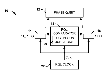
[0008] FIG. 1 illustrates an example of an RQL readout system.
[0009] FIG. 2 illustrates an example of an RQL readout circuit.
[0010] FIG. 3 illustrates an example of a timing diagram.
[0011] FIG. 4 illustrates an example of a method for reading a quantum state
of a phase qubit.
DETAILED DESCRIPTION
[0012] The present invention relates generally to quantum and classical
digital superconducting
circuits, and specifically to a reciprocal quantum logic (RQL) comparator for
qubit readout. An
RQL readout system can include an input stage on which a read pulse is
provided. The input
stage can include at least one input Josephson junction on which the read
pulse can propagate.
The read pulse can be provided, such as from an external RQL circuit, to
determine a quantum
state of a phase qubit. The RQL readout system can also include an output
stage configured to
propagate an output pulse in a first quantum state of the phase qubit in
response to the read pulse.
If the phase qubit is in the second quantum state, the output pulse is not
provided on the output
stage in response to the read pulse. The RQL readout system also includes an
RQL comparator
comprising a first Josephson junction and a second Josephson junction that are
coupled to the
phase qubit. The quantum state of the phase qubit can set a relative threshold
associated with
each of the first and second Josephson junctions. As an example, the phase
qubit can be
inductively coupled to the RQL comparator to provide a bias current flow in
either a first
direction or a second direction through the Josephson junctions depending on
the quantum state
of the phase qubit. Thus, one of the first and second Josephson junctions can
trigger in response
to the read pulse based on the bias current being either added to or
subtracted from the read pulse
based on the direction of current flow of the bias current through the first
and second Josephson
junctions, respectively, to either provide or not provide the output pulse on
the output stage.
3
CA 2941268 2018-01-24
100131 The RQL readout system also includes an RQL clock that provides RQL
clock signal to
each of the input stage, the output stage, and the RQL comparator. Because the
phase qubit can
be inductively coupled to the RQL comparator, the phase qubit can be
effectively isolated from
the RQL clock and the associated shunting resistors. As a result, the phase
qubit is decoupled
from potential noise sources to substantially prevent degradation of coherence
time of the phase
qubit. The RQL clock signal can affect the thresholds of the Josephson
junctions in the input
stage, the output stage, and the RQL comparator to facilitate triggering of
the Josephson
junctions, such that the read pulse can be provided at a first cycle (e.g.,
positive cycle) of the
RQL clock signal. During a second cycle (e.g., negative cycle) of the RQL
clock signal, a
negative pulse can be provided to reset the respective Josephson junctions,
thus allowing
subsequent readout of the quantum state of the phase qubit.
[0014] FIG. 1 illustrates an example of an RQL readout system 10. The RQL
readout system 10
can be implemented in a variety of quantum and classical computing
environments to read a
quantum state from a superconducting qubit 12. As an example, at least a
portion of the RQL
readout system 10 can be implemented on an integrated circuit (IC) in a
superconducting
environment. In the example of FIG. 1, the qubit 12 is configured as a phase
qubit. For
example, the phase qubit 12 can be arranged as a Josephson junction embedded
in a
superconducting loop (e.g., an inductor). Thus, the ''one" and "zero" quantum
states of the phase
qubit 12 can differ by the presence or absence of one flux quantum in the
inductor of the phase
qubit 12 (e.g., having a current difference of approximately 31.1A or less).
10015] The RQL readout system 10 also includes an input stage 14, an output
stage 16, and an
RQL comparator 18. The input stage 14 is configured to propagate a read pulse
RD_PLS that is
provided to read the quantum state of the phase qubit 12, such as during a
readout operation. As
an example, the read pulse RD_PLS can be generated from an external circuit,
such as the input
stage 14 can include at least one input Josephson junction that can
sequentially trigger to
propagate the read pulse RD_PLS. Similarly, the output stage 16 is configured
to propagate an
output pulse OUT that is generated in response to the read pulse RD_PLS in a
first quantum state
of the phase qubit 12. For example, the output stage 16 can include at least
one output Josephson
junction that can sequentially trigger to propagate the output pulse OUT to
indicate that the
4
CA 2941268 2018-01-24
phase qubit 12 is in the first quantum state. Conversely, if the phase qubit
12 is in the second
quantum state, no output pulse OUT is generated. Therefore, the output pulse
OUT is not
propagated at the output stage 16 in response to the read pulse RD PLS when
the phase qubit 12
is in the second quantum state.
[0016] The RQL comparator 18 is configured to determine the quantum state of
the phase qubit
12 in response to the read pulse RD PLS, and to generate the output pulse OUT
if the phase
qubit 12 is in the first quantum state. Therefore, the quantum state of the
phase qubit 12 can be
indicated to other quantum or classical circuits. For example, the output
pulse OUT can be
implemented for quantum error correction or a variety of other quantum or
classical processing
applications. In the example of FIG. 1, the phase qubit 12 is demonstrated as
coupled to the
RQL comparator 18 symmetrically, such that a bias current IQ can flow through
the RQL
comparator 18. The direction of the flow of the bias current IQ can be based
on the quantum
state of the phase qubit 12. For example, the phase qubit 12 can be
inductively coupled to the
RQL comparator 18, such that the bias current IQ can be magnetically induced
to flow through
the RQL comparator 18. As described herein, "inductive coupling" refers to
magnetic coupling
between respective inductors, such that a current flow through one inductor
induces a current
flow through the other inductor based on a magnetic field through a common
core of the
respective inductors.
[0017] In the example of FIG. 1, the RQL comparator 18 includes Josephson
junctions 20 that
can be arranged symmetrically with respect to the phase qubit 12. As an
example, the RQL
comparator 18 can include a first of the Josephson junctions 20 and a second
of the Josephson
junctions 20 through which the portions of the bias current IQ flow and which
are each coupled to
the output stage 16. The direction of the bias current IQ in the current loop
can thus
disproportionally affect a threshold of each of the first and second Josephson
junctions 20 to
selectively trigger one of the first and second Josephson junctions 20 in
response to the read
pulse RD PLS. As a result, in the first quantum state of the phase qubit 12,
the first Josephson
junction can trigger to provide the output pulse OUT. As an example, the bias
current IQ flowing
through the first of the Josephson junctions 20 can be added to the read pulse
RD PLS to exceed
the threshold of the first of the Josephson junctions 20, thus triggering the
first of the Josephson
CA 2941268 2018-01-24
junctions 20 to generate the output pulse OUT. Conversely, in the second
quantum state of the
phase qubit 12, the second Josephson junction can trigger to prevent the
output pulse OUT from
propagating on the output stage 16. As an example, the bias current IQ flowing
through the first
of the Josephson junctions 20 can be subtracted from the read pulse RD PLS to
not reach the
threshold of the first of the Josephson junctions 20 to not trigger the first
of the Josephson
junctions 20, but instead triggering the second of the Josephson junctions 20,
resulting in no
generation of the output pulse OUT.
[0018] The RQL readout system 10 also includes an RQL clock 22 that is
configured to generate
an RQL clock signal CLK. As an example, the RQL clock signal CLK can be a four
phase (e.g.,
quadrature) clock signal, such as having a very high frequency (e.g., tens of
gigahertz). In the
example of FIG. 1, the RQL clock signal CLK is demonstrated as being provided
to the input
stage 14, the output stage 16, and the RQL comparator 18. The read pulse
RD_PLS, when
combined with the RQL clock signal CLK, can exceed the thresholds of at least
a portion of the
input Josephson junctions in the input stage, the output Josephson junctions
in the output stage,
and the Josephson junctions 20 in the RQL comparator 18 to facilitate
triggering of the
respective Josephson junctions. For example, the read pulse can be provided at
a first cycle (e.g.,
positive cycle) of the RQL clock signal CLK, and during a second cycle (e.g.,
negative cycle) of
the RQL clock signal CLK, a negative pulse can be provided to reset the
respective Josephson
junctions. As an example, the RQL clock signal CLK can be provided to RQL
comparator 18 in
a common-mode connection, such that the Josephson junctions 20 are arranged
symmetrically
with respect to the RQL clock signal CLK. Therefore, based on the balanced
connection of the
RQL clock signal CLK in the input stage 14, the output stage 16, and the RQL
comparator 18,
the RQL clock signal CLK and associated shunt resistors do not imbalance the
bias current I.
Additionally, because of the inductive coupling of the phase qubit 12 to the
RQL comparator 18,
the RQL clock signal CLK is effectively isolated from the phase qubit 12.
[0019] The RQL readout system 10 therefore provides a manner for reading the
quantum state of
the phase qubit 12 in a very rapid manner with substantially mitigated
decoherence. Because the
RQL readout system 10 implements RQL-based quantum logic, the RQL readout
system 10 can
be configured to provide readout of the quantum state of the phase qubit 12 at
very rapid data
6
CA 2941268 2018-01-24
rates (e.g., reading the quantum state in less than one nanosecond) with
substantially minimal
losses and generated heat (e.g., operating at temperatures of approximately 20
mK without
causing local heating). Additionally, based on the balanced fabrication of the
RQL comparator
18 with respect to the arrangement of the Josephson junctions 20 and the
respective interaction
with the bias current IQ, the RQL readout system 10 can distinguish current
amplitude changes
of, for example, less than approximately 3 A, and can thus achieve a very high
sensitivity.
Furthermore, based on the isolation of the phase qubit 12 from the RQL clock
signal CLK and
based on the balanced arrangement of the RQL clock signal CLK, the RQL readout
system 10
can substantially mitigate decoherence of the quantum state of the phase qubit
12.
[0020] It is to be understood that the RQL readout system 10 is demonstrated
simplistically, such
that the RQL readout system 10 can include one or more circuit devices that
interconnect and/or
are included in the components of the RQL readout system 10. For example, as
described
herein, the term "coupled" can refer to electrical coupling through one or
more circuit devices
(e.g., an inductor) in the associated quantum circuit, such that current
and/or current pulses can
flow between coupled components through one or more inductors or other
devices. Therefore,
coupling between devices in the RQL readout system 10 can include coupling
through inductors
and/or other circuit devices.
[0021] FIG. 2 illustrates an example of an RQL readout circuit 50. The RQL
readout circuit 50
can correspond to the RQL readout system 10 in the example of FIG. 1.
Therefore, the RQL
readout circuit 50 can be implemented in a variety of quantum and classical
computing
environments to read a quantum state from a phase qubit 52. As an example, at
least a portion of
the RQL readout circuit 50 can be implemented on an IC in a superconducting
environment (e.g.,
at a very low temperature).
[0022] The RQL readout circuit 50 also includes an input stage 54, an output
stage 56, and an
RQL comparator 58. The input stage 54 is configured to propagate a read pulse
RD PLS that is
provided to read the quantum state of the phase qubit 52, such as during a
readout operation. As
an example, the read pulse RD PLS can be generated from an external circuit,
such as the input
stage 54 can include at least one input Josephson junction that can
sequentially trigger to
propagate the read pulse RD_PLS. The input stage 54 includes a set of
inductors through which
7
CA 2941268 2018-01-24
the read pulse RD_PLS is provided. In the example of FIG. 2, the input stage
54 includes a first
inductor LI, a second inductor L2, a third inductor L3, and a fourth inductor
L4. The input stage
54 also includes a first Josephson junction Ji that is coupled to the first
and second inductors L1
and L2 and to a low-voltage rail (e.g., ground), and includes a second
Josephson junction J2 that
is coupled to the third and fourth inductors L3 and L4 and to the low-voltage
rail.
[0023] The first and second Josephson junctions J1 and J2 are configured to
sequentially trigger
to propagate the read pulse RD PLS along the input stage 54 via the second,
third, and fourth
inductors L2, L3, and L4. In the example of FIG. 2, the RQL readout circuit 50
includes an RQL
clock 60 that is configured to generate the RQL clock signal CLK that is
provided to the input
stage 54 between the second and third inductors L2 and L3 via an inductive
coupling 61 (e.g., a
transformer) and an inductor Lci. The RQL clock signal CLK thus facilitates
triggering of the
first and second Josephson junctions J1 and J2. As an example, the read pulse
RD_PLS can be
provided substantially concurrently with a positive cycle of the RQL clock
signal CLK, such that
the first and second Josephson junctions J1 and J2 can have sufficient current
to trigger in
response to the read pulse RD_PLS. In the example of FIG. 2, the RQL clock
signal CLK is
shunted to ground via an inductor Lc2 and a resistor RI. In the arrangement of
the input stage 54,
the resistor R1 is also provided as a common shunting resistor for the first
and second Josephson
junctions Ji and J2. As a result, the inductor L3 can provide additional
inductive isolation of the
resistor R1 with respect to the phase qubit 52, such as to further mitigate
the effects of resistor
noise on the qubit coherence time of the phase qubit 52.
[0024] The RQL comparator 58 is configured to determine the quantum state of
the phase qubit
52 in response to the read pulse RD PLS, and to generate the output pulse OUT
if the phase
qubit 52 is in the first quantum state. In the example of FIG. 2, the inductor
LNI of the phase
qubit 52 is demonstrated as inductively coupled to an inductor LpQ, to induce
the current IQ
based on the quantum state of the phase qubit 52 through the inductor LpQ2 and
through a
transformer 62 that is arranged as an inductive common-mode choke (e.g., to
substantially
mitigate an inductance acting upon the current Iv). In the example of FIG. 2,
the current IQ is
demonstrated as currents IQI and IQ2 flowing in opposite directions. However,
it is to be
understood that the current IQ' and IQ2 correspond to the current IQ flowing
in opposite directions
8
CA 2941268 2018-01-24
depending on the quantum state of the phase qubit 52. For example, the current
IQ' can
correspond to the current IQ flowing in a first direction based on the phase
qubit 52 having a first
quantum state, and the current IQ2 can correspond to the current IQ flowing in
a second direction
based on the phase qubit 52 having a second quantum state. Therefore, the
currents IQ' and IQ2
are substantially equal in magnitude and direction based on the quantum state
of the phase
qubit 52.
[0025] The phase qubit 52 is inductively coupled to the RQL comparator 58 via
the inductor
Low, the transformer 62, an inductor L11 that is coupled to the input stage
54, and an inductor L01
that is coupled to the output stage 54. The RQL comparator 58 includes
Josephson junctions J3
and J4 that are each coupled to the inductor L11 at a node 64, and Josephson
junctions J5 and J6
that are each coupled to the inductor L01 at a node 66. The Josephson
junctions J4 and J5 are
coupled via inductors 1_,RQI and LRQ2, and the Josephson junctions J3 and 76
are coupled to
ground. Additionally, the RQL clock signal CLK is provided in a common-mode
manner
between the inductors I.Rco and LRQ2 via an inductive coupling 68 (e.g., a
transformer) and a pair
of inductors Lo and I.c4, with a shunt resistor R2 interconnecting the
inductors Lc3 and 44 to
ground. Therefore, the phase qubit 52 is symmetrically coupled to the RQL
comparator 58, and
the RQL comparator 58 is symmetric with respect to the circuit components
therein. Similar to
as described previously, the RQL clock signal CLK facilitates triggering of
the Josephson
junctions therein. As an example, the read pulse RD PLS can be provided
substantially
concurrently with a positive cycle of the RQL clock signal CLK, such that the
Josephson
junction J3 can propagate the read pulse RD_PLS to the Josephson junctions J5
and J6, and one of
the Josephson junctions J5 and J6 can have sufficient current to trigger in
response to the read
pulse RD PLS. In the example of FIG. 2, the resistor R2 is symmetrically
arranged with respect
to the phase qubit 52 as a common shunt resistor with respect to the Josephson
junctions J3, J4,
J5, and J6, as opposed to typical superconducting circuit applications in
which shunt resistors are
provided in parallel with each respective Josephson junction of the given
circuit. Accordingly,
the symmetrical common shunt arrangement of the resistor R2 substantially
mitigates the
presence of noise that could degrade a coherence time of the phase qubit 52.
9
CA 2941268 2018-01-24
[0026] As described previously, the direction of the flow of the bias current
IQ can be based on
the quantum state of the phase qubit 52, and thus flows through the inductor
L01 and into the
node 66 as the current IQI, or flows out from the node 66 and through inductor
L01 as the current
IQ2. In the example of FIG. 2, the current IQi is demonstrated as splitting at
the node 66, with a
first portion of the current IQ I (demonstrated as a current 1,51) flowing
through the Josephson
junction J5 to the inductor LRQ2 and a second portion of the current IQ]
(demonstrated as a current
'Jo') flowing through the Josephson junction J6 to ground. Similarly, the
current IQ2 is
demonstrated as joining at the node 66, with a first portion of the current
1Q2 (demonstrated as a
current 1,52) flowing through the Josephson junction J5 to the node 66 and a
second portion of the
current IQ2 (demonstrated as a current 1_162) flowing through the Josephson
junction J6 to the node
66 from ground. Therefore, currents IJ51 and 1.161 correspond to the current
IQ', and thus the first
quantum state of the phase qubit 52, and the currents Ij52 and 1j62 correspond
to the current IQ2,
and thus the second quantum state of the phase qubit 52. Accordingly, the
currents IJ51 and Ij61
and the currents 1,152 and IJ62 change the relative threshold of the Josephson
junctions J5 and J6
with respect to the read pulse RD_PLS.
[0027] During a read operation, the read pulse RD_PLS propagates through the
input stage 54
(e.g., through the inductors LI, L2, L3, and L4 via the Josephson junctions J1
and J2) and through
the inductor L11 to trigger the Josephson junction J3. The read pulse RD PLS
thus gets
propagated through inductors LRQ1 and LRQ2 to the Josephson junctions J5 and
J6. Thus, the bias
current IQ is either added to or subtracted from the read pulse RD_PLS with
respect to Josephson
junctions Js and J6 based on the quantum state of the phase qubit 52.
[0028] For example, in the first quantum state of the phase qubit 52, the
current IQ! flows into
the node 66, and thus the current IJ51 flows from the node 66 through the
Josephson junction J5
and the current IJ61 flows from the node 66 through the Josephson junction J6.
Because the
current lis flows oppositely with respect to the read pulse RD_PLS propagated
from the
Josephson junction J3 and through the inductors LRQ1 and LRQ2, the current
IJ51 is subtracted from
the read pulse RD_PLS (e.g., increases the threshold of the Josephson junction
J5). Thus,
Josephson junction J5 does not trigger in the first quantum state of the phase
qubit 52. However,
because the current IJ6l flows in the same direction as the read pulse RD_PLS
propagated from
CA 2941268 2018-01-24
the Josephson junction J3 and through the inductors LRQJ and LRQ2, the current
IJ61 is added to the
read pulse RD_PLS (e.g., decreases the threshold of the Josephson junction
J6). Thus, Josephson
junction J6 triggers in the first quantum state of the phase qubit 52.
100291 As another example, in the second quantum state of the phase qubit 52,
the current 1Q2
flows from the node 66, and thus the current 1.152 flows into the node 66
through the Josephson
junction J5 and the current IJ62 flows into the node 66 through the Josephson
junction J6. Because
the current 1J52 flows in the same direction as the read pulse RD_PLS
propagated from the
Josephson junction J3 and through the inductors LRQ1 and LRQ2, the current
1_152 is added to the
read pulse RD_PLS (e.g., decreases the threshold of the Josephson junction
J5). Thus, Josephson
junction J5 triggers in the second quantum state of the phase qubit 52.
However, because the
current 1.162 flows in the opposite direction as the read pulse RD_PLS
propagated from the
Josephson junction J3 and through the inductors LRQ1 and LRQ2, the current
Ij62 is subtracted from
the read pulse RD_PLS (e.g., increases the threshold of the Josephson junction
J6). Thus,
Josephson junction J6 does not trigger in the second quantum state of the
phase qubit 52.
100301 The output stage 56 is configured to propagate the output pulse OUT
that is generated in
response to the triggering of the Josephson junction J6, and thus in the first
quantum state of the
phase qubit 52. The output stage 56 is demonstrated in the example of FIG. 2
as being arranged
substantially similar (e.g., symmetrical) with respect to the input stage 54.
In the example of
FIG. 2, the output stage 56 includes a set of inductors through which the
output pulse OUT
propagates from the Josephson junction J6 and through the inductor L01. In the
example of FIG.
2, the output stage 56 includes a first inductor L5, a second inductor L6, a
third inductor L7, and a
fourth inductor Lg. The output stage 56 also includes a first Josephson
junction J7 that is coupled
to the third and fourth inductors L7 and Lg and to ground, and includes a
second Josephson
junction J8 that is coupled to the first and second inductors L5 and L6 and to
ground. The first
and second Josephson junctions J7 and J8 are configured to sequentially
trigger to propagate the
output pulse OUT along the output stage 56 via the second, third, and fourth
inductors L6, 1-7,
and Lg. In the example of FIG. 2, the RQL clock signal CLK is provided to the
output stage 56
between the second and third inductors L6 and L7 via an inductive coupling 70
(e.g., a
transformer) and an inductor Lc5, and is shunted to ground via an inductor LC6
and a resistor R3.
11
CA 2941268 2018-01-24
In the arrangement of the output stage 56, the resistor R3 is also provided as
a common shunting
resistor for the first and second Josephson junctions J7 and J8. As a result,
the inductor L6 can
provide additional inductive isolation of the resistor R3 with respect to the
phase qubit 52, such as
to further mitigate the effects of resistor noise on the qubit coherence time
of the phase qubit 52.
[0031] The RQL clock signal CLK thus facilitates triggering of the first and
second Josephson
junctions J7 and Jg. Accordingly, in response to the triggering of the
Josephson junction J6 in
response to the read pulse RD_PLS in the first quantum state of the phase
qubit 52, the output
pulse OUT is provided at the output stage 56 to indicate the first quantum
state of the phase qubit
52. Conversely, in response to the triggering of the Josephson junction J5
instead of the
Josephson junction J6 in response to the read pulse RD_PLS in the second
quantum state of the
phase qubit 52, the output pulse OUT is not provided at the output stage 56 to
indicate the
second quantum state of the phase qubit 52.
[0032] It is to be understood that the RQL readout circuit 50 is not limited
to the example of
FIG. 2. As an example, the input stage 54 and the output stage 56 are not
limited to as
demonstrated in the example of FIG. 2, but can include additional circuit
components, such as
one or more additional Josephson junctions and/or one or more additional
inductors.
Additionally, the readout operation described herein is not limited to readout
of a phase qubit 52,
but a variety of other qubits or circuit devices having logic or quantum
states that are based on a
current flow direction can be implemented in the RQL readout circuit 50.
Accordingly, the RQL
readout circuit 50 can be configured in a variety of ways.
[0033] FIG. 3 illustrates an example of a timing diagram 100. The timing
diagram 100 can
correspond to the timing of the RQL readout circuit 50. Therefore, reference
is to be made to the
example of FIG. 2 in the following description of the example of FIG. 3. The
timing diagram
100 demonstrates the current IQI, such that a positive magnitude of the
current IQI demonstrates
that the current IQ is provided as the current IQI in the first quantum state
of the phase qubit 52
and a negative magnitude of the current IQI demonstrates that the current IQ
is provided as the
current IQ2 in the second quantum state of the phase qubit 52. The timing
diagram 100 also
demonstrates the read pulse RD_PLS, the current 451, the current Iml, and the
output pulse OUT.
The current IJ51 is demonstrated as having a negative magnitude when the
current IQ is provided
12
CA 2941268 2018-01-24
as the current IQ2 in the second quantum state, and is demonstrated as having
a positive
magnitude to correspond to the current 1152 when the current IQ is provided as
the current IQ' in
the first quantum state. Similarly, the current Ija I is likewise demonstrated
as having a negative
magnitude when the current IQ is provided as the current 1Q1 in the second
quantum state, and is
demonstrated as having a positive magnitude to correspond to the current IJ62
when the current IQ
is provided as the current IQ2 in the first quantum state.
[0034] At a time To, the current IQI is negative, such that the phase qubit 52
is in the second
quantum state. The read pulse RD_PLS is provided at the input stage 54, such
as concurrently
with a positive cycle of the RQL clock signal CLK. The current 1,151 is
negative at the time To,
and thus is added to the read pulse RD_PLS with respect to the Josephson
junction J5. The
current 1J61 is also negative, and thus is subtracted from the read pulse
RD_PLS with respect to
the Josephson junction J6. Therefore, the Josephson junction J5 triggers, and
the Josephson
junction J6 does not trigger. As a result, the output pulse OUT is not
generated and propagated
along the output stage 56. Accordingly, the output stage 56 indicates that the
phase qubit 52 is in
the second quantum state. At a time T1, the read pulse RD_PLS is provided as a
negative pulse,
such as substantially concurrently with a negative cycle of the RQL clock
signal CLK, to reset
the Josephson junctions of the RQL readout circuit 50. At a time T2, the read
pulse RD PLS is
provided again, resulting in an indication of the phase qubit 52 being in the
second quantum state
again, similar to as described previously. At a time T3, the read pulse RD_PLS
is again provided
as a negative pulse to reset the Josephson junctions of the RQL readout
circuit 50.
[0035] At a time Ta, the current IQ1 is positive, such that the phase qubit 52
is in the first
quantum state. The read pulse RD_PLS is provided at the input stage 54, the
current 1j51 is
positive, and thus is subtracted from the read pulse RD_PLS with respect to
the Josephson
junction J5. The current Ij61 is likewise positive, and thus is added to the
read pulse RD_PLS
with respect to the Josephson junction J6. Therefore, the Josephson junction
J5 does not trigger,
and the Josephson junction J6 triggers. As a result, the output pulse OUT is
generated and
propagates along the output stage 56. Accordingly, the output stage 56
indicates that the phase
qubit 52 is in the first quantum state. At a time T5, the read pulse RD_PLS is
provided as a
negative pulse to reset the Josephson junctions of the RQL readout circuit 50.
At a time T6, the
13
CA 2941268 2018-01-24
read pulse RD_PLS is provided again, resulting in an indication of the phase
qubit 52 being in
the first quantum state again, similar to as described previously. At a time
T7, the read pulse
RD PLS is again provided as a negative pulse to reset the Josephson junctions
of the RQL
readout circuit 50.
[0036] In view of the foregoing structural and functional features described
above, a
methodology in accordance with various aspects of the present invention will
be better
appreciated with reference to FIG. 4. While, for purposes of simplicity of
explanation, the
methodology of FIG. 4 is shown and described as executing serially, it is to
be understood and
appreciated that the present invention is not limited by the illustrated
order, as some aspects
could, in accordance with the present invention, occur in different orders
and/or concurrently
with other aspects from that shown and described herein. Moreover, not all
illustrated features
may be required to implement a methodology in accordance with an aspect of the
present
invention.
[0037] FIG. 4 illustrates an example of a method 150 for reading a quantum
state of a phase
qubit (e.g., the phase qubit 12). At 152, a bias current (e.g., the bias
current Io) is provided
through a first Josephson junction (e.g., the Josephson junction J6) and a
second Josephson
junction (e.g., the Josephson junction J5) in a first direction (e.g., the
bias current TO in a first
quantum state of the phase qubit and in a second direction (e.g., the bias
current 10 in a second
quantum state of the phase qubit. At 154, a read pulse (e.g., the read pulse
RD_PLS) is applied
at a first cycle of an RQL clock signal (e.g., the RQL clock signal CLK), the
read pulse being
propagated on an input stage (e.g., the input stage 14) to the first and
second Josephson
junctions. At 156, the phase qubit is determined to be in the first quantum
state based on
receiving an output pulse (e.g., the output pulse OUT) at an output stage
(e.g., the output
stage 16) in response to the read pulse the first Josephson junction
triggering based on the bias
current being provided in the first direction and the read pulse, or in the
second quantum state
based on not receiving output pulse at the output stage in response to the
second Josephson
junction triggering based on the bias current being provided in the second
direction and the read
pulse.
14
CA 2941268 2018-01-24
100381 What have been described above are examples of the invention. It is, of
course, not
possible to describe every conceivable combination of components or
methodologies for
purposes of describing the invention, but one of ordinary skill in the art
will recognize that many
further combinations and permutations of the invention are possible.
Accordingly, the invention
is intended to embrace all such alterations, modifications, and variations
that fall within the
scope of this application, including the appended claims.
CA 2941268 2018-01-24