Note: Descriptions are shown in the official language in which they were submitted.
CA 02941282 2016-09-08
Agent's Ref: 52868-93
12G-SDI Switcher with Integrated Processing of Quad-link 3G-SDI
PRIORITY CLAIM
[1] This application claims priority to U.S. Provisional Patent Application
Serial No.
62/215,693, filed on September 8, 2015.
FIELD
[2] The present application relates to the processing and routing of ultra-
high
definition (UHD) signals that are transported using quad-link 3G-SDI and/or
12G-SDI.
BACKGROUND
131 In the broadcast audio/video environment, video and audio signals
are typically
represented in a digital manner, and different transports may be used to move
these signals
between different equipment. One such transport is Serial Digital Interface
(SDI), which is
specified by the Society of Motion Pictures and Television Engineers (SMPTE)
and the
International Telecommunications Union (ITU). This signal transport carries
audio and video
signals in a serial bit stream between devices over a variety of media,
including coaxial cable or
fiber optic cable.
[4] The SDI standards can represent a wide variety of video standards,
including
National Television System Committee (NTSC), Phase Alternating Line (PAL),
High Definition
(HD) Television (1080i, 720p, 1080p), or Ultra-High Definition (UHD)
Television (2160p).
Depending upon the video standard being carried, the data rate of an SDI
transport may vary
among a number of pre-defined rates, ranging from 270 megabits per second
(270Mbps) up to 12
gigabits per second (12Gbps).
[5] As new standards are defined, the technology to fully implement these
standards
sometimes trails. In these situations, bridge technologies may be defined. For
example, when
High Definition Serial Data Interface (HD-SDI) evolved from 1.5Gbps transport
to 3Gbps
transport, a bridge standard was defined that allows a 3Gbps payload to be
carried over two
1.5Gbps physical links. This is known as a "dual-link".
1
CA 02941282 2016-09-08
Agent's Ref: 52868-93
[6] Similarly, when 12Gbps Serial Digital Interface (12G-SDI) Ultra-High
Definition
standards were defined, a bridge standard was also defined that allows a
12Gbps payload to be
carried over four 3Gbps physical links. This is known as "quad-link 3G-SDI".
SUMMARY
[7] It some installations it may be necessary to switch between 12G-SDI,
which is a
12Gbps interface on a single link, and quad-link 3G-SDI, which uses four 3Gbps
physical links.
[8] In one embodiment, an apparatus, such as a routing switcher, is
provided that
routes 12G-SDI signals between input ports and output ports. However, the
apparatus also has
the capability to receive quad-link 3G-SDI signals at its input ports and
internally convert from
quad-link 3G-SDI to 12G-SDI. The apparatus also has the capability to
internally convert a 12G-
SDI signal into a quad-link 3G-SDI signal for output on its output ports. In
some embodiments,
additional processing, such as link healing and deskewing of incoming quad-
link 3G-SDI
signals, may be performed.
[9] According to one embodiment, there is provided an apparatus having a
plurality
of input ports and a plurality of output ports. The apparatus further includes
a switch matrix to
route 12G-SDI signals between the input ports and the output ports. A first
convertor may be
interposed between the input ports and the switch matrix. The first convertor
converts a quad-
link 3G-SDI signal received at four of the input ports into a 12G-SDI signal
destined for the
switch matrix. A second convertor may be interposed between the switch matrix
and the output
ports. The second convertor converts a 12G-SDI signal received from the switch
matrix into a
quad-link 3G-SDI signal destined for four of the output ports. In some
embodiments, the
apparatus may be a routing switcher or a production switcher or a master
control switcher.
[10] In some embodiments, the apparatus includes a link healer interposed
between the
input ports and the switch matrix. The link healer performs interpolation to
compute missing
pixel values when one or two or three links of the quad-link 3G-SDI signal
received at the input
ports have failed. The interpolation uses pixel values received on one or more
links of the quad-
link 3G-SDI signal that have not failed. The interpolation may be bilinear
interpolation. For
2
CA 02941282 2016-09-08
Agent's Ref: 52868-93
= example, if a single link fails, then interpolation may be performed
using pixel values from one,
some, or all of the other three links, which have not failed.
[11] In some embodiments, the apparatus includes a deskewer interposed
between the
input ports and the switch matrix. The deskewer removes skew from the quad-
link 3G-SDI
signal received at the input ports.
[12] In some embodiments, a sampler is interposed between the input ports
and the
switch matrix. The sampler performs at least one of upsampling and
downsampling of at least
one signal received at the input ports. In one embodiment, the sampler
performs trunking by: (i)
downsampling each of a plurality of signals received at the input ports to
produce a plurality of
downsampled signals; and (ii) combining the downsampled signals into a 12G-SDI
signal to be
sent to the switch matrix. In one embodment, the sampler is to: (i) generate
four 3Gbps signals
by: for each input port of four of the input ports, downsampling a 12G-SDI
signal received at the
input port into a 3Gbps signal; and (ii) combine the four 3Gbps signals into a
12G-SDI signal to
be sent to the switch matrix.
[13] In some embodiments, a sampler is also or instead interposed between
the switch
matrix and the output ports. The sampler performs at least one of upsampling
and downsampling
of at least one signal received from the switch matrix. In one embodiment, the
sampler performs
trunking by: (i) downsampling each of a plurality of 12G-SDI signals received
from the switch
matrix to produce a plurality of downsampled signals; and (ii) combining the
downsampled
signals into an output signal to be sent out one of the output ports. In one
embodiment, the
sampler is to: (i) downsample each one of three 12G-SDI signals received from
the switch matrix
to generate three 3Gbps signals; and (ii) incorporate the three 3Gbps signals
into a 10Gbps
Ethernet signal to be sent out of an output port.
[14] In some embodiments, the first convertor is to convert from quadrant
mapping
quad-link 3G-SDI to 12G-SDI and/or from two sample interleave mapping quad-
link 3G-SDI to
12G-SDI. In some embodiments, the second convertor is to convert from 12G-SDI
to quadrant
mapping quad-link 3G-SDI and/or from 12G-SDI to two sample interleave mapping
quad-link
3G-SDI.
3
CA 02941282 2016-09-08
=
Agent's Ref: 52868-93
= [15] In another embodiment, there is provided a method in a
routing apparatus that
includes receiving a quad-link 3G-SDI signal at four input ports of the
apparatus. The method
further includes converting the quad-link 3G-SDI signal into a corresponding
12G-SDI signal
within the apparatus, and routing the corresponding 12G-SDI signal through a
switch matrix in
the apparatus.
[16] In another embodiment, there is provided a method in a routing
apparatus that
includes converting, within the apparatus, a 12G-SDI signal from a switch
matrix into a
corresponding quad-link 3G-SDI signal, and then forwarding the corresponding
quad-link 3G-
SDI signal to four output ports of the apparatus.
[17] In another embodiment, there is provided a method that includes
receiving a
quad-link 3G-SDI signal at four input ports of a routing apparatus. The quad-
link 3G-SDI signal
is converted into a corresponding 12G-SDI signal within the apparatus. The
corresponding 12G-
SDI signal is routed through a switch matrix of the apparatus. A 12G-SDI
signal from the switch
matrix (not necessarily the corresponding 12G-SDI signal) may also be
converted into a
corresponding quad-link 3G-SDI signal. The corresponding quad-link 3G-SDI
signal may be
routed to four output ports of the apparatus.
[18] In some embodiments, a method further includes performing
interpolation in the
apparatus to compute missing pixel values when one or two or three links of
the quad-link 3G-
SDI signal received at the input ports have failed. The interpolation uses
pixel values received on
one or more links of the quad-link 3G-SDI signal that have not failed.
[19] In some embodiments, a method further includes removing skew from the
quad-
link 3G-SDI signal received at the input ports.
[20] In some embodiments, a method further includes performing at least one
of
upsampling and downsampling of at least one signal received at the input
ports. The method may
further include performing trunlcing in the apparatus by: (i) downsampling
each of a plurality of
signals received at the input ports to produce a plurality of downsampled
signals; and (ii)
combining the downsampled signals into a 12G-SDI signal that is sent to the
switch matrix. The
method may further include (i) generating four 3Gbps signals by: for each
input port of four of
4
81798574
the input ports, downsampling a 12G-SDI signal received at the input port into
a 3Gbps signal; and
(ii) combining the four 3Gbps signals into a 12G-SDI signal that is sent to
the switch matrix.
[21] In some embodiments, a method further includes performing at least one
of
upsampling and downsampling of at least one signal received from the switch
matrix. The method
may further include performing trunking in the apparatus by: (i) downsampling
each of a plurality of
12G-SDI signals received from the switch matrix to produce a plurality of
downsampled signals;
and (ii) combining the downsampled signals into an output signal that is sent
out one of the output
ports. The method may further include: (i) downsampling each one of three 12G-
SDI signals
received from the switch matrix to generate three 3Gbps signals; and (ii)
incorporating the three
3Gbps signals into a 10Gbps Ethernet signal that is sent out of an output
port.
[22] In some embodiments, the quad-link 3G-SDI signal received at four of
the input ports
is quadrant mapping quad-link 3G-SDI or two sample interleave mapping quad-
link 3G-SDI. The
converting the 12G-SDI signal from the switch matrix into the corresponding
quad-link 3G-SDI
signal may include converting the 12G-SDI signal from the switch matrix into a
quadrant mapping
quad-link 3G-SDI signal or a two sample interleave mapping quad-link 3G-SDI
signal.
[22a] According to another embodiment of the present invention, there is
provided an
apparatus comprising: a plurality of input ports and a plurality of output
ports; a switch matrix to
route 12 Gigabits per second Serial Digital Interface (12G-SDI) signals
between the input ports and
the output ports; a first convertor interposed between the input ports and the
switch matrix, the first
convertor to convert a quad-link 3 Gigabits per second Serial Digital
Interface (3G-SDI) signal
received at four of the input ports into a 12G-SDI signal destined for the
switch matrix; a second
convertor interposed between the switch matrix and the output ports, the
second convertor to convert
a 12G-SDI signal received from the switch matrix into a quad-link 3G-SDI
signal destined for four
of the output ports; a link healer interposed between the input ports and the
switch matrix, the link
healer to perform interpolation to compute missing pixel values when one or
two or three links of
the quad-link 3G-SDI signal received at the input ports have failed, the
interpolation using pixel
values received on one or more links of the quad-link 3G-SDI signal that have
not failed.
[22b] According to yet another embodiment of the present invention, there
is provided a
method comprising: receiving a quad-link 3 Gigabits per second Serial Digital
Interface (3G-SDI)
Date Recue/Date Received 2022-03-24
81798574
signal at four input ports of a routing apparatus; converting the quad-link 3G-
SDI signal into a
corresponding 12G-SDI signal within the apparatus; routing the corresponding
12G-SDI signal
through a switch matrix; converting a 12G-SDI signal from the switch matrix
into a corresponding
quad-link 3G-SDI signal; and forwarding the corresponding quad-link 3G-SDI
signal to four output
ports of the apparatus; the method further comprising performing interpolation
in the apparatus to
compute missing pixel values when one or two or three links of the quad-link
3G-SDI signal
received at the input ports have failed, the interpolation using pixel values
received on one or more
links of the quad-link 3G-SDI signal that have not failed.
[23] Specific aspects and features will become apparent to those of
ordinarily skill in the
art upon review of the following description.
BRIEF DESCRIPTION OF THE DRAWINGS
[24] Embodiments will be described, by way of example only, with reference
to the
accompanying figures wherein:
[25] FIG. 1 is a schematic block diagram illustrating gearboxes converting
between quad-
link 3G-SDI and 12G-SDI;
[26] FIG. 2 is a simplified schematic block diagram of a 3G-SDI routing
switcher;
[27] FIG. 3 is a simplified schematic block diagram of a 12G-SDI routing
switcher;
5a
Date Recue/Date Received 2022-03-24
CA 02941282 2016-09-08
Agent's Ref: 52868-93
= [28] FIG. 4 illustrates one way in which a UHD image may be
partitioned in order to
transmit the image pixels using quad-link 3G-SDI;
[29] FIG. 5 illustrates another way in which a UHD image may be partitioned
in order
to transmit the image pixels using quad-link 3G-SDI;
[30] FIG. 6 illustrates two adjacent image tiles in the situation in which
the fourth
quad-link 3G-SDI signal link has failed;
[31] FIG 7 illustrates image tiles in which neighbouring pixels are used to
interpolate
pixel values for missing pixels;
[32] FIG. 8 illustrates a 42 x 42 routing switcher in which 7 FPGAs each
serve as the
input and output processors;
[33] FIG. 9 illustrates an apparatus having a switch matrix to route 12G-
SDI data
signals between input ports and the output ports; and
[34] FIG. 10 is a flow chart illustrating a method of switching.
[35] Like reference numerals are used in different figures to denote
similar elements.
DETAILED DESCRIPTION
[36] For illustrative purposes, specific example embodiments will now be
explained in
greater detail below in conjunction with the figures.
[37] The embodiments set forth herein represent information sufficient to
practice the
claimed subject matter. Upon reading the following description in light of the
accompanying
figures, those of sufficient skill will understand the concepts of the claimed
subject matter and
will recognize applications of these concepts not particularly addressed
herein. It should be
understood that these concepts and applications fall within the scope of the
disclosure and the
accompanying claims.
[38] As mentioned above, when 12Gbps Serial Digital Interface (12G-SDI)
Ultra-High
Definition (UHD) standards were defined, the bridge standard "quad-link 3G-
SDI" was also
6
CA 02941282 2016-09-08
Agent's Ref: 52868-93
defined, which allows a 12Gbps payload to be carried over four 3Gbps physical
links. What this
means is that some equipment exists that implements the 12G-SDI interface,
i.e., transmitting the
UHD data over a single SDI link at 12Gbps, whereas other equipment exists that
implements the
quad-link 3G-SDI interface, i.e., splitting the 12Gbps payload into four 3Gbps
payloads and
transmitting the four 3Gbps payloads in parallel over four 3Gbps physical
links. For 12G-SDI,
only a single cable is required to carry the complete signal payload. However,
implementing
12G-SDI may be more technically challenging and more costly per physical link,
and signals
may not be carried as far on the 12G-SDI link compared to a quad-link 3G-SDI
interface (e.g. a
12G-SDI signal may only be carried approximately one half the distance of a 3G-
SDI signal).
Quad-link 3G-SDI may be less expensive per link, simpler to implement, and
have
approximately double the cable reach of 12G-SDI. The downfall is that quad-
link 3G-SDI
requires 4 cables to be run for each signal payload. For this reason, quad-
link 3G-SDI may have
a higher overall cost of implementation. Thus, in light of these different
trade-offs, some
equipment implements the 12G-SDI interface, while other equipment instead
implements the
quad-link 3G-SDI interface.
[39] In order to connect equipment that uses 12G-SDI with equipment that
uses quad-
link 3G-SDI, a device may be placed in between the equipment to convert one
interface to the
other. Such a device is sometimes called a "gearbox". A gearbox may convert
quad-link 3G-SDI
to 12G-SDI, 12G-SDI to quad-link 3G-SDI, or perform both functions.
[40] FIG. 1 is a schematic block diagram illustrating gearboxes converting
between
quad-link 3G-SDI and 12G-SDI. Gearbox 102 receives (over four links) quad-link
3G-SDI from
Equipment A, as shown at 104, and the gearbox 102 converts this to 12G-SDI,
which is then sent
(over one link) to Equipment B, as shown at 106. Conversely, gearbox 202
receives (on a single
link) 12G-SDI from Equipment C, as shown at 204, and the gearbox 202 converts
this to quad-
link 3G-SDI, which is then sent (over four links) to Equipment D, as shown at
206.
[41] An installation may require multiple gearboxes (as in FIG. 1) to adapt
multiple
pieces of equipment to interface with each other. In addition, the
configuration may become
awkward for a user when flexible signal routing and patching is required. For
example, if
multiple equipment with differing interfaces are connected to an SDI routing
switcher,
7
CA 02941282 2016-09-08
Agent's Ref: 52868-93
= mechanisms may need to be put into place to allow any source (either 12G-
SDI or Quad-link 3G-
SDI) to be connected to any destination (either 12G-SDI or Quad-link 3G-SDI).
[42] Furthermore, some routing switchers do not support 12G-SDI. therefore
necessitating all 12G-SDI signals to be processed by a gearbox to present as
quad-link 3G-SDI
for all sources and destinations. For example, FIG. 2 is a simplified
schematic block diagram of
an example 3G-SDI routing switcher 250 routing SDI signals between different
equipment. The
routing switcher 250 has an 1/0 region 252 and a switching matrix region 254,
the boundary of
which is shown by stippled line 256. In actual implementation, there may be no
actual physical
boundary or transition between these two regions. The I/O region 252 hosts the
user interface(s)
and any related processing. In particular, in the FIG. 2 embodiment, the I/0
region 252 includes
eight input ports 258 and eight output ports 260 to which the user may connect
cables. The
routing switcher 250 can route an incoming signal arriving at any of the input
ports 258 to any of
the output ports 260. A panel 262 having a user interface is also illustrated,
which consists of
user inputs, such as buttons (not shown), that allow a user to select which
input port is to switch
to which output port. The I/O region 252 may include some signal processing
equipment (not
shown), such as an equalizer connected to each of the input ports 258, a
driver connected to each
of the output ports 260, and clock re-timers.
[43] The switching matrix region 254 includes a switch matrix 264, which is
an
integrated circuit chip that performs the actual switching of signals between
the input ports 258
and the output ports 260. The switch matrix 264 is controlled by a
microcontroller 266, which
receives instructions from user inputs at the panel 262, as well as from an
external computer 268.
The routing switcher 250 may also include other components necessary or useful
for its
operation, such as a power supply 270 and a fan 272.
[44] Note that only one switch matrix 264 integrated circuit chip is
illustrated in FIG.
2. However, it will be appreciated that more generally the switching matrix
region 254 could
instead have multiple integrated circuit chips to implement the switching
between the input and
output ports. There could even be multiple switching matrix regions in some
implementations
(e.g. located on separate circuit boards). Also, only a single panel 262 is
illustrated in FIG. 2, but
more generally there may be multiple panels, and the panel(s) may be part of
the same chassis as
8
CA 02941282 2016-09-08
Agent's Ref: 52868-93
s the rest of the routing switcher 250, or an external apparatus. Also, the
exact location of the
power supply 270 and fan 272 is implementation specific and is shown just as
an example. More
generally, there may be one or more power supplies and one or more fans, with
the location of
each dependent upon the implementation. The power supply (or power supplies)
may even he
external to the routing switcher 250. As another example, the microcontroller
266 may be in
another location separate from the system in which the switch matrix is
located. Also, more
generally, the number of input and output ports may be much larger. In short,
the FIG. 2 diagram
is simplified for ease of explanation. In actual implementation, the exact
size and specific
structure, as well as the specific location of components, would depend upon
the implementation.
[45] The example routing switcher 250 of FIG. 2 is an 8 x 8 router, as it
can receive up
to 8 input signals and switch to up to 8 outputs. It operates at 3Gbps and
therefore can handle
switching 3G-SDI signals. If a piece of equipment connected to the routing
switcher 250
implements 12G-SDI, then an external gearbox is required. In the FIG. 2
illustration, four pieces
of equipment are shown: Equipment E, F, G, and H. Equipment F and G both
implement the
quad-link 3G-SDI interface (i.e. send/receive quad-link 3G-SDI signals),
whereas equipment E
and H both implement the 12G-SDI interface (i.e. send/receive 12G-SDI
signals). Gearbox 274
is therefore interposed between Equipment E and the routing switcher 250 to
convert the 12G-
SDI signal arriving from Equipment E into quad-link 3G-SDI, and gearbox 276 is
interposed
between Equipment H and the routing switcher 250 to convert quad-link 3G-SDI
arriving from
the routing switcher 250 into 12G-SDI.
[46] In operation, a user utilizes the computer 268 to configure the
routing switcher
250. For example, the user may utilize the computer 268 to configure the
routing switcher 250 so
that the four input ports receiving the quad-link 3G-SDI switch together.
During operation of the
routing switcher 250, the user may use the panel 252 to control the switching
of signals between
the input and output ports in order to route signals from Equipment E and F
(sources) to
Equipment G and H (destinations).
[47] Note that if the routing switcher 250 is being used to route UHD
signals, as
illustrated, then the routing switcher 250 requires all sources and
destinations to occupy 4 ports
each. Furthermore, when a 12G-SDI source is routed to a 12G-SDI destination,
it must be passed
9
CA 02941282 2016-09-08
Agent's Ref: 52868-93
= through two external gearboxes (one upstream of the routing switcher 250,
and one downstream
of the routing switcher 250). For example, if 12G-SDI Equipment E is routed to
12G-SDI
Equipment H, it must be routed through two external gearbox devices 274 and
276, which is
added complexity.
[48] Using a 3Gbps routing switcher, such as routing switcher 250 in FIG.
2, to route
UHD (12Gbps) signals is sometimes called "standardizing on quad-link 3G-SDI".
A possible
benefit of such an implementation is that the routing switcher only has to
operate at 3Gbps,
which may be easier to design and achieve compared to routing at 12Gbps.
However,
standardizing on quad-link 3G-SDI has possible drawbacks: notably, the
requirement that each
piece of UHD equipment must occupy four ports, and if a particular piece of
equipment
implements 12G-SDI, then an external gearbox is required to convert between
12G-SDI and
quad-link 3G-SDI. Standardizing on quad-link 3G-SDI for the routing switcher
may also
introduce a further challenge to a user. In particular, a broadcast facility
may provide manual
patch panels for signals, which allow signal paths to be manually patched by
connecting patch
cables between sources and destinations. This may be done to allow more
flexible configurations
or to provide a passive emergency bypass path, should active equipment
(including the routing
switcher) fail. In quad-link 3G-SDI implementations, the user must manually
patch 4
independent cables, which may take more time and may increase the likelihood
of error
compared to patching one cable carrying 12G-SDI. Also, when the routing
switcher is to switch
a quad-link 3G-SDI signal, it must be properly configured and instructed to
switch all four links
in the correct manner to keep the source links correlated with the four links
of the desired
destination. For example, with reference to FIG. 2, the routing switcher 250
does not know that
the four inputs arriving from gearbox 274 are related (i.e. a quad-link,
rather than 4 independent
3Gbps signals). The user must use the computer 268 to configure the routing
switcher 250 to
switch these four links at the same time in the correct manner.
[49] FIG. 3 is a simplified schematic block diagram of an example 12G-SDI
routing
switcher 350. It is a native 12G capable routing switcher; i.e., the signals
it routes internally
within the routing switcher are 12Gbps. The routing switcher 350 has an I/O
region 352 and a
switching matrix region 354, the boundary of which is shown by stippled line
356. In actual
CA 02941282 2016-09-08
=
Agent's Ref: 52868-93
= implementation, there may be no actual physical boundary or transition
between these two
regions. The I/O region 352 includes twelve input ports 358 and twelve output
ports 360 to
which the user may connect cables. The routing switcher 350 can route an
incoming signal
arriving at any of the input ports 358 to any of the output ports 360. A panel
362 is also
illustrated having a user interface consisting of user inputs, such as buttons
(not shown), that
allow a user to select which input port is to switch to which output port. The
I/O region 352
further includes an input processor 390, to which the input ports 358 are
connected, and an
output processor 392, to which the output ports 360 are connected. The input
processor 390 and
output processor 392 are constructed of one or more signal processing devices
that are
configured to perform the operations described herein. The input processor 390
and output
processor 392 may be implemented using dedicated integrated circuitry, such as
an ASIC or
FPGA, or the input processor 390 and output processor 392 may be implemented
using a general
processor that executes instructions that cause the general processor to
perform the operations of
the input processor 390 and the output processor 392. The role of input
processor 390 and output
processor 392 will be described in detail below.
[50] The I/O region 352 may also include some other signal processing
devices not
illustrated, such as an equalizer connected to each of the input ports 358 and
a driver connected
to each of the output ports 360.
[51] The switching matrix region 354 includes a switch matrix 364, which is
an
integrated circuit chip that performs the actual switching of signals at
12Gbps between the input
processor 390 and the output processor 392. The switch matrix 364 is
controlled by a
microcontroller 366, which receives instructions from user inputs at the panel
362, as well as
from an external computer 368. The routing switcher 350 may also include other
components
necessary or useful for its operation, such as a power supply 370 and a fan
372.
[52] Note that only one switch matrix 364 integrated circuit chip is
illustrated in FIG.
3. However, it will be appreciated that more generally the switching matrix
region 354 could
instead have multiple integrated circuit chips to implement the switching
between the input and
output ports. There could even be multiple switching matrix regions in some
implementations
(e.g. located on separate circuit boards). Also, only a single panel 362 is
illustrated in FIG. 3, but
11
CA 02941282 2016-09-08
Agent's Ref: 52868-93
more generally there may be multiple panels, and the panel(s) may be part of
the same chassis as
the rest of the routing switcher 350, or an external apparatus. Also, the
exact location of the
power supply 370 and fan 372 is implementation specific and is shown just as
an example. More
generally, there may be one or more power supplies and one or more fans, with
the location of
each dependent upon the implementation. The power supply (or power supplies)
may even be
external to the routing switcher 350. As another example, the microcontroller
366 may be in
another location separate from the system in which the switch matrix is
located. Also, more
generally, the number of input and output ports may be much larger. In short,
the FIG. 3 diagram
is simplified for ease of explanation. In actual implementation, the exact
size and specific
structure, as well as the specific location of components, would depend upon
the implementation.
1531 The example routing switcher 350 is a 12 x 12 router, as it can
receive up to 12
input signals and switch to up to 12 outputs. It operates at 12Gbps internally
and therefore can
handle switching 12G-SDI signals. Therefore, if a piece of equipment connected
to the routing
switcher 350 implements 12G-SDI, then no external gearbox is required, and the
piece of
equipment can be directly connected to one port of the routing switcher 350.
In the FIG. 3
illustration, four pieces of equipment are shown: Equipment I, J, K, and L.
Equipment I and K
both implement 12G-SDI and are directly connected to the routing switcher 350.
On the other
hand, Equipment J and L both implement quad-link 3G-SDI. However, these are
also each
directly connected to four ports of the routing switcher 350, without an
external gearbox
interposed between the equipment and the routing switcher 350. This is because
such quad-link
3G-SDI signals can be accommodated and further processed by the input
processor 390 and the
output processor 392 of the routing switcher 350 in the manner explained
below. In particular,
the input processor 390 and the output processor 392 may perform the following
operations.
(1) Conversion between 12G-SDI and quad-link 3G-SDI
[54] In one embodiment, the input processor 390 can convert a quad-link
3G-SDI
signal received at four of the input ports 358 into a single 12G-SDI signal,
thereby eliminating
the need for an external gearbox to perform such a function. In particular,
when equipment
implementing quad-link 3G-SDI is connected to four of the input ports 358, as
in the case for
equipment J in FIG. 3, the user may indicate this to the microprocessor 366
through a user
12
CA 02941282 2016-09-08
Agent's Ref: 52868-93
interface (e.g. via the panel 362 or the computer 368). The microprocessor 366
then informs the
input processor 392 which input ports 358 have the quad-link 3G-SDI signal
connected thereto,
and the input processor 390 sends such signals to processing circuitry within
the input processor
390 that performs a conversion function, illustrated as a convertor 394 in
FIG. 3. The convertor
394 converts the quad-link 3G-SDI signal into a 12G-SDI signal and sends the
12G-SDI signal
to the switch matrix 364. as shown at 301. For equipment that already provides
a 12G-SDI
signal, such as equipment I, the input processor 390 bypasses any convertor
394 circuitry, as
shown at 303.
[55] Conversion of a quad-link 3G-SDI signal into a 12G-SDI signal may be
performed as follows. Deskewing is first performed to align the four incoming
signals.
Deskewing is discussed in detail below. If the quad-link 3G-SDI signal is
formatted using "two
sample interleave" mapping (defined later in relation to FIG. 5), then the
four incoming signals
are directly clocked from four 20 bit words into a new 80 bit word used for
12G-SDI. SMPTE
standard ST425-5 is followed such that the 12G-SDI format clocks both lines
required for two
sample interleave formatting. If the quad-link 3G-SDI signal is instead
formatted using
"quadrant" mapping (defined later in relation to FIG. 4), then the four
incoming signals are not
clocked directly out given the placement of those pixels in the picture.
Instead, a buffer is used to
store the four incoming signals to account for the time delay between each
incoming signal's
appropriate placement in the new 12G-SDI stream.
[56] In the example in FIG. 3, only one quad-link 3G-SDI signal is shown as
being
received at the input ports 358. However, in some embodiments the input
processor 390 can
simultaneously convert multiple quad-link 3G-SDI signals received at the input
ports 358, by
having several copies of the convertor 394, with each being used only as
needed. Only one
convertor 394 is shown for simplicity.
[57] The output processor 392 also has a convertor 396, which can convert a
12G-SDI
signal from the switch matrix 364 into a quad-link 3G-SDI signal to be output
on four of the
output ports 396, thereby eliminating the need for an external gearbox to
perform such a
function. In particular, when the user connects quad-link 3G-SDI equipment to
four of the output
ports 360, such as in the case of equipment L in FIG. 3, the user indicates
this to the
13
CA 02941282 2016-09-08
Agent's Ref: 52868-93
microprocessor 366 through a user interface (e.g. via the panel 362 or the
computer 368). The
microprocessor 366 then informs the output processor 392 which of the output
ports 360 are to
receive the quad-link 3G-SDI signal, and the output processor 392 sends the
12G-SDI signal
destined for those output ports to processing circuitry that performs the
conversion function,
illustrated as a convertor 396 in FIG. 3. The convertor 396 converts the
single 12G-SDI signal
(shown at 305) into a quad-link 3G-SDI signal (shown at 307) and sends the
quad-link 3G-SDI
signal to the four output ports. For equipment that can already accommodate a
12G-SDI signal,
such as equipment K, the output processor 392 bypasses any convertor 396
circuitry, as shown at
309.
[58] Conversion of a 12G-SD1 signal into a quad-link 3G-SDI signal may be
implemented using the reverse operation of conversion from quad-link 3G-SDI to
12G-SDI
described above. In particular, if the quad-link 3G-SDI signal is to be
formatted using two
sample interleave mapping (defined later in relation to FIG. 5), then each
single 80 bit word of
the 12G-SDI signal is partitioned into four 20 bit words to be clocked out as
the four independent
quad-link 3G-SDI signals, consistent with the formatting in SMPTE standard
ST425-5. If the
quad-link 3G-SDI signal is instead to be formatted using quadrant mapping
(defined later in
relation to FIG. 4), then a buffer is used to store the incoming 12G-SDI data
such that each quad-
link 3G-SDI signal, regardless of which quadrant position, is clocked out in
parallel. The quad-
link 3G-SDI signals therefore have up to a frame delay to account for this
alignment.
[59] In the example in FIG. 3. only one quad-link 3G-SDI signal is shown as
being
output from the output ports 360. However, in some embodiments the output
processor 392 can
simultaneously convert multiple 12G-SDI signals from the switch matrix 364
into respective
quad-link 3G-SDI signals by having several copies of the convertor 396, with
each being used as
needed. Only one is shown for simplicity.
[60] Having the convertors 394 and 396 in the routing switcher 350 may
result in
several advantages over a traditional routing switcher (such as routing
switcher 250 of FIG. 2)
that requires external gearbox devices to performing the converting between
12G-SDI and quad-
link 3G-SDI. For example, the interconnection of equipment may be simplified
since, regardless
of whether the equipment implements 12G-SDI or quad-link 3G-SDI, the equipment
can be
14
CA 02941282 2016-09-08
Agent's Ref: 52868-93
connected directly to the routing switcher 350. In particular, for equipment
that implements the
12G-SDI interface, there is no external gearbox that needs to be interposed
between the routing
switcher 350 and the equipment. No additional space, power or cabling is
required for an
external gearbox apparatus.
[61] Also, with the routing switcher 350, the overall size of the routing
switch matrix
364 may be reduced when quad-link 3G-SDI signals are being routed, compared to
using a
switch matrix that operates at 3Gbps (as in the routing switcher 250 of FIG.
2). This is because in
the routing switch matrix 364 of FIG. 3, each signal is routed as a single
path through the switch
matrix 364 at 12Gbps, rather than requiring four paths for quad-link 3G-SDI
signals.
Additionally, the average number of I/O ports on the routing switcher 350, per
piece of
equipment, may be reduced if some of the equipment connected to the routing
switcher 350
implements 12G-SDI, as 12G-SDI inputs and outputs only use a single input port
and a single
output port, rather than four input ports and four output ports, as in the
routing switcher 250 of
FIG. 2.
[62] Removing the need for external gearboxes may also remove the need for
tie lines
external to the routing switcher. In particular, a routing switcher may be
configured to have
different levels associated with different sets of input/output ports. For
example one level may
route video, and one or more other levels my route audio channels. In some
applications, some of
the levels operate at data rates different from each other. In such a case,
and where data from one
level at 3G-SDI is to be moved to another level at 12G-SDI (or vice versa), in
a routing switcher
that does not have the internal convertors 394 and 396, a tie line connecting
the two levels may
need to run through one or more output ports, through an external gearbox, and
then back
through one or more input ports. This requires not only an external gearbox,
but also occupies
ports on the routing switcher. However, in the routing switcher 350, the
provision of the 12G-
SDI to quad-link 3G-SDI conversion (and vice versa) within the confines of the
routing switcher
350 itself removes the need to designate input and output ports on a tie line
path to pass through
an external gearbox to perform such a conversion.
[63] Finally, in the embodiment described above, when equipment
implementing
quad-link 3G-SDI is connected to four of the input ports 358, as in the case
for equipment J in
CA 02941282 2016-09-08
Agent's Ref: 52868-93
FIG. 3, the user indicates this to the microprocessor 366 through a user
interface (e.g. via the
panel 362 or the computer 368). Alternatively, in some embodiments, the input
processor 390
may instead be configured to automatically detect the input standard (i.e.
detect that a quad-link
3G-SDI signal is being received, rather than a 12G-SDI signal), and
automatically perform the
conversion from quad-link 3G-SDI to 12G-SDI. Automatic detection may be
performed in many
ways, and some non-limiting examples include: (1) obtaining an indication of
the 3G-SDI
standard from upstream devices, such as discrete reclocker/retimer integrated
circuits (ICs) or
equalizer ICs or even upstream equipment; (2) obtaining the indication of the
3G-SDI standard
from the SDI receiver internal to the FPGA receiving the signal. For example,
the indication may
part of ancillary data that is received.
(2) Deskewing of quad-link 3G-SDI
1641 In the routing switcher 350, since the input processor 390 has the
knowledge that
a particular group of 4 input ports carries a quad-link 3G-SDI signal, the
input processor 390
may therefore provide quad-link 3G-SDI specific processing. This differs from
a 3G-SDI router,
such as routing switcher 250, in which the router itself does not have a
direct understanding of
the relationship between incoming signals and treats each link as an
independent entity.
1651 One such quad-link 3G-SDI specific processing function that may be
performed
by the routing switcher 350 is de-skewing, which is explained below.
1661 Each one of the four links of a quad-link 3G-SDI signal is passed on
individual
cables. In implementation, the length of these four cables may vary, and the
cables may pass
through independent passive or processing equipment, whose latency may vary.
Therefore, link-
to-link skew may occur. This may also be called inter-channel delay. In order
for downstream
equipment to properly re-combine the links, it may be necessary for that
equipment to implement
de-skew buffers on its receivers. However, in severe cases, the de-skew
buffers may not be large
enough to compensate for the accumulated skew. In some embodiments, the input
processor 390
may therefore perform de-skewing of the 4 incoming links so that the signal
leaving the routing
switcher 350 may have such skew mitigated or removed, thereby possibly
assisting downstream
equipment. Different de-skewing techniques may be used. In one embodiment, the
synchronization data present in each of the words on each link is used.
Specifically, the words
16
CA 02941282 2016-09-08
Agent's Ref: 52868-93
arriving on each link, regardless of whether their synchronization data lines
up or not (i.e.
regardless of whether there is skew), are stored into a buffer. Once such
words are stored in the
buffer, they are then clocked out of the buffer with their synchronization
data aligned, thereby
mitigating or removing the link-to-link skew. The de-skewed signals are then
converted in the
convertor 394 into the single 12G-SDI signal. By performing this method of
buffering and then
reading out the buffered data with the synchronization data aligned, any
eliminated link-to-link
skew is not carried into the 12G-SDI signal. If the destination of the signal
is also quad-link 3G-
SDI equipment (e.g. equipment J communicating with equipment L in FIG. 3),
then the output
processor 390 converts the 12G-SDI signal back to quad-link 3G-SDI, but the
removed skew is
no longer present.
[67] In this way, the routing switcher 350 may auto-correct delays
between links of the
quad-link 3G-SDI, and thereby provide deskewing. This may terminate the
additive effect of the
skewing and may make it easier for other equipment in the system to properly
receive the
signals. On quad-link 3G-SDI destinations, the phase of the four links may be
guaranteed, and
any upstream skew may be eliminated from the outgoing signals.
(3) Accommodating quad-link 3G-SDI signals formatted using Quadrant mapping or
Two
sample interleave mapping
1681 FIG. 4 illustrates one way in which a UHD image may be partitioned
in order to
transmit the image pixels using quad-link 36-SDI. An image 402 is comprised of
a plurality of
pixels, only some of which are actually illustrated in FIG. 4 (e.g. pixel
404). Each pixel has a
location in the image 402 indicated by a coordinate (x, y), as well as a
corresponding pixel value
of Y(x, y). The image is partitioned into four quadrants: 1, 2, 3, and 4. Each
quadrant is a quarter
of the image. Each quadrant is sent on a respective link of the quad-link 3G-
SDI. This mapping
technique may be referred to as "quadrant mapping", and this is how it will be
referred to herein.
Sometimes it may also be called "square division quad split" mapping. Such a
mapping may be
convenient to implement in some applications, but it has a possible downfall
in that if a link fails,
then a whole quarter of the image will be lost.
[69] FIG. 5 illustrates another way in which a UHD image may be
partitioned in order
to transmit the image pixels using quad-link 3G-SDI. The image 402 is instead
partitioned into 2
17
CA 02941282 2016-09-08
Agent's Ref: 52868-93
' x 4 tiles, one of which is indicated by reference character 406 in FIG. 5.
Each 2 x 4 tile has the
same format and is referred to as "2 x 4" because it is made up of 2 rows of
pixels having 4
columns each, for a total of 8 pixels. The pixels labelled "1" in the tile are
mapped to a first link
of the quad-link 3G-SDI, the pixels labelled "2" are mapped to a second link
of the quad-link
3G-SDI, the pixels labelled "3" are mapped to a third link of the quad-link 3G-
SDI, and the
pixels labelled -4" are mapped to a fourth link of the quad-link 3G-SDI. In
this way, the quad-
link 3G-SDI signals may be encoded in a manner where the final image
interleaves the content of
the four links. This mapping may be referred to as "two sample interleave
mapping", and this is
how it will be referred to herein. A possible benefit of two sample interleave
mapping is that if
one of the quad-link 3G-SDI links fails, the missing pixels are dispersed
throughout the whole
image, and so the displayed image would still resemble the intended image,
just at a lower
quality. There would not be a single large area of the image missing.
[70] In
one embodiment, the routing switcher 350 can accommodate quad-link 3G-SDI
formatted using quadrant mapping or two sample interleave mapping. For
example, the user
may indicate via the computer 368 or panel 362 that a particular set of 4
input ports is to receive
a quad-link 3G-SDI signal that has the quadrant mapping format. The input
processor 390 is then
instructed by the microcontroller 366 to perfolin the conversion from quadrant
mapping quad-
link 3G-SDI to 12G-SDI, which is performed by the convertor 394 in the manner
described
above. As another example, if the user indicated via the computer 368 or the
panel 362 that the
quad-link 3G-SDI signal had the two sample interleave mapping format, then the
microcontroller
366 would instruct the input processor 390 to perform the conversion from two
sample interleave
mapping quad-link 3G-SDI to 12G-SDI, which is performed by the convertor 394
in the manner
described above. In another embodiment, once the input processor 390 is aware
that a set of four
input ports is to receive quad-link 3G-SDI, the input processor 390 may itself
automatically
determine whether the mapping of the quad-link 3G-SDI signal is quadrant
mapping or two
sample interleave mapping, so that the user does not need to manually specify
this. The
automatic detection may be performed in many ways, and some non-limiting
examples include:
(1) obtaining an indication of the mapping from upstream devices, such as
discrete
reclocker/retimer ICs or equalizer ICs or even upstream equipment; (2)
obtaining the indication
18
CA 02941282 2016-09-08
Agent's Ref: 52868-93
=
of the mapping from the SDI receiver internal to the FPGA receiving the
signal. For example, the
indication may part of ancillary data that is received.
[71] On the output side, if the user specifies that a particular set of 4
output ports is to
output a quad-link 3G-SDI signal, in one embodiment the convertor 396 can
convert the 12G-
SDI signal from the switch matrix 364 into either quadrant mapping quad-link
3G-SDI or two
sample interleave mapping quad-link 3G-SDI, depending upon the choice of the
user.
[72] The embodiment above allows the routing switcher 350 to transpose
between
quadrant mapping and two sample interleave mapping, thus allowing equipment of
one mapping
scheme to be connected to equipment of the other mapping scheme.
(4) Link Healing
[73] Physical link failure is a possible risk of utilizing quad-link 3G-SDI
interconnects.
Physical link failure may occur due to electrical failure of the transmitting
or receiving
equipment, physical failure of the cable or connectors, or interference.
Moreover, since there are
four physical links in quad-link 3G-SDI, the likelihood of such a failure may
be four times that
of a single 12G-SDI link.
1741 In the routing switcher 350, since the input processor 390 would
have knowledge
from the microcontroller 366 that a particular group of 4 input ports carries
a quad-link 36-SDI
signal, in some embodiments the input processor 390 can provide a quad-link 3G-
SDI specific
processing function of link healing to try to compensate for failed links
through interpolation.
This is explained below.
[75] Assume that the incoming quad-link 3G-SDI signal has the two sample
interleave
mapping format, as explained with reference to FIG. 5. With this encoding
scheme, if one of the
quad-link 3G-SDI signal links fails, then every fourth pixel would be lost.
FIG. 6 illustrates two
adjacent image tiles in the situation in which the fourth quad-link 3G-SDI
signal link has failed.
As shown at 606, the pixels carried by the failed link are lost.
[76] In some embodiments, when one or more of the 3G-SDI signal links
coming into
the routing switcher 350 has failed, the input processor 390 may reconstruct
such missing pixels
19
CA 02941282 2016-09-08
Agent's Ref: 52868-93
through interpolation of neighboring pixels carried on the surviving links. As
input processor 390
has an understanding of the relationship between the four links (i.e. it knows
that they carry a
quad-link 3G-SDI signal having the two sample interleave mapping format), then
it can
intelligently perform this interpolation. This principle can be applied, so
long as at least one of
the four links is intact on the receiver.
[77] FIG 7 illustrates image tiles in which neighbouring pixels are used
to interpolate
pixel values for missing pixels. In this particular example, link 4 has
failed, and each missing
pixel value from link 4 is constructed using the pixel values immediately
adjacent in the image
on links 2 and 3.Many different types of image interpolation may be used. As a
simple example,
in one embodiment an average of the pixel values of the received pixels
bordering the missing
pixel in the image may be determined, and that average set as the missing
pixel value. As another
example, bilinear interpolation may be performed, as follows: assume Y(x, y)
is the missing
pixel value, but four neighbouring pixel values Y(xl, Y(xi,
y2). Y(x2, y1), and Y(x2, y2) are
known. Then, the missing pixel value Y(x, y) may be estimated as:
Y(x, y) = 1 [(x2 ¨ x)(y2 ¨ y)Y(xi, yi) + (x ¨ xi) (y2 ¨ y)Y(x2, yi) +
(x2-x1)(Y2-y1)
(x2 ¨ x)(Y Yi) Y (xi, Y2) + (x ¨ xi)(Y Yi)Y (x2, Y2)].
The equation above can be obtained as follows:
(I) First, perform linear interpolation in the x-direction:
=x2-x), Y(Xi, yi) +(x-x1) Y(x2, yi); and
X2-X1) tX2-X1)
(X-X1) õ
Y2 =x2-x). Y (X1; Y2) __ ) Y y2).
k,x2-xi) (x2-xi
(2) Then interpolate in the y-direction to obtain the desired estimate for
Y(x, y):
y cx, y) = (Y2 3j) y (...31) yr
(Y2 3'1.) (Y2 73/1) 2
= (Y2 Y) r (X2 X) V rs, 1' Y1 ) (X Y(x2, y1)] + (y-
' y2) yi) r (x2_x) , (x -xi)
+ Y(x2, y2)]
Y(xi
L(x2 -xi) v" (x2-xi)012-yi)1(x2-xi) (x2-xi)
CA 02941282 2016-09-08
Agent's Ref: 52868-93
1
= , [(x2 - x)(y2 - y)Y(xi, yi) + (x - x1)(y2 - y)Y(x2, yi) + (x2 -
x)(y -
(x2-x1)1y2-y1)
yi)Y(xi, y2) + (x - - y1)Y(x2, y2)].
[78] It will be appreciated that other types of interpolation could be
performed instead
(e.g. a higher order of interpolation that uses a higher order of polynomial
in the x-axis and y-
axis).
[79] In this way, failed link 4 may be reconstructed from neighboring
pixels carried on
links 1,2 and 3. This method may be extended to situations where 2 or 3 links
have failed, with
interpolation performed for the pixels carried on each failed link using
available neighbouring
pixels carried on the link(s) that have not failed. As will be appreciated,
the more surviving links
present at the input, the better the chances the interpolation will more
effectively "heal" the
missing links (i.e. the higher the chances of the image looking closer to how
it is supposed to
look if there were no missing links). The mechanism of interpolation may be
adjusted to trade off
the quality, speed, and logic resources. However, the bilinear interpolation
noted above may be
achieved with fewer logic resources and processing time penalty compared to
some other more
advanced interpolation techniques. In some embodiments, the user could use the
computer 368 to
decide which interpolation technique (if any) is to be used.
[80] Finally, in some embodiments, the input processor 390 may be able to
automatically detect any invalid or missing signals in an incoming quad-link
3G-SDI signal (i.e.
automatically determine whether one or more links are missing). In such a case
the input
processor 390 may be configured to then automatically perform the link
healing. Automatic
detection of a missing signal may be performed in many ways, and some non-
limiting examples
include: (1) obtaining the signal status from upstream devices, such as
discrete reclocker/retimer
ICs, equalizer ICs, or even upstream equipment; (2) obtaining the signal
status from the SDI
receiver internal to the FPGA performing the correction; (3) obtaining an
indication that the
timing is outside of the required capture window (i.e. outside of the deskew
buffer size); (4) by a
management control system providing direction on the incoming signals.
(5) Upsampling and Dovvnsampling
21
CA 02941282 2016-09-08
Agent's Ref: 52868-93
= [81] In some embodiments, the input processor 390 and output
processor 392 also
permit up-sampling and down-sampling of the signals, such as between HD
signals (3G-SDI)
and UHD (12G-SDI) signals. This may be used to provide low-bandwidth versions
of a UHD
signal, which may be useful in situations in which the full resolution of the
original image is not
required downstream, or the bandwidth is not available downstream to transmit
the full-
resolution image.
[82] The downsampling and upsampling may allow for multiple signals to be
passed
on a single high-bandwidth path in a method known as trunking. For example,
four independent
12G-SDI signals received at input ports 358 of the routing switcher 350 may be
down-sampled
to 3Gbps each in the input processor 390 and then combined in the input
processor 390 into a
single 12G-SDI signal sent to switch matrix 364. As one example, every fourth
pixel may be
extracted from each one of the four incoming 12G-SDI signals, and then the
four down sampled
signals treated as quad-link 3G-SDI and converted into a single 12G-SDI signal
in the manner
discussed earlier. Downsampling of this nature is sometimes also referred to
as decimation. More
advanced downsampling may instead be performed that is specific to video and
that uses
interpolation as part of converting from 3Gbps to 12Gbps and/or vice versa.
[83] Alternatively, in another embodiment, down-sampling of the four
independent
123-SDI signals may be performed at the output processor 392. That is, four
independent 12G-
SDI signals from the switch matrix 364 may be down-sampled to 3Gbps each in
the output
processor 392 and then combined in the output processor 390 into a single
12Gbps link sent out
of a single output port of the routing switcher 350.
[84] As another example, three independent 12G-SDI signals may be
downsampled to
3Gbps and then combined and routed onto a single 10G Ethernet link (assuming
one of the
output ports 360 of the routing switcher 350 is an Ethernet port). For
example, three independent
12G-SDI signals may each be downsampled to 3Gbps by removing every fourth
pixel (or by
using a more advanced form of downsampling), and then the three 3Gbps signals
may be sent
across the 10G Ethernet link, e.g. using SMPTE 2022-6 or another video-to-
Ethernet conversion.
The downsampling may occur at the input processor 390 or the output processor
392. Other
such trunking combinations exist and could be performed.
22
CA 02941282 2016-09-08
Agent's Ref: 52868-93
= [85] In another embodiment, upsampling of a signal may be
performed by the input
processor 390 if a signal arrives at one of the input ports at a rate less
than 12Gbps. The
upsampling may be performed using interpolation. For example, the incoming
signal may be
stored in a buffer, and groups of pixels in the incoming signal may each be
used to compute a
respective additional pixel value using interpolation. The interpolated pixel
values may then be
inserted into the incoming signal, and the signal may then be clocked out of
the buffer at
12Gbps. The number of interpolated pixels calculated and inserted into the
incoming signal is
selected based on the incoming signal rate in order to ensure that the
upsampled signal rate is
12Gbps.
[86] Since sub-sampling is performed as part of the process of converting
from a 12G-
SDI signal to a quad-link 3G-SDI signal, incorporating the additional up and
down sampling
capability discussed above may come at a reduced logic cost, as some of such
logic may already
be provided to implement the 12G-SDI to quad-link 3G-SDI conversion.
Operation of the Routing Switcher 350
[87] In operation, a user utilizes the computer 368 and/or panel 362 to
configure the
routing switcher 350 to indicate which sets of 4 input ports (if any) are to
receive quad-link 3G-
SDI, and of which format (e.g. quadrant mapping or two sample interleave
mapping).
Alternatively, if the routing switcher 350 has the ability to automatically
determine whether a
signal at its input ports is quad-link 3G-SDI and/or has the ability to
automatically detect which
format an incoming quad-line 3G-SDI signal has (as mentioned in some
embodiments above),
then the user may instead enable this function, if necessary.
[88] The user also indicates which sets of 4 output ports (if any) are to
output quad-
link 3G-SDI, and of which format. Assuming an incoming quad-link 3G-SDI
signal, the user
may also indicate whether link healing and/or de-skewing is to be performed.
Alternatively, in
some embodiments these functions may be performed automatically. For example,
the routing
switcher 350 may be configured to always perform de-skewing of an incoming
quad-link 3G-
SDI signal, such that the user does not need to manually enable this. As
another example, the
routing switcher 350 may be configured to automatically detect one or more
missing quad-links
and automatically perform link healing, such that the user does not need to
manually enable this.
23
CA 02941282 2016-09-08
Agent's Ref: 52868-93
= [89] In some embodiments, the routing switcher 350 may also be
configured such that
a user may be able to manually force link healing to be performed on one or
more incoming
quad-links. An example of when this may be desirable is if a particular quad-
link is present, but
for some reason the wrong video signal is being communicated on that link.
[90] The user may also configure any upsampling or downsamping operations.
[91] Then, during operation, the input processor 390 and output processor
392 perform
any needed conversion between 12G-SDI and quad-link 3G-SDI, as well as perform
any of the
other operations described above, as configured (e.g. link healing, deskewing,
up and/or down
sampling). During operation of the routing switcher 350, the user may use the
panel 352 to
switch signals between the input and output ports in order to route signals
from equipment
connected to the input ports 358 to equipment connected to the output ports
360.
[92] With the routing switcher 350 of FIG. 3, interfaces to convert between
12G-SDI
and quad-link 3G-SDI may therefore be created as necessary, on-the-fly. When
quad-link 3G-
SDI is received at the routing switcher 350, the routing switcher 350 has
knowledge of these
related links (i.e. it knows the set of four links arriving on the designated
input ports is quad-link
3G-SDI), and in one embodiment it can therefore deskew and/or heal missing
links. The routing
switcher 350 can operate using a smaller switch matrix 364 than the routing
switcher 250 of FIG.
2 for any given number of UHD equipment, since the switch matrix 364 switches
at 12G-SDI,
not 3G-SDI. Also, assuming at least one piece of UHD equipment using the
routing switcher 350
implements 12G-SDI, then for a given number of UHD equipment the routing
switcher 350
requires fewer ports, as any 12G-SDI equipment can be connected to a single
port, rather than
having the covert to quad-link 3G-SDI by an external gearbox and then connect
to four ports (as
would be the case for routing switcher 250). Also, for the routing switcher
350, some trunking
operations may be implemented at reduced logic cost since the logic for
converting between
12G-SDI and quad-link 3G-SDI is already present and may be utilized.
[93] Note that some or all of the input processor 390 and output processor
392 could
be implemented by shared circuitry. As an example, FIG. 8 illustrates a 42 x
42 routing switcher
802 having 7 FPGAs, each one of which serving as the input and output
processor for a
respective set of 6 input ports and 6 output ports. In this embodiment, each
group of 6 input ports
24
CA 02941282 2016-09-08
Agent's Ref: 52868-93
= can only receive up to one quad-link 3G-SDI signal (on 4 of the 6 input
ports), and each group of
6 output ports can only provide as an output up to one quad link 3G-SDI signal
(on 4 of the 6
output ports).
[94] More generally, FIG. 9 illustrates a routing apparatus 902 having
N input ports
and N output ports, and an N x N switch matrix 904 to route 12G-SDI data
signals between the
input ports and the output ports. An input processor 906 is interposed between
the input ports
and the switch matrix 904, and an output processor 908 is interposed between
the output ports
and the switch matrix 904. The input processor 906 has at least one of each
of: a convertor 910
for performing conversion from quad-link 3G-SDI to 12G-SDI (for both quadrant
mapping and
two sample interleave mapping quad-link 3G-SDI); a link healer 912 for
performing the
interpolation for one or more missing quad-link 3G-SDI links; a deskewer 914
for performing
the deskewing of a quad-link 3G-SDI signal; and a sampler 916 for performing
the upsampling
and/or downsampling discussed above. The output processor 908 has at least one
of each of: a
convertor 918 to convert from 12G-SDI to quad-link 3G-SDI (for both quadrant
mapping and
two sample interleave mapping quad-link 3G-SDI); and a sampler 920 for
performing the
upsampling and/or downsampling discussed above. The input processor 906 and
the output
processor 908 are meant to illustrate processing circuitry that implements the
illustrated modules:
convertor 910, link healer 912, deskewer 914, sampler 916, convertor 918, and
sampler 920.
The physical structure may, for example, be an FPGA, ASIC, or processor that
executes
instructions stored in a memory. Also, in the illustrated embodiments the
input and output
processors and the various modules they implement (convertors, link healer,
deskewer, samplers)
are shown as physically located between the ports and the switch matrix. The
input and output
processors (and the modules they implement) are interposed between the ports
and the switch
matrix in that they are between the switch matrix and the ports in the data
path. For example, the
convertor 910 is interposed between the input ports and the switch matrix 904,
as signals
received at the input ports can be passed through the convertor 910 prior to
the switch matrix
904. However, it will be appreciated that depending upon the location of the
actual components
in the system, the input and output processors (and the modules they
implement) may not be
physically located between the switch matrix and the ports.
CA 02941282 2016-09-08
Agent's Ref: 52868-93
= [95] Embodiments are also contemplated in which link healing,
de-skewing, and/or
up/down sampling are not performed. For example, an apparatus is contemplated
having a
plurality of input ports and a plurality of output ports. The apparatus also
includes a switch
matrix to route 12G-SDI signals between the input ports and the output ports.
The apparatus
further includes a first convertor interposed between the input ports and the
switch matrix. The
first convertor to convert a quad-link 3G-SDI signal received at four of the
input ports into a
12G-SDI signal destined for the switch matrix. The apparatus further includes
a second convertor
interposed between the switch matrix and the output ports. The second
convertor is to convert a
12G-SDI signal received from the switch matrix into a quad-link 3G-SDI signal
destined for four
of the output ports.
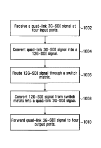
[96] FIG. 10 is a flow chart illustrating a method of switching according
to one
embodiment. This method is performed by a routing apparatus, which may (for
example) be
routing switcher 350 or routing switcher 902. In step 1002, a quad-link 3G-SDI
signal is received
at four input ports. In step 1004, the quad-link 3G-SDI signal is converted
into a corresponding
120-SDI signal within the apparatus. In step 1006, the corresponding 12G-SDI
signal is routed
through a switch matrix. Optionally, in step 1008, a 120-SDI signal from the
switch matrix is
converted into a corresponding quad-link 3G-SDI signal, and in step 1010, the
corresponding
quad-link 3G-SDI signal is forwarded to four output ports.
[97] Although the foregoing has been described with reference to certain
specific
embodiments, various modifications thereof will be apparent to those skilled
in the art without
departing from the scope of the claims appended hereto.
[98] As one example, the routing switcher 350 or routing switcher 902 are
described as
having the capability to perform all of: conversion between quad-link 3G-SDI
and 12G-SDI
(accommodating both quadrant mapping and two sample interleave mapping quad-
link 3G-SDI
format), link healing, de-skewing, and up/down sampling. However, embodiments
are also
contemplated in which only one or a subset of all of such capabilities are
provided in the routing
switcher. The input processor 390 and output processor 392 may also perform
additional
processing not described above, such as clock re-timing.
26
CA 02941282 2016-09-08
Agent's Ref: 52868-93
= [99] As another example, the embodiments described above are
explained in the
context of a routing switcher. However, the methods described herein may also
be implemented
in a production switcher or a master control switcher. More generally, the
methods described
herein may be performed by a routing apparatus.
[100] Finally, it will be appreciated that any module, component, or
device exemplified
herein that executes instructions (e.g. the input and output processors of the
routing switcher in
some embodiments) may include or otherwise have access to a non-transitory
computer/processor readable storage medium or media for storage of
information, such as
computer/processor readable instructions, data structures, program modules,
and/or other data.
A non-exhaustive list of examples of non-transitory computer/processor
readable storage media
includes magnetic cassettes, magnetic tape, magnetic disk storage or other
magnetic storage
devices, optical disks such as compact disc read-only memory (CD-ROM), digital
video discs or
digital versatile disc (i.e. DVDs), Blu-ray DiscTM, or other optical storage,
volatile and non-
volatile, removable and non-removable media implemented in any method or
technology,
random-access memory (RAM), read-only memory (ROM), electrically erasable
programmable
read-only memory (EEPROM), flash memory or other memory technology. Any such
non-
transitory computer/processor storage media may be part of a device or
accessible or connectable
thereto. Any application or module herein described may be implemented using
computer/processor readable/executable instructions that may be stored or
otherwise held by
such non-transitory computer/processor readable storage media.
27