Note: Descriptions are shown in the official language in which they were submitted.
CA 02942007 2016-09-08
WO 2015/142324 PCT/US2014/031178
HYBRID THREE-LEVEL NPC THYRISTOR CONVERTER WITH CHAIN-LINK
STRINGS AS INNER AC SWITCHES
BACKGROUND
[0001] Embodiments of invention relates to power converters and more
specifically to a
multilevel converter.
[0002] In the last few decades, the field of power conversion has grown
tremendously due to
its imminent advantages in motor drives, renewable energy systems, high
voltage direct current
(HVDC) systems, and the like. A power converter which converts electrical
energy from one
form (e.g., alternating current (AC) or direct current (DC)) to another form
(e.g., DC or AC)
utilizes various power electronic devices. Examples of power electronic
devices are insulated
gate bipolar transistors (IGBTs) and thyristors.
[0003] Thyristors have very low conduction losses compared with other power
electronic
devices such as IGBT. In addition, thyristors can guarantee to fail short, so
for the applications
which need to connect power electronic devices in series to block high
voltage, a system can
continue operating even if one or more thyristors fail. This advantage of
thyristors enables a
true redundant design, leading to much higher system reliability. These two
advantages make the
thyristor an ideal device for the HVDC application which requires high
voltage, high efficiency
and high reliability. However, thyristors are only partially controllable
devices and thus cannot
be turned off as fully controllable devices such as IGBT. Therefore,
thyristors are generally
used in a load commutated converter (LCC) based classic HVDC systems, in which
thyristors
are turned off with the help of an AC grid.
[0004] Due to the switching limitations of thyristors, IGBTs are usually
considered as the
main workhorse for a voltage source converter (VSC) based HVDC system. The VSC
based
HVDC system compared with the LCC based classic HVDC has many advantages: 1)
can
support passive network, or act as the grid for an island; 2) can control
reactive power
independent from active power. However, IGBTs lack the above mentioned
advantages of
thyristors.
[0005] Therefore, there still exists a need for an economically more viable
as well as
technically reliable and efficient alternative solutions for voltage source
converters.
1
CA 02942007 2016-09-08
WO 2015/142324 PCT/US2014/031178
BRIEF DESCRIPTION
[0006] In accordance with an embodiment of the present technique, a method
for power
conversion is provided. The method includes coupling a first string to a
second string via a first
connecting node and a second connecting node to form at least one leg of a
power converter.
The first string is operatively coupled across a first bus and a second bus
and comprises a first
branch and a second branch coupled via a third connecting node. Furthermore,
the first branch
and the second branch include a plurality of controllable semiconductor
switches and the second
string comprises a first chain link and a second chain link coupled via an
alternating current
phase bus and includes a plurality of switching units. The method also
includes controlling the
first chain link and/or the second chain link to generate a negative voltage
across at least one of
the plurality of controllable semiconductor switches during a switch turn off
process.
[0007] In accordance with another embodiment of the present technique, a
power converter
including one or more phase legs is provided. Each of the one or more phase
legs comprises a
first string comprising a first branch and a second branch including a
plurality of controllable
semiconductor switches, a first connecting node, and a second connecting node,
wherein the first
string is operatively coupled across a first bus and a second bus and the
second branch is
operatively coupled to the first branch via a third connecting node. Each of
the one or more
phase legs also include a second string operatively coupled to the first
string via the first
connecting node and the second connecting node, wherein the second string
comprises a first
chain link and a second chain link including a plurality of switching units,
and wherein the
second chain link is operatively coupled to the first chain link via an
alternating current phase
bus. The power converter further includes a controller configured to control a
switch turn-off
process of at least one of the plurality of controllable semiconductor
switches by regulating the
first chain link and the second chain link; wherein the first chain link
and/or the second chain
link are utilized to generate a negative voltage across the at least one
controllable semiconductor
switch during the switch turn off process.
DRAWINGS
[0008] These and other features, aspects, and advantages of the present
invention will
become better understood when the following detailed description is read with
reference to the
accompanying drawings in which like characters represent like parts throughout
the drawings,
wherein:
2
CA 02942007 2016-09-08
WO 2015/142324 PCT/US2014/031178
[0009] FIG. 1 is a diagrammatical representation of a system for power
conversion;
[0010] FIG. 2 is a diagrammatical representation of an exemplary embodiment of
a modular
embedded multilevel converter (MEMC) for use in the system of FIG. 1,
according to aspects of
the present disclosure;
[0011] FIG. 3 is a diagrammatical representation of an exemplary embodiment of
a switching
unit for use in the portion of the power converter of FIG. 2, according to
aspects of the present
disclosure;
[0012] FIG. 4 is a diagrammatical representation of another embodiment of a
switching unit
for use in the portion of the power converter of FIG. 2, according to aspects
of the present
disclosure;
[0013] FIG. 5 is a diagrammatical representation of a phase leg and
operating states of the
phase leg, according to aspects of the present disclosure;
[0014] FIG. 6 is a diagrammatical representation of a section of the
modular embedded
multilevel converter (MEMC) of FIG. 2, according to aspects of the present
disclosure;
[0015] FIG. 7 is a flow chart representation of a method for commutating a
thyristor in a
converter having a chain link comprising switching units, according to aspects
of the present
disclosure; and
[0016] FIG. 8 is a diagrammatical representation of progression of one
phase leg from a
positive state to a negative state, according to aspects of the present
disclosure.
DETAILED DESCRIPTION
[0017] Unless defined otherwise, technical and scientific terms used herein
have the same
meaning as is commonly understood by one of ordinary skill in the art to which
this disclosure
belongs. The terms "first", "second", and the like, as used herein do not
denote any order,
quantity, or importance, but rather are used to distinguish one element from
another. Also, the
terms "a" and "an" do not denote a limitation of quantity, but rather denote
the presence of at
least one of the referenced items. The term "or" is meant to be inclusive and
mean one, some, or
all of the listed items. The use of "including," "comprising" or "having" and
variations thereof
herein are meant to encompass the items listed thereafter and equivalents
thereof as well as
additional items. The terms "connected" and "coupled" are not restricted to
physical or
3
CA 02942007 2016-09-08
WO 2015/142324 PCT/US2014/031178
mechanical connections or couplings, and can include electrical connections or
couplings,
whether direct or indirect. Furthermore, the terms "circuit" and "circuitry"
and "controller" may
include either a single component or a plurality of components, which are
either active and/or
passive and are connected or otherwise coupled together to provide the
described function.
[0018] As will be described in detail hereinafter, various embodiments of
an exemplary
system for power conversion and method for power conversion are presented. By
employing the
power converter and the method for power conversion described hereinafter, a
multilevel
converter is provided. In one example, the power converter may include a
modular multilevel
embedded converter. The term multilevel converter, as used herein, is used to
refer to a
converter that converts one form of input voltage/current to another form of
output
voltage/current with very low distortion.
[0019] Turning now to the drawings, by way of example in FIG. 1, a system 100
for
converting power is depicted. In one embodiment, the system 100 for converting
power may
include a source 102, a power converter 104, and a grid/utility/load 106. The
term source, as
used herein, is used to refer to a renewable power source, a non-renewable
power source, a
generator, a grid, and the like. Also, the term load, as used herein, may be
used to refer to a grid,
an electrical appliance, and the like. In addition, the power converter 104
may be a multilevel
converter. In one embodiment, the source 102 may be operatively coupled to a
first terminal
(not shown) of the power converter 104. A second terminal (not shown) of the
power converter
104 may be operatively coupled to the load 106. The first terminal and the
second terminal may
be alternatively employed as an input terminal or an output terminal of the
power converter 104.
[0020] Also, the system 100 may include a controller 108. The controller
108 may be
configured to control the operation of the power converter 104, in one
embodiment. By way of
example, the controller 108 may be configured to control the operation of the
power converter
104 by controlling switching of a plurality of semiconductor switches of the
power converter
104. Furthermore, in one embodiment, the system 100 may also include other
circuit
components (not shown) such as, but not limited to, a circuit breaker, an
inductor, a
compensator, a capacitor, a rectifier, a reactor, a filter, and the like.
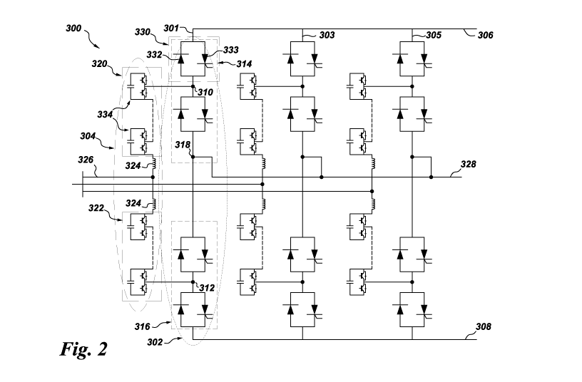
[0021] Referring now to FIG. 2, a diagrammatical representation of an
exemplary
embodiment of a modular embedded multilevel converter (MEMC) 300 for use in
the system of
FIG. 1 according to aspects of the present disclosure is depicted. In one
embodiment, MEMC
300 includes three legs 301, 303 and 305 respectively. The three legs 301, 303
and 305 are for
4
CA 02942007 2016-09-08
WO 2015/142324 PCT/US2014/031178
three different phases and thus can also be called as phase legs. Furthermore,
each phase leg
301, 303 and 305 of the MEMC may include a first string 302 and a second
string 304. It should
be noted that even though in FIG. 2, certain referral numerals are shown for
only one leg 301,
they can be equally applicable to other two phase legs 303 and 305. More
particularly, the first
string 302 may be operatively coupled to the second string 304 to form the leg
301.
Furthermore, the first string 302 may be operatively coupled between a first
bus 306 and a
second bus 308. In one embodiment, the first bus 306 may include a positive DC
bus and the
second bus 308 may include a negative DC bus. The second string 304 may be
operatively
coupled to the first string 302 via a first connecting node 310 and a second
connecting node 312.
Also, the first string 302 may include a first branch 314 operatively coupled
to a second branch
316 via a third connecting node 318. Similarly, the second string 304 may
include a first chain
link 320 operatively coupled to a second chain link 322 via at least one AC
phase 326 and an
inductor 324. The term "chain link" here refers to a series string of
switching modules such as
elements 334. In an embodiment, inductor 324 is a split inductor i.e.,
inductor 324 is split into
two parts. The third connecting node 318 may be operatively coupled to a third
bus 328.
[0022] In addition, the first phase leg 301 may be operatively coupled to
the second phase leg
303 via the third connecting node 318. Furthermore, in one example, the third
connecting nodes
318 of each of the three first strings 302 may be operatively coupled to each
other. The third
bus 328 is a middle bus which may be floating or grounded or a high impedance
grounded bus.
However, in another embodiment, for applications such as machine drives, the
third connecting
nodes 318 of each of the three first strings 302 may be operatively coupled to
a neutral bus.
Moreover, the three legs 301, 303, 305 may be operatively coupled between the
first bus 306
and the second bus 308.
[0023] In one embodiment, the third bus 328 may be at a negative potential
with respect to
the first bus 306 and at a positive potential with respect to the second bus
308. Also, the first
string 302 may include a plurality of controllable semiconductor switches 330.
In the example
of FIG. 2, the plurality of controllable semiconductor switches may include
partially controllable
semiconductor switches. However, in another embodiment, the plurality of
controllable
semiconductor switches may include fully controllable semiconductor switches.
Moreover, the
plurality of controllable semiconductor switches may include a combination of
partially
controllable semiconductor switches and fully controllable semiconductor
switches. By way of
a non-limiting example, the first string 302 may include partially
controllable semiconductor
switches, fully controllable semiconductor switches, or a combination of
partially controllable
CA 02942007 2016-09-08
WO 2015/142324 PCT/US2014/031178
semiconductor switches and fully controllable semiconductor switches.
Furthermore, in one
example, the first branch 314 of the first string 302 may include two
controllable semiconductor
switches 330. Similarly, the second branch 316 of the first string 302 may
include two
controllable semiconductor switches 330. The controllable semiconductor switch
330 may
include a power diode 332 in combination with a thyristor 333 or a silicon
controlled rectifier.
In other embodiments, controllable semiconductor switch 330 may include a
thyristor, an anti-
parallel thyristor and the like. In one embodiment, controllable semiconductor
switche 330 may
comprise one or more thyristors connected in series to develop a proper
voltage rating. It should
be noted that for ease of explanation, embodiments in subsequent paragraphs
are described with
respect to thyristors, however, the technique presented herein is equally
applicable to other
controllable semiconductor switches as discussed above.
[0024] The inductors 324 in each leg 301, 303 and 305 are operatively
coupled to at least one
alternating current (AC) phase (e.g., A, B, and C). In addition, the first
chain link 320 and the
second chain link 322 of the second string 304 may include a plurality of
switching units 334
connected in series to each other. The switching unit 334 may be a combination
of a plurality of
fully controllable semiconductor switches and an energy storage device. The
fully controllable
semiconductor switches may include an insulated gate bipolar transistor
(IGBT), a metal oxide
semiconductor field effect transistor (MOSFET), a field effect transistor
(FET), a gate turn-off
thyristor, an insulated gate commutated thyristor (IGCT), an injection
enhanced gate transistor
(IEGT), a silicon carbide based switch, a gallium nitride based switch, a
gallium arsenide based
switch, or equivalents thereof
[0025] Referring now to FIG. 3, diagrammatical representation 400 of an
exemplary
embodiment of a switching unit such as the switching unit 334 of FIG. 2 is
depicted. In the
presently contemplated configuration, the switching unit 400 may be referred
to as a half bridge
converter and includes fully controllable semiconductor switches 402 and 404,
an energy storage
device 406, a first connector 408, and a second connector 410. As previously
noted, the fully
controllable semiconductor switches 402, 404 may include an IGBT, a MOSFET, a
FET, an
IEGT, a gate turn-off thyristor, an IGCT, a silicon carbide based switch, a
gallium nitride based
switch, a gallium arsenide based switch, or equivalents thereof Moreover, each
of the fully
controllable semiconductor switches 402, 404, may also include a power diode
412 that may be
inbuilt and antiparallel to the fully controllable semiconductor switches 402
and 404. The
inbuilt power diodes 412 may provide a freewheeling path. These power diodes
412 may also
be referred to as freewheeling diodes.
6
CA 02942007 2016-09-08
WO 2015/142324 PCT/US2014/031178
[0026] Also, in one non-limiting example, the energy storage device 406 may
include a
capacitor. In the example of FIG. 3, the fully controllable semiconductor
switch 402 may be
operatively coupled in series to the energy storage device 406 to form a first
limb 414. Also, the
other fully controllable semiconductor switch 404 forms a second limb 416. The
second limb
416 may be operatively coupled in parallel to the first limb 414.
Additionally, the first limb 414
and the second limb 416 may be operatively coupled between the first connector
408 and the
second connector 410. Although the example of FIG. 3 depicts the switching
units 400 in a half
bridge converter configuration as including two fully controllable
semiconductor switches, and
one energy storage device, use of other numbers of fully controllable
semiconductor switches
402, 404, and energy storage devices 406 is also contemplated. In one
embodiment, some or all
of the switching units may be arranged to form a full bridge converter
configuration as will be
described in Fig. 4.
[0027] Furthermore, in one non-limiting example, when the fully
controllable semiconductor
switch 402 is activated and the fully controllable semiconductor switch 404 is
deactivated, the
energy storage device 406 may appear across the first connector 408 and the
second connector
410. Consequently, the charge across the energy storage device 406 appears as
a voltage across
the first connector 408 and the second connector 410. Alternatively, when the
fully controllable
semiconductor switch 404 is activated and the fully controllable semiconductor
switch 402 is
deactivated, the first limb 414 is bypassed, thereby providing zero voltage
across the first
connector 408 and the second connector 410. Hence, by controlling the
switching of the fully
controllable semiconductor switches 402 and 404 in the plurality of switching
units 334 on the
second string 304 of FIG. 2, the voltage developed across the second string
304 may be
regulated.
[0028] Referring now to FIG. 4, diagrammatical representation 500 of an
alternative
embodiment of switching unit 334 of FIG. 2 is depicted. In the presently
contemplated
configuration, the switching unit 400 may be referred to as a full bridge
converter and may
include fully controllable semiconductor switches 502, 504, 514 and 516, an
energy storage
device 506, a first connector 508, and a second connector 510. As previously
noted, the fully
controllable semiconductor switches 502, 504, 514 and 516 may include an IGBT,
a MOSFET,
a FET, an IEGT, a gate turn-off thyristor, an IGCT, a silicon carbide based
switch, a gallium
nitride based switch, a gallium arsenide based switch, or equivalents thereof
Moreover, each of
the fully controllable semiconductor switches 502, 504, 514, 516, may also
include a power
diode 512, 511, 513 or 515 respectively that may be inbuilt and antiparallel
to the fully
7
CA 02942007 2016-09-08
WO 2015/142324 PCT/US2014/031178
controllable semiconductor switches. As can be seen, compared to switching
unit 400 of Fig. 3,
switching unit 500 includes two additional fully controllable semiconductor
switches and an
output of switching unit 500 appears across first connector 508 and second
connector 510. In
one embodiment, fully controllable semiconductor switches 502, 504, 514, 516
are controlled to
regulate a voltage across first connector 508 and second connector 510.
Contrary to switching
unit 400, switching unit 500 can produce 3 voltage levels across first
connector 508 and second
connector 510. The three voltages levels would be a zero voltage level and
positive and
negative polarity voltage levels, wherein the positive and the negative
polarity voltage levels
represent a charge across energy storage device 506.
[0029] Referring to Fig. 5, a diagrammatical representation 550 of a phase
leg 552, such as
the leg 301 of FIG. 2, and operating states of phase leg 552 is depicted. For
ease of
understanding, FIG. 5 will be described with respect to FIG. 2. In general,
during operation of
MEMC 300 (Fig. 2), there may be at least three operating states positive,
negative and zero for
each phase leg 301, 303 and 305. In Fig. 5, a first chain link, such as the
first chain link 320 of
FIG. 2 and a second chain link, such as the second chain link 322 of FIG. 2 is
represented by
voltage sources Vp and V., respectively. As noted hereinabove, the first and
the second chain
links include a plurality of switching units (not shown), however, for ease of
explanations the
first and the second chain links have been replaced by voltage sources Vp and
V.. In other
words, the voltage of voltage sources Vp and V. depend on the switching of the
fully
controllable semiconductor switches corresponding to the plurality of
switching units 334 in
chain links 320 and 322 of Fig. 2. Also, in the presently contemplated
configuration a first
string, such as the first string 302 of FIG. 2 includes four controllable
semiconductor switches
represented as T1, T2, T3 and T4.
[0030] Fig. 5 also depicts operating states such as a positive state 554, a
negative state 558
and a zero state 556 of phase leg 552. As can be seen, the positive state 554
includes switching
on first and third thyristors T1 T3 and switching off second and fourth
thyristors Tz, T4.
Furthermore, the negative state 558 includes switching on second and fourth
thyristors Tz, T4
and switching off first and third thyristors T1, T3 and the zero state 556
includes switching on
second and third thyristors Tz, T3 and switching off first and fourth
thyristors T1, T4. Depending
on the state, voltage sources Vp and V. are connected between at least one AC
phase
(represented by voltage Vphs) and one of the three buses, a positive DC bus
(represented by
voltage +Vac), a negative DC bus (represented by voltage ¨Vac) or a middle bus
(represented by
voltage V..d) via inductor L. For example, in the positive state 554, voltage
source Vp is
8
CA 02942007 2016-09-08
WO 2015/142324 PCT/US2014/031178
connected between AC phase voltage Vphs and positive DC bus voltage +Vde. At
the same time,
voltage source V. is connected between AC phase voltage Vphs and middle bus
voltage Vima
which may be at a negative potential with respect to positive DC bus voltage
+Vac.
[0031] During negative state 558, voltage source Vp is connected between AC
phase voltage
Vphs and middle bus voltage V..d whereas voltage source V. is connected
between AC phase 326
and the negative DC bus. During zero state 556, voltage source Vp and V. both
are connected
between AC phase voltage Vphs and middle bus voltage V.I. As can be seen from
Fig. 5, for
transitioning from one state to another state one or more thyristors may need
to be switched off
or commutated. For example, during the positive state 554, thyristors T1 and
T3 are conducting
and to begin the transition to the negative state 558, first thyristor T1 need
to be switched off
then thyristor T2 need to be switched on and then again thyristor T3 need to
be switched off
[0032] In one embodiment, to force commutate a thyristor, a thyristor
current is forced to
zero and an anode voltage of the thyristor with respect to its cathode is held
negative for a
designated turn-off time tq. Furthermore, a rate of rise of the anode voltage
after being kept at
the negative voltage for time tq is limited to a designated voltage ramp
level. In one
embodiment, the designated hold-off time and the designated ramp level both
are determined
based on thyristor characteristics and overall system parameters.
[0033] In one embodiment of the present technique, voltages across
switching units 334 in
chain links 320 and 322 of Fig. 2 are regulated to control the thyristor
commutation (also
referred to as the switch or the thyristor turn off process). It should be
noted that even though
present discussion provides thyristor commutation examples in the context of
the MEMC
converter, the technique for thyristor commutation disclosed herein can be
applied to any other
power conversion device utilizing a thyristor in combination with a chain link
having switching
units.
[0034] Referring now to FIG. 6, diagrammatical representation of a section 600
of modular
embedded multilevel converter (MEMC) 300 of FIG. 2 is depicted. For ease of
understanding,
FIG. 6 will be described with respect to FIGs. 1 and 2. In the section shown,
thyristor 333,
diode 332, inductor 324 and a chain link 602 of switching units 334 are
depicted. An example
of switching unit 334, which is a half bridge converter configuration 400 as
in Fig. 3 is also
depicted and positive DC bus voltage +Vde as well as AC phase voltage Vphs is
also shown. As
described earlier, the switching unit 334 could also be a full bridge
converter configuration 500
as in Fig. 4. Furthermore, chain link 602 may also include a combination of
half bridge
9
CA 02942007 2016-09-08
WO 2015/142324 PCT/US2014/031178
converter configurations and full bridge converter configurations. For ease of
explanation, a
positive polarity of voltage across thyristor 333 is shown as +/- sign and a
positive direction of
current through thyristor 333 is shown as a downward arrow in Fig. 6.
Furthermore, an
equivalent voltage source Vp for chain link 602 is also shown. As discussed
earlier, voltage of
voltage source Vp depends on control of switching units 334. When thyristor
333 is switched
ON, a voltage VT across the thyristor is positive and close to zero and a
current iT through the
thyristor is positive. It should also be noted that, for other thyristors in
MEMC 300 which are not
shown in section 600, each thyristor will be in series with at least one chain-
link when it is
conducting. The chain link may be from the same phase leg or from a different
phase leg.
Furthermore, thyristors which are not conducting at the same time may share a
common chain-
link.
[0035] In an embodiment, controller 108 is utilized to control the overall
operation of MEMC
300 including the thyristor commutation. In one embodiment, to switch off
thyristor 333,
controller 108 first removes a gate signal of thyristor 333. However, it
should be noted that
thyristor 333 would not switch off merely by removing its gate signal but the
thyristor current iT
also needs to be reduced to zero. Furthermore, thyristor current iT would go
to zero only when
the thyristor voltage VT is negative i.e., when the voltage (Vphs+Vp) is
higher than voltage +Vac,
where voltage Vphs is defined by voltage V. (Fig. 5). Since switching units
334 have energy
storage components (e.g., element 406 of Fig. 2), current iT can be regulated
to zero without the
help of any external power source, such as an AC grid which is generally
needed in conventional
thyristor commutation. Thus, controller 108 controls switching units 334 in
chain link 602 so as
to make voltage Vp higher than voltage +Vde. In addition, when current iT is
decreasing,
controller 108 controls a current decrease ramp rate diT/dt of thyristor
current iT as per thyristor
characteristics requirements. For example, in one embodiment, the thyristor
characteristics may
require that decrease slope diT/dt of thyristor current iT should be less than
or equal to 10A/ns.
Accordingly, controller 107 regulates voltage Vp and controls the decrease
slope.
[0036] It should be noted that although it is stated here that thyristor
current iT is regulated to
zero with the help of chain-link 602, more than one chain link in the MEMC
converter may be
utilized together to regulate the thyristor current iT to zero. For example,
voltage sources Vp and
V. both are used in sync to commutate a thyristor.
[0037] As discussed above to switch off thyristor 333, the thyristor
current iT should reduce
to zero. Controller 108 can determine a time point when thyristor current iT
reaches zero by
different methods. In an embodiment where there is an anti-parallel diode 332
with thyristor
CA 02942007 2016-09-08
WO 2015/142324 PCT/US2014/031178
333 to carry the negative current as shown in Fig. 6, controller 108
determines such time point
based on measurement of the negative current in the anti-parallel diode 332.
However, if there
no path for negative current then another way controller 108 detects the time
point for zero
thyristor current is based on measurement of the voltage across the thyristor.
[0038] If after the thyristor 333 is switched off, thyristor voltage VT is
going to be negative
then the whole process to switch off thyristor may be over. However, if
thyristor 333 needs to
block a positive voltage after it is switched off then the controller 108
keeps applying the
negative thyristor voltage VT for a time period tq. Time period tq may also be
referred to as a
switch off time i.e., a time period which needs to lapse after thyristor
current iT reaches zero and
before thyristor voltage VT can be made positive. Time period tq can be
affected by many
factors and is chosen based on thyristor characteristics and overall system
parameters.
Furthermore, after time period tq, controller 108 regulates a rate of
reapplication of the positive
voltage on the thyristor, dv/dt to a designated ramp level which again is
determined based on
thyristor characteristics and overall system parameters.
[0039] Referring to FIG. 7, a flow chart representation 650 of a method for
commutating a
thyristor in a converter having a chain link comprising switching units is
depicted. For ease of
understanding, FIG. 7 will be described with respect to FIGs. 1 and 6. The
method starts with
step 652 where the thyristor is in ON state i.e., thyristor current iT and
thyristor voltage VT are
greater than zero. At step 652, a gate signal to the thyristor is removed and
then thyristor current
iT is slowly reduced with a controlled diT/dt slope. As mentioned above, to
reduce thyristor
current iT, controller 108 applies a negative voltage across the thyristor. In
other words,
controller 108 controls switching units 334 in chain link 602 so as to make
voltage Vp higher
than voltage +Vde. At step 656, it is determined whether thyristor current iT
has indeed reduced
to zero. If thyristor current iT is not reduced to zero then step 656 may be
repeated after some
time or the method may move back to step 654 to remove gate signal to the
thyristor. However,
if thyristor current iT is indeed zero then the method moves to step 658. At
step 658, it is
determined whether thyristor voltage VT will be greater than zero. If
thyristor voltage VT will be
greater than zero then the method moves to step 660 else the method moves to
step 664 which
discloses that the thyristor is in OFF state. At step 660, controller 108
keeps applying the
negative voltage across the thyristor for a time period tq which is a switch
off time. After time
period tq, if needed at step 662 a positive voltage is applied across the
thyristor with a controlled
dv/dt rate and then step 664 discloses that the thyristor is in OFF state.
11
CA 02942007 2016-09-08
WO 2015/142324 PCT/US2014/031178
[0040] Referring to FIG. 8, a diagrammatical representation 700 of
progression of one phase
leg 702 (i.e., phase a) from a positive state to a negative state is depicted.
For ease of
understanding, FIG. 8 will be described with respect to FIGs. 2, 5 and 6. Fig.
8 shows voltage
waveforms Va., Vb and V, corresponding to three AC phases a, b and c
respectively. Chain link
currents iap and an corresponding to first and second chain links of the phase
leg a are also
depicted. Furthermore, first and second chain link voltage sources related to
three phase legs
702, 704, 706 (corresponding to phases a, b and c) are represented by voltage
sources Vap, Van,
Vbp, Vbn, Veil and Vea respectively.
[0041] Phase leg 702 transitions from a positive state to a negative state
via a zero state. In
the zero state, voltage sources Vp and Va both are connected between AC phase
voltage Va and
middle bus voltage Vnud. If the voltage sources Vp and Va comprise only
unidirectional voltage
modules (e.g., half bridge converter 400 of Fig. 3 which is capable of
producing only positive
and zero level voltages), then during zero state the AC phase voltage Va is at
the same voltage as
the middle bus voltage Vaud. However, to transition from zero state to
negative state and so to
commutate thyristor T3, at least one of the voltage sources Vp or Va should be
capable of
developing some negative voltage. Therefore, voltage sources Vp and Va may
include at least
some bidirectional voltage modules (e.g., full bridge converter 500 of Fig. 4
which is capable of
producing positive as well as negative level voltages along with zero level
voltage). It should
also be noted that the extent of the bidirectional voltage capability of the
chain link plays a
major role in the time it takes for the phase leg to transition from one state
to another.
[0042] It can be seen from Fig. 8 that when phase leg 702 is transitioning
from the positive
state to the negative state, phase leg 704 is in the positive state and phase
leg 706 is in the
negative state. In order to support the full DC bus voltage (i.e., +Vde to -
Vde) it is desired that at
least one phase leg be in the positive state and one phase leg be in the
negative state
simultaneously. Thus, in the present embodiment, phase leg 704 is effectively
connected in
series with the phase leg 706 across the entire DC bus formed by the positive
DC bus and the
negative DC bus. In Fig. 8, the transition of phase leg 702 from the positive
state to the negative
state via the zero state is shown in five stages. In the first stage 708,
phase leg 702 is in the
positive state; in the third stage 712, phase leg 702 is in the zero state and
in the fifth stage 716,
phase leg 702 is in the negative state. Furthermore, second stage 710 is a
middle stage between
the positive and the zero state where thyristor T1 (Fig. 5) commutates and
fourth stage 714 is
another middle stage between the zero and the negative state where thyristor
T3 commutates.
12
CA 02942007 2016-09-08
WO 2015/142324 PCT/US2014/031178
[0043] As discussed earlier, the first step in the transition of phase leg
702 from the positive
state to the negative state is to turn off thyristor Tl. In other words,
controller 108 removes the
gate signal to thyristor T1 if it present. In the next step, Controller 108
drives the current in
thyristor T1 to zero at a controlled maximum rate of change. This is
equivalent to driving the
current in the upper chain link ip to zero or below at some designated current
decrease ramp rate
di/dt. In order to support the required phase leg current when current ip is
reducing to zero, the
lower chain link current in also changes in the opposite direction at the same
di/dt. For this
purpose, controller 108 generates and controls a circulating current 718 among
voltage sources
Vap, Van, Vbp and Vbn as shown in Fig. 8.
[0044] After the upper chain link current ip and thus thyristor T1 current
crosses through zero,
controller 108 holds the thyristor voltage VT at zero or slightly negative
volts for the required
turn-off time tq. In other words, controller 108 controls the upper chain link
voltage to be equal
to or slightly greater than the difference between the phase voltage Va and DC
link voltage Vdc.
During this stage, the anti-parallel diode of T1 would conduct and carry the
negative current the
upper chain link. After the turn-off time tq, controller 108 increases the
upper chain link voltage
to the middle bus voltage under a controlled dv/dt rate. Once the thyristor
voltage VT is brought
down to the middle bus voltage Vnud, controller 108 provides a gate pulse to
thyristor T2 to
switch it on for connecting the upper chain link to the middle bus. This
completes the transition
of phase leg 702 from the positive state to the zero state. The controller 108
then utilizes similar
steps for thyristor T3 to transition from the zero state to the negative
state.
[0045] The various embodiments of the power converter and the methods of power
conversion described hereinabove aid in developing multilevel power
converters, thereby
allowing generation of high power/voltage/current output. Furthermore, the use
of thyristors in
the power converter provides a less expensive and efficient system compared to
a conventional
modular power converter. One of the advantages of the present technique is
that it does not need
any external power source such as an AC power grid for the thyristor
commutation process and
thus enhances control flexibility of the converter.
[0046] While only certain features of the invention have been illustrated
and described
herein, many modifications and changes will occur to those skilled in the art.
It is, therefore, to
be understood that the appended claims are intended to cover all such
modifications and changes
as fall within the true spirit of the invention.
13