Note: Descriptions are shown in the official language in which they were submitted.
CA 02942044 2016-09-08
WO 2015/142478
PCT/US2015/017010
HEAVILY PHOSPHOR LOADED LED PACKAGE
i. Field of the Invention
100011 The present disclosure relates generally to light emitting diodes
(LEDs) that are
phosphor loaded. More particularly, the present disclosure relates to heavily
phosphor loaded
LED packages having higher stability and a method for increasing the stability
of heavily
phosphor loaded LED packages.
11. Background of the Invention
100021 LEDs are semiconductor light emitters often used as replacements for
other light
sources, such as incandescent lamps. They are particularly useful as
illumination sources in
applications where discrefized or highly concentrated light is desired. The
color of light
produced by an LED package is dependent on the type of semiconducting material
used in its
manufacture and, where a phosphor system is used, the phosphor blend that is
used.
100031 Colored semiconductor LEDs, including light emitting diodes and
lasers (both are
generally referred to herein as LEDs), have been produced from Group III-V
alloys such as
gallium nitride (GaN). With reference to the GaN-based LEDs, light is
generally emitted in
the UV to green range of the electromagnetic spectrum. Until more recently,
LEDs have not
been suitable for lighting uses where a bright white light is needed, due to
the inherent color
of the light produced by the LED.
100041 Phosphors convert radiation (energy) to visible light. Different
combinations of
phosphors provide different colored light emissions. The color of the
generated visible light is
dependent on the particular components of the phosphor material. The phosphor
material may
include only a single phosphor composition or two or more phosphors of basic
color, for
example a particular mix with one or more of a yellow and red phosphor to emit
a desired
color (tint) of light. As used herein, the terms "phosphor" and "phosphor
material" may be
used to denote both a single phosphor composition as well as a blend of two or
more
phosphor compositions.
100051 In typical applications where "white" light is desired, phosphors
are used in
conjunction with LEDs to provide an acceptable net emission spectrum of
desired
characteristics. "White" light is typically defm.ed as being close to the
black body locus in
1
CA 02942044 2016-09-08
WO 2015/142478
PCT/US2015/017010
color in regions of Correlated Color Temperatures (CCT) of 2500K to 6000K. For
example,
in a typical luminaire application, LEDs made from InGaN (Indium Gallium
Nitride) that
emit in the blue region of the electromagnetic spectrum are used in
conjunction with yellow,
green, and red phosphors to provide composite spectral outputs ranging from
about 2500 K
CCT to above 6000 K CCT. The resultant color temperature and color point in
the CIE
tristimulus plot depends on the output spectral power and wavelength of the
diode emitter,
the blend ratio, conversation characteristics, and amounts of phosphors used.
100061 US Patent No. 7,497,973 discloses LEDs including a semiconductor
light source
and a phosphor material including a complex phosphor activated with Mn4 . The
particular
phosphor material is K2[SIF6]:Mn4+ (potassium fluoride silicon or PH).
100071 Another LED uses a combination of the PFS phosphor and the phosphor
BSY
(blue-shifted Ythium Aluminum Garnet (YAG)). This combination is called BSY-
PFS and it
yields a white light. One preferred embodiment of an LED package using a BSY-
PFS
combination is a mid-power LED package (<1W), used as an exemplary embodiment
herein.
The package has been fabricated using Nichia Mint Phosphor (BSY) and GE PFS
phosphor
in a Nichia 757 package. The usage of garnet phosphors in white LEDs is
covered under US
Patent Nos. 5,998,925 and 7,026,756. To those skilled in the art it will be
evident that the
implementation of the inventive elements is not limited to the Nichia 757. The
invention can
be implemented in a number of different LED packages where PFS is used in
conjunction
with a BSY phosphor or a spectrally similar phosphor.
100081 Accordingly, the use of phosphors in LED packages provides
advantages and is
common. However, in general, LED packages that include PFS phosphors exhibit
long term
color and lumen stability issues. For example, the color requirement of the
BSY-PFS system
at 4000K Hi CItl (color rendering index) necessitates very high phosphor
loading of the
silicone/phosphor disk/mold. In reliability tests in the presence of humidity,
the resulting
visible radiation from the energized LED packages shift color. Mainly the red
component of
the spectral power distribution loses intensity gradually over operating time.
The high
phosphor loading also results in side wall "trench" formations and other
effects that result in
net color point shift.
2
CA 02942044 2016-09-08
WO 2015/142478
PCT/US2015/017010
100091 The above-described shortcomings significantly limit the usefulness
of PSF
LEDs such as the BSY-PSF LED. Therefore, it would be useful to have LED
package level
improvements that mitigate color instability issues.
100101 This invention relates to improving the stability of LED packages
using PFS
phosphor. Generally in such packages the phosphor loading is high as mentioned
above.
High loading in this context refers to phosphor to silicone weight ratios of
20% and higher.
III. Sutnmary of the Invention
100111 In at least one aspect, the present disclosure provides a heavily
phosphor loaded
LED package having higher stability. Preferably the LED package is a low to
medium power
LED. One exemplary embodiment is the Nichia 757 mid power LED package, which
is
highly loaded with a BSY-PFS phosphor blend. The phosphor blend is overlayed
with a
silicone overlayer which protects the phosphor and provides an improvement in
color shin.
100121 In another embodiment, the invention provides a method to improve
the long
term stability and reliability of LED packages that employ PFS phosphor
systems. In the
method, a silicone over layer is provided on top of the silicone/ phosphor
layer.
IV. Brief Description of the Drawings
100131 FIG. 1 illustrates a schematic view of an LED of the prior art.
100141 FIG. 2 illustrates an LED package with a silicone over layer.
100151 The present disclosure may take form in various components and
arrangements of
components, and in various process operations and arrangements of process
operations. The
present disclosure is illustrated in the accompanying drawings, throughout
which like
reference numerals may indicate corresponding or similar parts in the various
figures. The
drawings are only for purposes of illustrating preferred embodiments and are
not to be
construed as limiting the disclosure. Given the following enabling description
of the
drawings, the novel aspects of the present disclosure should become evident to
a person of
ordinary skill in the art.
V. Detailed Description
100161 The following detailed description is merely exemplary in nature and
is not
intended to limit the applications and uses disclosed herein. Further, there
is no intention to
3
CA 02942044 2016-09-08
WO 2015/142478
PCT/US2015/017010
be bound by any theory presented in the preceding background or summary or the
following
detailed description. While embodiments of the present technology are
described herein
primarily in connection with PFS LED packages, and especially the Nichia 757
BSY-PFS
LED package, the concepts are also applicable to other types of phosphor
loaded LEDs and
especially with other types of heavily phosphor loaded LEDs. Specifically, the
concepts are
most applicable in LED packages where the phosphor to silicone weight ratio is
high (20%
and higher) and at least one of the phosphors exhibits sensitivity to ambient
atmospheric
constituents such as moisture.
100171 Figure 1 shows an exemplary prior art LED package 10. The package 10
comprises a light emitting diode (LED) chip 12. A phosphor and silicone blend
layer 22
overlays the chip 12. The LED chip 12 and phosphor silicone blend layer 22 are
encapsulated
with a lens 18. The LED package 10 includes an outside enclosure 30.
100181 The phosphor silicone blend layer 22 is radiationally coupled to the
LED chip 12
in the direction indicated by arrow 24. Radiationally coupled means that the
elements are
associated with each other so that at least part of the radiation emitted from
one is transmitted
to the other.
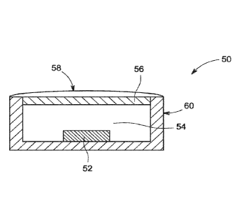
100191 One embodiment of a heavily phosphor loaded LED package 50 having
greater
stability is shown in Figure 2. The package 50 comprises a semiconductor UV or
visible
radiation source, such as a light emitting diode (LED) chip 52. A phosphor and
silicone
blend layer 54 overlays the chip 52.
100201 The package 50 may include any semiconductor visible or UV light
source that is
capable of producing white light when its emitted radiation is directed onto
the phosphor. The
preferred peak emission of the LED chip 52 will depend on the identity of the
phosphors used
and may range from, e.g., 250-550 rtm. In one preferred embodiment, however,
the emission
of the LED will be in the violet to blue-green region and have a peak
wavelength in the range
from about 420 to about 500 nm. Typically then, the semiconductor light source
comprises an
LED doped with various impurities. Thus, the LED may comprise a semiconductor
diode
based on any suitable HI-V, 11-V1 or IV-IV semiconductor layers and having a
peak emission
wavelength of about 250 to 550 nm.
4
CA 02942044 2016-09-08
WO 2015/142478
PCT/US2015/017010
100211 Although the general discussion of the exemplary structures of the
invention
discussed herein are directed toward inorganic LED based light sources, it
should be
understood that the LED chip may be replaced by an organic light emissive
structure or other
radiation source unless otherwise noted and that any reference to LED chip or
semiconductor
is merely representative of any appropriate radiation source.
100221 The phosphor silicone blend layer 54 is desirably heavily loaded
with phosphor,
especially 20% or greater by weight phosphor. The phosphor silicone blend
layer 54 is
generally about 0.2 mm in thickness. In preferred embodiments, the phosphor is
a blend of
PFS phosphor and BSY phosphor or a spectrally similar phosphor. Particularly
preferred are
the Nichia Mint phosphor (BSY) and GE PFS phosphor, desirably in a low to mid
power
LED package. An example is the Nichia 757 package.
100231 A silicone overlayer 56 is provided on top of the phosphor silicone
blend layer
54. The overlayer has a thickness of about 0.1 mm, desirably between about 0.1
and 0.5 mm.
The silicone used is desirably the same type as than in the phosphor silicone
blend layer 54.
100241 The silicone over layer 56 is desirably applied or synthetically
created from the
blend immediately following dispensing of the silicone/phosphor slurry and
subsequent
simultaneous curing to avoid separation. In a preferred embodiment, prior to
curing the
silicone phosphor blend in the LED package, the silicone protective over layer
56 can be
formed by gravitational settling of the phosphor in the silicone blend. The
settling process
can be aided by artificially creating additional gravitational force via a
centrifuge or like
device. This gravitational action physically settles a phosphor silicone blend
layer 54 down
on the LED chip 52 and allows silicone seepage to the top to form a silicone
only protective
overlayer 56.
100251 The LED chip 52 and phosphor silicone blend layer 54 may be
encapsulated with
a lens 58. The lens 58 may be, for example, an epoxy, plastic, low temperature
glass,
polymer, thermoplastic, thermoset material, resin, or other type of LED
encapsulating
material as is known in the art. Optionally, the lens 58 is a spin-on glass or
some other
material having a high index of refraction. In one preferred embodiment, the
lens 58 is a
polymer material, such as epoxy, silicone, or silicone epoxy, although other
organic or
inorganic encapsulants may be used.
CA 02942044 2016-09-08
WO 2015/142478
PCT/US2015/017010
100261 The lens 58 is preferably transparent or substantially optically
transmissive with
respect to the wavelength of light produced by the LED chip 52 and phosphor
silicone blend
material 54. In an alternate embodiment, the package 50 may only comprise an
encapsulant
material without an outer lens.
100271 The outside enclosure 60 of the LED package is typically made of
polymeric
composite material EMC (Epoxy M.oldable Compound). The LED chip 52 may be
supported, for example, by a lead frame (not shown), by the self-supporting
electrodes, the
bottom of the enclosure 60, or by a pedestal (not shown) mounted to the shell
or to the lead
frame. The LED chip 52 is electrically attached to electrical contacts at the
bottom surface of
the outside enclosure 60. It is known to those skilled in. the art that there
could be multiple
chips present in LED packages that have similar functional attributes.
100281 The silicone overlayer 56 has been quantified to provide about a 25%
improvement in package color shift as compared to the same LED package without
the
silicone overlayer due to its protection of the phosphor and isolation from
ambient
constituents such as water.
100291 Example
100301 Nichia 757 LEDs with high BSY-PFS phosphor loading (weight
proportion
Silicone:PFS:BSY of 49:40:11) were made with and without a silicone overlayer
and
compared under controlled operating conditions. In both cases the amount of
phosphor used
was the same and the LED drive and ambient conditions were kept the same. The
LED
operating conditions were 30 mA. in. a 47 C constant temperature chamber.
100311 Table 1 below shows the relative improvement in color shift.
Color Shift in MPCD After Hours of Operation
Hours of operation 500 1000 2000 3000 4000
With silicone overlayer 0.51 0.64 0.7 0.8 0.9
Without silicone overlayer 0.77 0.81 0.8 0.94 1.26
TABLE 1
100321 The improvement in color shift after 500 hours of operation was 34%
and after
4000 hours of operation was 29%.
6
CA 02942044 2016-09-08
WO 2015/142478
PCT/US2015/017010
100331 Alternative embodiments, examples, and modifications which would
still be
encompassed by the disclosure may be made by those skilled in the art,
particularly in light of
the foregoing teachings. Further, it should be understood that the terminology
used to
describe the disclosure is intended to be in the nature of words of
description rather than of
limitation.
100341 Those skilled in the art will also appreciate that various
adaptations and
modifications of the preferred and alternative embodiments described above can
be
configured without departing from the scope and spirit of the disclosure.
Therefore, it is to be
understood that, within the scope of the appended claims, the disclosure may
be practiced
other than as specifically described herein.
7