Note: Descriptions are shown in the official language in which they were submitted.
CA 02942149 2016-09-02
WO 2015/148388 PCT/US2015/022032
TESTING APPARATUS FOR A HIGH SPEED CROSS OVER COMMUNICATIONS
JACK AND METHODS OF OPERATING THE SAME
FIELD OF THE DISCLOSURE
[0001] The present disclosure relates to a testing framework of a network
connection jack
used to connect a network cable to a device.
BACKGROUND OF THE DISCLOSURE
[0002] As electrical communication devices and their associated
applications become more
sophisticated and powerful, their ability to gather and share information with
other devices also
becomes more important. The proliferation of these intelligent, inter
networked devices has
resulted in a need for increasing data throughput capacity on the networks to
which they are
connected to provide the improved data rates necessary to satisfy this demand.
As a result,
existing communication protocol standards are constantly improved or new ones
created. Nearly
all of these standards require or significantly benefit, directly or
indirectly, from the
communication of high-definition signals over wired networks. Transmission of
these high
definition signals, which may have more bandwidth and, commensurately, higher
frequency
requirements, need to be supported in a consistent fashion. However, even as
more recent
versions of various standards provide for theoretically higher data rates or
speeds, they are still
speed limited by the current designs of certain physical components.
Unfortunately, the design
of such physical components is plagued by a lack of understanding of what is
necessary to
achieve consistent signal quality at multi-gigahertz and higher frequencies.
1
CA 02942149 2016-09-02
WO 2015/148388 PCT/US2015/022032
[0003] For example, communication jacks are used in communication devices,
and equipment
for the connection or coupling of cables that are used to transmit and receive
the electrical signals
that represent the data being communicated. A registered jack (RJ) is a
standardized physical
interface for connecting telecommunications and data equipment. The RJ
standardized physical
interface includes both jack construction and wiring pattern. A commonly used
RJ standardized
physical interface for data equipment is the RJ45 physical network interface,
also referred to as
an RJ45 jack. The RJ45 jack is widely used for local area networks such as
those implementing
the Institute of Electrical and Electronic Engineers (IEEE) 802.3 Ethernet
protocol. The RJ45
jack is described in various standards, including one that is promulgated by
the American
National Standards Institute (ANSI)/Telecommunications Industry Association
(TIA) in
ANSI/TIA-1096-A.
[0004] All electrical interface components, such as cables and jacks,
including the RJ45 jack,
not only resist the initial flow of electrical current, but also oppose any
change to it. This property
is referred to as reactance. Two relevant types of reactance are inductive
reactance and
capacitive reactance. Inductive reactance may be created, for example, based
on a movement of
current through a cable that resists, which causes a magnetic field that
induces a voltage in the
cable. Capacitive reactance, on the other hand, is created by an electrostatic
charge that appears
when electrons from two opposing surfaces are placed close together.
[0005] To reduce or avoid any degradation of transmitted signals, the
various components of
a communications circuit preferably have matching impedances. If not, a load
with one
impedance value will reflect or echo part of a signal being carried by a cable
with a different
impedance level, causing signal failures. For this reason, data communication
equipment
designer and manufacturers, such as cable vendors, design and test their
cables to verify that
2
CA 02942149 2016-09-02
WO 2015/148388 PCT/US2015/022032
impedance values, as well as resistance and capacitance levels, of the cables
comply with certain
performance parameters. The RJ45 jack is also a significant component in
nearly every
communications circuit, however, jack manufacturers have not provided the same
level of
attention to its performance. Thus, although problems related to existing RJ45
jacks are well
documented in tests and their negative impact on high frequency signal lines
is understood, the
industry seems reluctant to address the issues for this important component of
the physical layer.
Consequently, there is a need for an improved high speed jack
BRIEF SUMMARY OF THE DISCLOSURE
[0006] One embodiment of the present invention discloses a testing unit
including a
substrate, a plurality of vias located in the substrate, a plurality of pin
traces having a height and
a width and each extending from a respective via towards an edge of the
substrate and
terminating at an end point, a plurality of termination points adjacent to the
end points of the pin
traces, a plurality of end traces having a height and a width with each end
trace extending from
an end point of a respective pin trace towards to a corresponding termination
point near to the
pin trace, a plurality of traces extending from the end of a respective end
point or termination
point to the edge of the substrate, where the end points of each pin trace are
adjacent to each
other and the termination points are adjacent to one another such that the
pair of adjacent end
traces and the pair of adjacent termination points are each adjacent to
different traces.
[0007] In another embodiment, each pin trace is separated from each trace
by a first distance.
[0008] In another embodiment, each end point is separated from each trace
by a second
distance.
[0009] In another embodiment, each termination point is connected to an end
point of a pin
trace that is not adjacent to the termination point by an end trace.
[0010] In another embodiment, adjacent pin traces are separated by a third
distance.
3
CA 02942149 2016-09-02
WO 2015/148388 PCT/US2015/022032
[0011] In another embodiment, the testing unit includes a grounding plane
in the substrate
that is separated from each trace by a distance.
[0012] In another embodiment, the height and width of adjacent traces and a
distance
separating adjacent traces are adjusted such that the adjacent traces are
magnetically coupled.
[0013] In another embodiment, the inductance and capacitance of each trace
is adjusted by
adjusting the first distance between the grounding plane and each trace.
[0014] In another embodiment, the height and width of adjacent end traces
are adjusted such
that the end traces are magnetically coupled.
[0015] In another embodiment, the substrate is RO XT8100, Rogers material.
[0016] In another embodiment, the capacitance of each trace is adjusted to
between
approximately 0.51 picofarads (pF) to approximately 2pf.
[0017] In another embodiment, the inductance and capacitance of each trace
is adjusted by
adjusting a distance between the first ground plane and second ground plane
and a distance
between the first ground plane and each trace.
[0018] In another embodiment, a pin of an RJ 45 jack is connected to each
via.
[0019] In another embodiment, an end of each trace is magnetically coupled
to a connection
unit.
[0020] In another embodiment, the connection unit is an RJ 59 connector.
[0021] In another embodiment, the height and width of adjacent pin traces
and a distance
separating adjacent pin traces are adjusted such that the adjacent pin traces
are magnetically
coupled.
4
CA 02942149 2016-09-02
WO 2015/148388 PCT/US2015/022032
[0022] In another embodiment, the height and width of adjacent end point
and termination
point and the distance separating adjacent end point and termination point are
adjusted such that
the adjacent end points and adjacent termination points are magnetically
coupled.
[0023] In another embodiment, the inductance and capacitance of each end
point and
termination point are adjusted by adjusting the distance between the grounding
plane and each
end trace and each branch trace.
[0024] In another embodiment, the inductance and capacitance of each pin
trace is adjusted
along the length of the trace by adjusting the predetermined distance between
the grounding
plane and each end trace.
BRIEF DESCRIPTION OF THE DRAWINGS
[0025] FIG. 1 illustrates a testing unit for a high speed communication
jack,
[0026] FIG. 2 illustrates a matching portion of the testing unit of FIG. 1,
[0027] FIG. 3 is a schematic diagram of the testing framework of FIG. 1;
[0028] FIG. 4 depicts a diagram of the circuit formed in the testing unit
of FIG. 1;
[0029] FIG. 5 depicts one embodiment of a testing unit for a high speed
communication jack;
and
[0030] FIG. 6 depicts one embodiment of the connection of two testing units
for high speed
connection jacks.
DETAILED DESCRIPTION OF THE DISCLOSURE
[0031] FIG. 1 illustrates a testing unit 100 for a high speed communication
jack. The testing
unit 100, or testing framework, includes a pin connection portion 102 that is
configured to affix
to a high speed communication jack such as, but not limited to, a RJ 45
communication jack.
Traces 104, 106, 108, 110, 112, 114, 116 and 118 extend radially from the pin
connection portion
CA 02942149 2016-09-02
WO 2015/148388 PCT/US2015/022032
102 to the outer edge of the testing unit 100. The end of each trace 104, 106,
108, 110 112, 114,
116 and 118 terminates at the edge of the testing unit 100 to allow for the
connection of a
communication unit (not shown). The connection units 120, 122, 124, 126, 128,
130, 132 and
134 may be any type of connector including, but not limited to a RJ 45
connector.
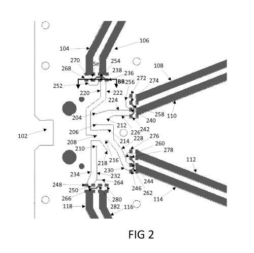
[0032] FIG. 2 depicts a blown up view of another embodiment of the
connection portion 102.
The connection portion 102 includes vias 204, 206, 208, 210, 212, 214, 216,
and 218 that are
sized to engage the pins of a high speed communication jack. Pin traces 220,
222, 224, 226, 228
230, 232 and 234 extend radially from the vias 204, 206, 208, 210, 212, 214,
216, and 218
towards the traces 104, 106, 108, 110, 112, 114, 116 and 118. Each pin trace
220, 222, 224, 226,
228, 230, 232 and 234 extends to an end point 236, 238, 240, 242, 244, 246,
248 and 250. Each
pin trace 220, 222, 224, 226, 228, 230, 232 and 234 is also matched to an
adjacent pin trace 220,
222, 224, 226, 228, 230, 232 and 234. As an illustrative example, pin trace
220 is matched to pin
trace 222, pin trace 224 is match with pin trace 226, pin trace 228 is matched
to pin trace 230 and
pin trace 232 is matched to pin trace 234. Each pin trace 220, 222, 224, 226,
228, 230, 232 and
234 has a length (L), a height (H) and a width (W), and is separated from an
adjacent pin trace by
a distance (S). The width of each pin trace 220, 222, 224, 226, 228 230, 232
and 234 is
approximately 35 mils. By adjusting the length, height and width of adjacent
pin traces, the
inductance of adjacent pin traces can be matched to each other. The end point
236, 238, 240,
242, 244, 246, 248 or 250 of each pin trace is separated from a respective
trace 102, 104, 106,
108, 110, 112 or 114 by a predetermined distance (Se).
[0033] End traces 252, 254, 256, 258, 260, 262, 264 and 266 extend from a
respective end
point 236, 238, 240, 242, 244, 246, 248 or 250 of a pin trace 220, 222, 224,
226, 228 230, 232
and 234 to a termination point 268, 270, 272, 274, 276, 278, 280 or 282. The
end traces 252,
6
CA 02942149 2016-09-02
WO 2015/148388 PCT/US2015/022032
254, 256, 258, 260, 262, 264 and 266 may also extend from the side of the pin
trace 220, 222,
224, 226, 228 230, 232 and 234 to the termination point 268, 270, 272, 274,
276, 278, 280 or
282. The termination points 268, 270, 272, 274, 276, 278, 280 or 282 are
separated from the
ends of each respective trace 102, 104, 106, 108, 110, 112 or 114 by the
predetermined distance
Se. In one embodiment, the distance Se, is constant along the length of the
end trace 252, 254,
256, 258, 260, 262, 264 and 266. In another embodiment, the distance Se,
varies along the
length of the end trace 252, 254, 256, 258, 260, 262, 264 and 266. Each end
trace 252, 254, 256,
258, 260, 262, 264 and 266 has a length (L), width (W) and height (H). By
adjusting the length,
height and width of each end trace 252, 254, 256, 258, 260, 262, 264 and 266
in conjunction with
the separation distance Se, different inductive and conductive configurations
can be achieved. .
The width of each branch trace 234, 236, 238 and 240 may be approximately 35
mils. The width
of each end trace 252, 254, 256, 258, 260, 262, 264 and 266 may be
approximately 10 mils.
[0034] FIG. 3 depicts a cut away view of the connection portion 102. The
connection portion
102 includes a top surface 302. The end points 236 and 238 and the termination
points 268 and
270 are positioned on the top surface 304 such that the end points 236 and 238
and termination
points 268 and 270 alternate across the surface 304 of the substrate. A first
grounding trace 306
and a second grounding trace 308 are positioned in the dielectric layers below
the top surface
with the first grounding trace 306 being separated from the top surface 302 by
a first dielectric
layer having a height Hi. The second grounding trace 308 is separated from the
first grounding
trace 306 by a second dielectric layer 310 having a second height H2. By
adjusting the heights
H1 and H2 of the dielectric layers 308 and 310, the capacitance of each trace,
end point, and
termination point can be adjusted. Further, the impedance of each trace 252,
254, 256, 258, 260,
262, 264 and 266, pin trace 220, 222, 224, 226, 228 230, 232 and 234, end
point 236, 238, 240,
7
CA 02942149 2016-09-02
WO 2015/148388 PCT/US2015/022032
242, 244, 246, 248 or 250 and termination point 268, 270, 272, 274, 276, 278,
280 or 282 can be
adjusted by modifying the length, width and height of each respectively. By
adjusting the
impedance of adjacent traces, end points and termination points the adjacent
traces and points
can be magnetically coupled to one another eliminating crosstalk or noise. The
dielectric layers
are made from a material having a dielectric constant greater than 3.0 such
as, but not limited to,
RO XT8100, ROGERS Material, or any other material capable of isolating a high
frequency
electrical signal.
[0035] FIG. 4 depicts a diagram of the circuit formed in the testing unit
100 in FIG. 2. The
schematic includes the connection portion 402, an input stimulus 404, a RJ 45
high speed
communication jack 406 and a output load 408. The RJ 45 jack 406 includes
internal traces 410
and 412 that are connected to pins 416 and 418 which engage vias 422 and 424.
The vias 422
and 424 are electrically connected to the pin traces 424 and 426 on the
testing unit 100. The
length, width, height and separation distance of the end traces 252, 254, 256,
258, 260, 262, 264
and 266 and pin traces 220, 222, 224, 226, 228, 230, 232 and 234 are adjusted
to create
difference capacitance values along the length of the traces 102, 104, 106,
108, 110, 112 or 114.
The inductance of each pin trace is changed by adjusting the height H1 of the
dielectric layer
under the pin traces 220, 222, 224, 226, 228, 230, 232 or 234 and the height
H2 between the
second grounding trace 306 and first grounding trace 304 under each pin trace
220, 222, 224,
226, 228, 230, 232 and 234. The capacitors created by the pin traces 220, 222,
224, 226, 228,
and the grounding traces 304 and 306 are sized between approximately 1
picofarads (pF) to
approximately 5pF. The top and bottom surfaces of the unit 100 may be covered
in a plastic
insulating layer to further enhance the operation of the circuit.
8
CA 02942149 2016-09-02
WO 2015/148388 PCT/US2015/022032
[0036] The capacitors created by the traces 102, 104, 106, 108, 110, 112 or
114 and the
grounding traces 304 and 306 are sized between approximately 0.5 lpF to
approximately 2pF.
The top and bottom surfaces of the unit 100 may be covered in a plastic
insulating layer to
further enhance the operation of the circuit. In one embodiment, signals are
driven through the
line using between approximately 4mW of power and 20mW of power.
[0037] FIG. 5 depicts one embodiment of a testing unit for a high speed
communication jack.
The testing unit 500 includes a high speed communication jack 502 connected to
the connection
portion 102 of the testing unit may be a RJ type connector, Universal Serial
Bus (USB)
connector and jack, Fire-wire (1394) connector and jack, HDMI (High-Definition
Multimedia
Interface) connector and jack, D-subminiature type connector and jack, ribbon
type connector or
jack, or any other connector or jack receiving a high speed communication
signal. The high
speed communication jack 502 is connected to the connection portion 102 such
that each pin on
the high speed communication jack 502 corresponds to one of the vias 202, 204,
206, 208, 210,
212, 214 and 216. The high speed communications jack 502 may be configured
such that pairs
of pins are magnetically coupled together.
[0038] Each trace 104, 106, 108, 110, 112, 114, 116 and 118 extends from
the connection
portion 102 to the connection units 120, 122, 124, 126, 128, 130, 132 and 134.
The connection
units 120, 122, 124, 126, 128, 130, 132 and 134 are configured such that a
cable having a
connector, such as an RJ 45 connector, can be removably attached to each of
the connection units
120, 122, 124, 126, 128, 130, 132 and 134. The connection units 120, 122, 124,
126, 128, 130,
132 and 134 transmit signals from the cable connected to the connection unit
120, 122, 124, 126,
128, 130, 132 and 134 and the associated trace 104, 106, 108, 110, 112, 114,
116 or 118
connected to the connection unit 104, 106, 108, 110, 112, 114, 116 and 118.
The connection
9
CA 02942149 2016-09-02
WO 2015/148388 PCT/US2015/022032
units 104, 106, 108, 110, 112, 114, 116 and 118 are affixed to a connection
plate 504 that extends
around the periphery of the testing unit 500. The connection plate 504 may be
made of metal,
such as steel, or metallized plastic. Each of the connection units 104, 106,
108, 110, 112, 114,
116 and 118 are affixed to the side surface of the connection plate 504 such
that the central axis
of the connection unit 104, 106, 108, 110, 112, 114, 116 or 118 is
substantially parallel to the
surface of the testing unit 500.
[0039] FIG 6 depicts a schematic representation of multiple testing units
connected together
across a network. A first testing unit 602 is connected to a second testing
unit 604 by a cable 606
connected to the high speed communication jack on each of the testing unit 602
and 604. The
cable 606 may be a communication cable such as an Ethernet cable, a category
5, 6, or 7 cable, a
serial cable, a Fire-wire cable, a USB cable or any other type of
communication cable. The cable
606 includes connectors (not shown) to allow the cable 606 to be removably
connected to the
high speed communication jacks. In one embodiment, the high speed
communication jack on the
first testing unit 602 is the same type of high speed communication jack as
the second testing
unit 604. In another embodiment, the high speed communication jack on the
first testing unit
602 is a different type than the high speed communication jack on the second
testing unit 604.
The cable can be of any length including, but not limited to, 3 feet, 6, feet,
10 feet, 12 feet, 15
feet or 20 feet.
[0040] The connection units 104, 106, 108, 110, 112, 114, 116 or 118 each
connect to a
signal transmission and receiving unit 610 and 612 via cables coupled to the
connection units
104, 106, 108, 110, 112, 114, 116 or 118 on one end and to the signal
transmission and receiving
units 610 and 612 on the opposite end. In one embodiment, the signal
transmission and
receiving unit 610 transmits a signal from the first testing unit 602 to the
second testing unit 604
CA 02942149 2016-09-02
WO 2015/148388 PCT/US2015/022032
via the high speed connection jacks on the first and second testing units 602
and 604. Upon
receiving the signal, the second testing unit 604 transmits the signal to the
signal transmission
and receiving unit 612. In one embodiment, the signal transmission and
receiving unit 612
transmits a new signal back to the signal transmission and receiving unit 610
over the cable 608.
In one embodiment, the signal transmission and receiving unit 612 transmits a
second signal to
the signal transmission and receiving unit 612 that is based on the signal
previously transmitted
by the signal transmission and receiving unit 610. In another embodiment, the
signal
transmission and receiving unit 612 transmits a second signal to the signal
transmission and
receiving unit 610 that is substantially identical to the signal previously
transmitted by the signal
transmission and receiving unit 610.
[0041] The preceding detailed description is merely some examples and
embodiments of the
present disclosure and that numerous changes to the disclose embodiments can
be made in
accordance with the disclosure herein without departing from its spirit or
scope. The preceding
description, therefore, is not meant to limit the scope of the disclosure but
to provide sufficient
disclosure to one of ordinary skill in the art to practice the invention with
undue burden.
11