Note: Descriptions are shown in the official language in which they were submitted.
CA 02943565 2016-09-22
WO 2014/146195
PCT/CA2014/000279
ELECTRONIC SINE WAVE TRANSFORMER
FIELD OF THE INVENTION
[00011 The present invention relates generally to an electronic sine wave
transformer
circuit and more particularly to a circuit for transferring alternating
current (AC) power
from a source to a load using magnetic storage coupling.
BACKGROUND OF THE INVENTION
100021 Existing technologies that transfer power from a source to a load
utilize
converters that use capacitors as DC capacitive storage. Typically, DC
capacitive storage
systems have been used for size, and cost reasons. In such cases, the energy
is stored
within the capacitor as V2 CVA2. That is, generally speaking, the capacitor
stores energy
in the form of an electrical charge that produces a potential difference
across the
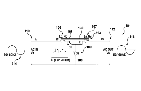
capacitor plates. One of the issues with such circuits is that they require
rectification,
direct wire connection, current pulses, DC regulator circuits for DC output,
inverters to
reproduce square wave outputs or more complex digital to analog power shapers
to re-
create AC sine waves and other such complexities. Additionally, such previous
electronic converter circuits using DC capacitive storage typically receive an
input
alternating current (AC) signal and are converted to direct current (DC) to
allow for the
energy storage within the capacitor thereby outputting a DC signal to a load.
This may
not always be desirable as in most power transfer cases an AC output signal is
desired
because a large percentage of power (work) equipment is required to operate
from AC
sine wave sources and the larger the loads, the more pure (without power
harmonic
content) the source power is required. Usually this is only possible with
direct line-load
connections.
[0003] That is, existing converters change the input voltage to DC, store the
energy in a
capacitor and then use switching systems to convert to the desired output
level. This
requires input current control to minimize harmonics, rectifiers, storage
capacitors, output
filters. These are relatively complex systems and do not normally provide a
clean
1
CA 02943565 2016-09-22
WO 2014/146195
PCT/CA2014/000279
sinusoidal output waveform (i.e. these systems have power harmonics and high
frequency
harmonics on the input and output).
[0004] It would be advantageous to provide a circuit for transferring power to
a load
from a source to transfer the energy such as to obviate or mitigate the
disadvantages of
capacitive storage solutions. Additionally, it would be advantageous to
provide a circuit
that allows an input AC to be output as an output DC signal without diode
rectification
and other associated re-construction steps.
SUMMARY OF THE INVENTION
[0005] According to one aspect, there is provided an electronic sine wave
transformer
circuit comprising an input node adapted to receive an input alternating
current (AC)
power source having an input voltage operating at an input frequency in a
Hertz range;
the magnetic storage coupling unit comprising: a first set of windings coupled
to a first
bi-directional AC switch, the first bi-directional AC switch for receiving an
input
charging current associated with the input voltage; a second set of windings
located in
series with the first set of windings, the first and second set of winding
sharing a common
core; a second hi-directional AC switch connected at one end between the first
and
second set of windings and at another end to a common ground, the first and
second bi-
directional AC switches having a switching frequency in a kilohertz range and
switching
between on and off in alternating modes; and an output node connected to the
second set
of windings, the output node adapted to provide an output AC power having a
frequency
of the input frequency, the output power having an output voltage with an
amplitude
based on the input voltage and at least one of: a winding ratio of the first
and second set
of windings, a polarity of the first and second set of windings and a duty
cycle of the first
and second bi-directional AC switches; wherein the magnetic storage unit is
configured
to receive said input power and transfer the input power between the input
node to an
output node such that the first set of windings and the second set of windings
are
configured to provide magnetic storage of energy based on each of the first
and the
second bi-directional AC switches being continuously switched.
2
CA 02943565 2016-09-22
WO 2014/146195
PCT/CA2014/000279
[0006] In some aspects, the input AC power and the output AC power can be a
sine
wave. In other aspects the circuit can further comprising a capacitor located
between the
second set of windings and the common ground, the capacitor configured to
suppress
high frequency components in the kilohertz range of the output signal at the
output node.
In yet other aspects, the output voltage signal can be further dependent upon
a turns ratio
of the first set of windings relative to the second set of windings such that
varying at least
one of the turns ratio and the duty cycle directly varies the output voltage
signal
amplitude. In still other aspects, the circuit can provide a predefined
constant ratio of
voltage transfer from the input node to the output node. In yet another
aspect, the circuit
can provide a near zero power harmonic distortion in both the input and output
power
where the switching frequency is greater than about 100 times the input
frequency. In yet
still further aspects, the circuit can provide a harmonic correction for non-
linear loads
incrementally varying the duty cycle to correct for the anticipated
fluctuations of said
non-linear loads.
[0007] In yet another aspect, the circuit can comprise a second capacitor
located between
the first bi-directional switch and the common ground, the second capacitor
configured to
suppress high frequency current components at the input node. In a related
aspect, the
circuit can further comprise an input inductor located between the input node
and the first
bi-directional switch and an input capacitor located between the input node
and the
common ground, the input inductor cooperating with the input capacitor to
provide
additional suppression of high frequency components at the input node. In a
further
aspect, the input and output powers, voltages and currents have limited
harmonic content
other than the base power Hertz frequency content and the kilohertz high
frequency
components generated by the switching frequency are limited.
[0008] In some aspects, there can be a first duration where the first bi-
directional AC
switch is on and the second bi-directional switch is off, a current is
permitted to flow
from the first and second sets of windings to the load, the first and second
sets of
windings being magnetically charged for the first duration that the first bi-
directional AC
switch is closed. In a further aspect, there can be a second duration where
the second bi-
directional AC switch is on and the first bi-directional switch is off, the
current ceases to
3
CA 02943565 2016-09-22
WO 2014/146195
PCT/CA2014/000279
flow at the first set of windings and the current at the load point is
maintained by the
second set of windings as it magnetically discharges. In still further aspect,
the magnetic
storage unit can be configured to maintain a constant output voltage ratio to
the supply
input voltage for the load during the switching operation of the first and the
second bi-
directional AC switch. In still a further aspect, the output voltage can be
varied
proportionally based on at least one of a turns ratio of the first set of
windings relative to
the second set of windings and the duty cycle.
[0009] In other aspects, the first and second switches can be operated at only
certain
durations of the Hertz frequency such that only a portion of the input voltage
waveform is
transferred to the load. In some aspects, the switching frequency of the first
and second
switches can be applied only during the positive phase or negative phase of
the input
voltage thus producing a positive or negative only controllable output voltage
without a
rectifier at the output node.
[0010] In yet other aspects, the input power source can be DC voltage and the
first and
second switches duty cycles are modulated at regular repeating Hertz rates
with duty
cycle variations so as to produce varying output voltages selected from:
linear sinusoid
voltages or non-linear outputs voltages to the load. In still other aspects,
feedback can be
used to control the duty cycle of the first and second hi-directional AC
switches to
provide a more stable output with respect to variations of input voltage.
BRIEF DESCRIPTION OF THE DRAWINGS
[0011] Embodiments of the present invention will now be described by way of
example
only with reference to the following drawings in which:
Figure 1A is a schematic drawing of an electronic sine wave transformer
circuit;
Figure 1B is a schematic drawing of an electronic sine wave transformer
circuit
according to another embodiment;
4
CA 02943565 2016-09-22
WO 2014/146195
PCT/CA2014/000279
Figure 1C is a schematic drawing of an electronic sine wave transformer
circuit
according to another embodiment;
Figure 10 is a schematic drawing of an electronic sine wave transformer
circuit
according to another embodiment;
Figure 1E is schematic drawing of an electronic sine wave transformer circuit
according to another embodiment;
Figure 2 is an illustration of the current waveform of the current through the
storage set of windings and a current waveform illustrating the average
current
through the storage set of windings;
Figure 3A is a block diagram of the electronic sine wave transformer circuit
of
Figures 1A-1E;
Figure 3B is a block diagram of the electronic sine wave transformer circuit
of
Figure 3A showing a half-wave rectification; and
Figure 3C is a block diagram of the electronic sine wave transformer circuit
of
Figure 3A showing an inverter to recreate an AC waveform using duty cycle
modulations.
DETAILED DESCRIPTION OF THE PREFERRED EMBODIMENT
[0012] For convenience, like numerals in the description refer to like
structures in the
drawings.
Referring to Figures 1A-1E generally, alternate circuit schematic
arrangements are shown, in accordance with different embodiments, for an
electronic
sine wave transformer (hereinafter ESWT) circuit that allows the conversion or
transfer
of power from a source node to a load using magnetic storage coupling and high
frequency pulses (provided by one or more switches) that are used to charge a
magnetic
CA 02943565 2016-09-22
WO 2014/146195
PCT/CA2014/000279
storage unit comprised of one magnetically coupled core with multiple
windings. That is,
the magnetic storage of energy is handled by one core with multiple sets of
windings that
are coupled together and connected to one or more switches that provide the
high
frequency pulses to control the charging and discharging of the core and the
sets of
windings in the magnetic storage unit. Further, the magnetic storage coupling
unit causes
an input AC power and voltage to be transferred to the output (e.g. to a load)
at a same
operating frequency as the input power and voltage while using magnetic energy
storage
via a central storage core and a coupled number of sets of windings that are
controlled by
one or more switches.
[0013] Specifically, an input AC power supply provides an input supply voltage
at a base
frequency in a hertz range (e.g. under 400 Hz for typical line frequency) to a
magnetic
storage coupling unit. The magnetic storage coupling unit as will be
described, is
implemented in the form of a common core with one or more sets of windings and
at
least two bi-directional AC switches (e.g. a first and a second bidirectional
switch) that
are alternately turned on and off and supply high frequency magnetic pulses to
the
common core windings (shown having inductance Lc, Ld) and to the load. At
least one
of the switches is coupled to a first one of the sets of windings in series,
while another
one of the switches is coupled between the sets of windings and a common
ground.
Further, the first and second switch are switched in opposite modes (i.e. the
first switch is
on and the second switch is off, and vice versa) and the switching frequency
is at much
larger frequency (e.g. in a kilohertz range) than the base frequency of the
input power
supply (e.g. in a hertz range). In this manner, the first and second sets of
windings (e.g.
taken in combination) only see short charging pulses and also short
discharging pulses
between charging pulses.
[0014] That is, in one mode where the first switch is on (and the second
switch is off),
both the first and second sets of windings collectively get charged and store
energy
therein. In this case, the current flows through both the sets of windings and
the total
energy or magnetic flux stored is: E=1/2 LIA2. Where L refers to the
inductance of the
first and second sets of windings taken together and I is the magnetic
charging current
flowing therethrough.
6
CA 02943565 2016-09-22
WO 2014/146195
PCT/CA2014/000279
100151 In a second mode where the second switch is on (and the first switch is
off), now
the total current flows through only the second set of windings and thus the
current is
increased in order to maintain the magnetic flux at the start of the discharge
pulse and
then slowly decreases as energy is used to support load power. At an open
circuit load
condition, the charge current is in one polarity and the discharge current
goes thru zero
current and in the opposite direction so as to maintain a constant ratio of
output voltage to
input. That is, the output wave shape follows the sine wave input wave shape
but the
current alternates between one direction and the other to maintain zero net
current flow.
100161 Further, the magnetic storage coupling unit, allows the output voltage
provided to
the load to directly follow the shape of the input supply voltage. That is, if
the input
supply voltage is a sine wave with a particular base frequency, the output
voltage
supplied to the load is a sine wave with the same base frequency and a direct
copy of the
wave shape but at a proportional amplitude difference according to the ratio
of the
windings and the duty cycle of the electronic switches. The amplitude of the
output
voltage supplied to the load is a function of a voltage constant Kv and the
input voltage
supply amplitude. The relation is valid at the kilohertz frequency which is
essentially
instantaneous at the power hertz frequency of the input power and by extension
is valid
for the complete sine wave or any portion thereof, including truncating or re-
starting of
the switching at any part of the sine wave. The voltage constant Kv is further
dependent
on the turns ratio (a measure of the ratio of the number of turns of the sets
of windings
relative to one another) and the duty cycle. That is, since the turns ratio is
fixed, the
output voltage can be controlled by the duty cycle of the switching frequency
of the first
and second switches. Therefore, the voltage change between the input and
output
happens at the magnetic storage unit. The net result is that energy is stored
at the set of
windings and discharged to the load within the normal storage law of 1/2 LIA2.
This means
that the charge current slope is controlled by the charge voltage and Lc+Ld
and the
discharge slope is controlled by the output voltage and Ld only.
[0017] The end function of the ESWT is the somewhat the same as a conventional
magnetic power transformer with an input winding and an output winding. As
will be
understood with reference to Figures 1A-1E for example, one of the differences
of the
7
CA 02943565 2016-09-22
WO 2014/146195
PCT/CA2014/000279
ESWT circuit presented herein to existing transformer circuits is that in
known
transformer circuits having windings without the use of switching as proposed
herein, the
full voltage and current for each half cycle needs to be supported inductively
by the
transformer, this commonly referred to as the magnetizing inductance.
Conversely, in the
ESWT circuit discussed herein, the inductance (e.g. first and second sets of
windings
located in series) are charged for short pulses at a time (during the high
switching
frequency) and similarly discharge magnetically for short pulses.
Additionally, in terms
of size, existing transformer circuits can have a typical weight of around 100
lbs to
accommodate the large magnetizing inductance, whereas the ESWT circuit
presented
herein has a significantly smaller size (e.g. 1 lb) and can be operated with a
full sine wave
input or any part of a sine or any other voltage source AC or DC.
[0018] In accordance with Figures 1A-1E, the ESWT circuit uses magnetic
storage and is
inherently hi-polar. That is, the energy can be stored in both polarities
without any
changes. Also, it can be transferred to the load in a half wave form. This is
not possible
with conventional transformers.
[0019] Further to expand on the advantages presented with the electronic sine
wave
transformer of Figures 1A-1E, A conventional transformer can be represented
with an
input leakage inductance, mutual inductance and output leakage inductance. All
with the
appropriate turns ratio applied. That is, the mutual inductance of the sets of
windings in
the circuit is the controlling element. At maximum working voltage the core
flux is
below saturation (i.e. typically 15 kGauss). The ampere-turns resulting from
the applied
voltage (at 50/60/400 Hertz) is such that the flux created by the volt-sec
(area under one
half sine) divided by the core area is less than saturation point of the core
material. A
typical multi-KVA transformer measures at 1 Henry with a weight of approx. 50-
100 lb.
with an included motorized control to allow variability. Preferably, the ESWT
circuit of
Figures 1A-1E charges and discharges the magnetic flux storage element with
only
sufficient flux to cover one high frequency cycle (kilohertz) to ferrite
saturation levels
that are typically 3 kGauss. In a preferred embodiment, the voltage transfer
ratio works
for sine waves and non-sinusoidal waveforms. Further preferably, the magnetic
storage
unit 100 presented in Figures 1A-1E weighs only 1 lb. Therefore there is
material saving,
8
CA 02943565 2016-09-22
WO 2014/146195
PCT/CA2014/000279
cost and increased flexibility. The instantaneous and electronically variable
nature of the
transformer circuit of Figures 1A-1E allows control without any mechanical
wear items.
[0020] As mentioned, the first and second switches of the magnetic storage
unit have a
switching frequency that can be orders of magnitude greater than the input
frequency of
the input power source. For example, preferably the switching frequency is in
the kHz
range and typically greater than 100 times the base power frequency which is
in the hertz
range. That is, there are no harmonics below the kHz range switching
frequency. In this
manner, power harmonics of the output power, provided at the output of the
magnetic
circuit that is being supplied to the load is minimized and for all practical
purposes the
power harmonics are eliminated. Additionally, the inductance sizes in the
magnetic
circuit and any capacitors used in the electronic sine wave transformer
circuit for
suppressing high frequencies above the hertz range are minimized.
[0021] It is further noted, that according to Figures 1A-1E, the electronic
sine wave
transformer circuit presented in Figures 1A-1E, receives an AC sine wave power
and
voltage at the input source at a first frequency and provides an AC sinewave
power and
voltage curve having the same shape as the input curve (e.g at the first
frequency) with a
magnitude or amplitude of the output AC sinewave power and voltage being
controlled
by the fixed turns ratio of the sets of windings and the variable electronic
timing of the
switches in the magnetic storage unit (e.g. considering that the ratio of the
turns of the
first and second windings are kept constant). This is advantageous, as the
ESWT circuit
presented in Figures 1A-1E allows for the output power/voltage to be
controlled
electronically rather than using variable taps or motorized variable
transformers. The
circuit also provides a further advantage in that it allows controlling the
output energy by
storing it in the inductance of the windings (e.g. as magnetic charge) rather
than
capacitive storage which would require rectification and other such
complexities. In
addition because, the input power is an AC signal (e.g. sinewave) and the
output power is
an AC signal (e.g. sinewave of same frequency and shape as input signal) then
the size,
weight and conversion losses (e.g. due to conversion of the signal to DC and
back to AC
in existing DC capacitive storage system) is significantly reduced. This is an
advantage
not only over the conventional power transformer but also over capacitive
storage
9
CA 02943565 2016-09-22
WO 2014/146195
PCT/CA2014/000279
switching power controllers.
[0022] Referring now to Figures 1A-1E, shown are exemplary embodiments of an
electronic sine wave transformer circuit illustrated generally by reference
numerals 101-
105 according to alternate embodiments.
[0023] Referring to Figure 1A, shown is the electronic sine wave transformer
circuit
101. The electronic sine wave transformer circuit 101 comprises an input node
110, an
output node 112 and a magnetic storage unit 100 coupled electrically between
the input
node 110 and the output node 112 connected to a load. The input node 110 is
located at
the source side for receiving an input AC (alternating current) power source
having an
input supply voltage 114 which operates at a low base frequency (e.g. at a
line frequency,
typically below 400 Hz). The magnetic storage unit 100 then serves to
transform or
transfer power from the source side to the load using high frequency magnetic
energy
storage. Magnetic storage unit 100 comprises a common core 130 having one or
more
sets of windings (e.g. a first set of windings 106 and a second set of
windings 107) for
storing energy magnetically within common core 130 (referred to as storage
node 113).
The magnetic storage unit 100 further comprises two or more switches (e.g. a
first switch
108 and a second switch 109). The first and second switches 108-109 are AC
bidirectional switches, illustrated generally at 140, that are switched on,
alternately, that
is opposite to one another and have a switching frequency in a kilohertz range
(e.g.
preferably orders of magnitude larger than the input power frequency).
[0024] Referring to the magnetic storage unit 100, the first set of windings
106 and
second set of windings 107 are magnetically coupled together by common core
130.
Preferably, the second set of windings 107 is located in series aiding or
series opposing
connection with the first set of windings 106 within a common magnetic path.
Additionally, the first switch 108 is directly connected to the first set of
windings 106
(and can be located on either side of first set of windings 106 as illustrated
in the
difference between FIGS. 1A and 1C).The second switch 109 is connected between
the
two set of windings 106, 107 and the common ground. The output node 112 is
then
connected to the second set of windings 107 such that the output node provides
an output
CA 02943565 2016-09-22
WO 2014/146195
PCT/CA2014/000279
AC power having a frequency of the input base power frequency to the load, and
an
output voltage 116 operating at the base frequency. Further the amplitude or
magnitude
of the output voltage 116 is based on one or more of: a winding ratio between
first and
second sets of windings 106,107, a polarity of the first and second set of
windings 106,
107 and the duty cycle of the switching frequency of the first and second
switches 108,
109. As will be described, the magnetic storage unit 100 is configured to
receive the
input power and transfer it to the output node 112 such that the first and
second set of
windings 106, 107 provide magnetic storage of energy in a continuous fashion
therein
even while the first and second switches 108 and 109 are being alternately and
in an
opposing manner being switched on and off.
[0025] In one example, referring to Figure 1A and the magnetic storage unit
100, the
switch 108 and 109 duty cycle is set at a predefined number the set of
windings 106, 107
are coupled together and each have a predefined number of windings. Referring
to
Figure 1A, Nd refers to the number of windings to produce the inductance Ld of
second
set of windings 107, and Nc refers to the additional turns to produce the
inductance Lc
(referring to the combination of the first and second set of windings 106,
107). That is,
Nc+Nd produces the inductance Lc+Ld. The inductance is proportional to the
number of
turns squared.
[0026] The following describes the general mode of operation of the magnetic
storage
unit referred to in each of Figures 1A-1E. In the first mode of operation,
when the first
switch 108 is switched on (and second switch 109 is switched off), the line
current flows
through the first and second sets of windings 106, 107 (storage node 113) to
the load at
output node 112. In this manner, the output current lo is equivalent to the
input current Is
which is equivalent to the current flowing through the set of windings Ic and
Id. In this
manner, the current flowing through the sets of windings 106, 107 supports the
load
current (To) plus the magnetic charging current. That is, the combination of
both sets of
windings 106, 107 (storage node 113) preferably supports the desired peak
output current
To plus the peak charging current and the current flowing through the second
set of
windings 107 similarly must support the peak limits of the discharge current.
That is, the
magnetic energy flux (known as BH) load of the common core 130 of storage node
113
11
CA 02943565 2016-09-22
WO 2014/146195
PCT/CA2014/000279
preferably does not reach saturation with the peak ampere-turns mentioned
above.
[0027] Referring again to Figures 1A-1E, the input supply voltage 114, is
preferably an
AC sine wave operating at a base frequency (e.g. 50, 60 or 400 Hz), and the
output
voltage 116 at output node 112 is also an AC sine wave operating at the same
base
frequency (e.g. 50, 60 or 400 Hz). Preferably, referring to Figures 1A-1E, the
switching
frequency of switches within the magnetic storage unit 100 (e.g. the first
switch 108 and
the second switch 109) is much higher than the base frequency and in the
kilohertz range
(e.g. 20kHz) while the base frequency is in the Hertz range (e.g. below 400
Hz). That is,
as will be described, the magnetic storage unit 100, facilitates transforming
a power AC
voltage input to a power AC voltage output at the load by transforming or
transferring the
input energy using magnetic energy storage as the transfer medium.
[0028] Referring again to the first mode of operation, when the first switch
108 is
switched on, the current flows through the first and second sets of windings
106, 107
(which are in series in this mode) to the load.
[0029] Generally speaking , the instantaneous output voltage at node 112, is
defined as:
VC
K õVs = ¨7
and the output current at node 112 is 'I,
where Kv is a predefined constant
that is dependent on the turns ratio between the first and second sets of
windings 106, 107
(e.g. specifically on the number of turns Nc of the first set of windings 106
relative to the
number of turns Nd of the second set of windings 107). That is, Kv is a
function of the
turns constant and the charge/ discharge ratio as
defined below. Further, the
charge/discharge ratio is dependent upon delta-tc, the time to switch from the
first switch
108 being switched on to the second switch 109 being switched on and delta-td
which is
the discharge time when the second switch 109 is on (first switch 108 is off).
[0030] This can be further understood as:
At, 1
Kv = ICK Atd ¨
, ____________________ ¨ ____ , constant for ratio of Vo to
+1
[0031] Kx
12
CA 02943565 2016-09-22
WO 2014/146195
PCT/CA2014/000279
At
Kx= ¨
[0032] Where Atd and
K,=(11,,Ard , constant for ratio of r(avg) to Id(avg)
[0033] c +Nd
=
[0034] As seen by the instantaneous values of the output voltage 116, a
constant duty
cycle will yield a constant output voltage 116 relative to the input voltage
114 and
thereby transform an input sinewave to an output sinewave.
[0035] Referring now to the current waveform of Figure 2 illustrating the
current through
the storage node 113. Further, in the first mode, the current flowing through
the storage
node 113 increases from Icl to Ich while the first switch 108 is on and the
second switch
109 is turned off. The current increase can be shown as follows:
/c/(N, + Nd) = /diNd Icz = 41( __ Nd )= irdikrz
[0036] Nc+
)
I
Nd Nd ¨ K K ¨ (Ar c-FI
VZ
Ich(Nc-I-Wd)= ldhNd ich= latc+Nct ¨ dh z ¨
[0037]
[0038]
=th¨ii= (1dh-1,11)KI, =
e
[0039] Subsequently, in the second mode, the first switch 108 is switched off
and the
second switch 107 is switched on, now all the current flows through the second
set of
windings 107 only, and the current instantly increases from Ich to Idh to
maintain the
conservation of energy in the magnetic field. That is, the current magnitude
increases by
the turns ratio difference. For example, in a scenario where Nc of set of
windings 106 is
equivalent to Nd of set of windings 107 then the current flowing through the
second set
of windings 107 increases to Idh (e.g. doubles in value compared to the
current just
before switch 108 is turned off in this case). Subsequently, during the
following pre-
defined discharge time interval while the second switch 107 is conducting ,
the current
through the storage node 113 slowly decreases from Idh to Idl, the relation
being shown
above. Further, the current instantly decreases at the end of the discharge
time interval
when the second switch 109 is turned off and the first switch 108 is turned
back on, from
13
CA 02943565 2016-09-22
WO 2014/146195
PCT/CA2014/000279
Idl to Icl.
[0040] As can be seen, a constant flux is maintained even during the time that
each
switch 108, 109 is turned on/off and during the transitions between modes.
That is, the
magnetic field and energy stored within the magnetic storage node 113 is kept
constant
during the switching modes from charge/discharge/charge.
[0041] The continuous storage of energy described in reference to the magnetic
storage
unit 100 of Figures 1A-1E refers to the fact that during the first and second
mode of
operations and switching therebetween (e.g. switching from the first switch
108 being
turned on to the second switch 109 being turned on), the input-output voltage
ratios (114
and 116) are maintained as the magnetic field and the energy stored within the
storage
node 113 remains constant as defined by E=1/2LIA2. That is, in a preferred
embodiment,
a constant ratio of voltage transfer from the source side to the load side is
maintained
irrespective of the input sine wave shape (e.g. input supply voltage 114) and
the input
sine wave shape of voltage 114 is converted at the fixed transfer ratio (e.g.
determined as
mentioned earlier by the Kv constant) to the load side as output voltage 116.
The load
impedance will thus determine the output current.
[0042] The mathematical relationships of voltages and currents used in Figures
1A-1E
can be further understood as follows:
V
[0043] During the charge and discharge times, V' 3 and remain essentially
unchanged
because the switching frequency is much greater than the line frequency
(typically 20kHz
switching vs 60 Hz line). Therefore, the voltage and inductance of one of the
sets of
windings is given by:
At
V = L¨ L = ALIO , AL, = -magnetic core inductance factor, N = &umber of turns
t
[0044] = instanteneous value of the 60 Hz input sine wave
[0045] V0= instanteneous value of the 60 Hz output sine wave
Atd
Al --Ti ________
O
[0046] ALNd2
14
CA 02943565 2016-09-22
WO 2014/146195
PCT/CA2014/000279
At,
[0047] MC = (Vs ¨ V0)ALOY,+Nd)2
V, Ata
= !Clad = K, ALN2
[0048]
At, V0Ltd
) ____________________
(Vs v ot
+ NO2¨ K ALAra
[0049]
At, ALNõ? At, 2 At,
(Vs Ves) = (Vs ¨ VO¨Litd Kt = K,V0 __________ K= ?K
[0050] ALM+ Ald)2 Atd
[0051]
[0052] V (1+ Kx)= KxVs
Kx1 1
Vo =I + K xVs = ______ iVs KvV5 Kv ¨ ____
iTx +1
[0053]
[0054] Note that Kv is a only a function of the turns constant IC, and the
duty cycle Kx
Ata Atd ,
d
= V ___________ 2 = Kv V, s 2 = õ. I) Vs 'd= K 2 , JAIrc = Aid Ki Ke
KdV5
[0055] ALNd J41,1\1,1 ALIVd
[0056] Note that the current ripple magnitude in the storage element 113 is a
function of
, the inductance values and the duty cycle.
[0057] The constants are:
K, = ____________ , constant for ratio of fc(avg) to Id(avg)
[0058] c+ Nd
At, +Atd
K0 = IC,Ato 4- Atd constant for ratio of lo to I (av.g),Td(avg)
[0059]
K ¨ KE
[0060] x Atd
CA 02943565 2016-09-22
WO 2014/146195 PCT/CA2014/000279
Atc
K
= K K = constant for ratio of Vo to V, 2' ` ,At, + Atd 1
IT, +1
[0061]
KvAtd
2 ; constant for ratio of ripple Alc,Ala
[0062] ALNd
[0063] The following are the simplified working relations:
[0064] V = KI'Vs
[0065] Aid = KrzVs
[0066] /1/, = ICKdVs
V.
= ¨
[0067] Z1
[0068] Id (a") =
100691 ic(avg) = KK0I0
At,
D = At, + At
duty cycle
[0070]
[0071] = D Ic(avg)= DK,K010.
At, Mc+ Ata
DKiK, = ______________________ = K.
[0072] Atc + Atd ICLAtc+ Atd
1
Kis=KvVoKvio = VoIc
[0073]
[0074] Further, the values for currents flowing through the transformer
circuits of 101-
105 can be calculated as follows:
16
CA 02943565 2016-09-22
WO 2014/146195
PCT/CA2014/000279
lch+ ldh Id
[0075] 7
Ic(aV 9 = 2 = 2 = idovg
[00761 Alc
= 1ch I 1 = (idh¨ Idl)10 =
lc(av,g)At,-F ld(avg)Litd Kild(avg)Ato -F Id(avg)Atd = Id(avg)K,Ato+ Atd
= __________________________
[0077] + Ltd A t, Lt a A tc+
Ata
At, + At,/
(avg) = K0.10 Ko= KiAto+Ata
[0078]
(a
[0079] Note that I c ro) 1 (avg e)
are a function of the load current, duty cycle and the
number of turns of the storage set of windings.
= ¨ = load impedance
[0080]
[0081] It is noted that the operation of the magnetic storage unit 100
described in
reference to Figure lA applies similarly to Figures 1B-1E.
[0082] In one embodiment referring to Figure 1B and 1C, shown is an electronic
sine
wave transformer 102, 103 according to alternate embodiments where an input
capacitor
117 located between the first switch 108 and/or the first set of windings 106
and the
common ground. The input capacitor 117 is configured for cooperating with both
the
first and second sets of windings 106, 107 to suppress the high frequency
current
components in the kilohertz range from the input supply side of the ESWT
circuit 102,
103 respectively. Further, there is provided an output capacitor 118, located
between the
second set of windings 107 and the common ground (e.g. across the load), the
output
capacitor 118 configured for cooperating with the first and second sets of
windings 106,
107 to suppress the high frequency components in the kilohertz range (e.g.
generated by
the high frequency switching rate of the first and second switches 108, 109)
of the output
power/voltage at the output node.
[0083] In yet another embodiment referring to Figure 1D, there is provided an
input
inductor 119 located between the input node and the first switch 108 and a
filtering
17
CA 02943565 2016-09-22
WO 2014/146195
PCT/CA2014/000279
capacitor 120 located between the input node and the common ground. The input
inductor 119 cooperating with the input capacitor 120 to provide additional
suppression
of high frequency components from the input signal (e.g. 114) provided to the
magnetic
storage unit 100. Figure 1E provides some exemplary values for the components
to filter
the appropriate frequencies in a line frequency embodiment.
[0084] In a preferred embodiment of Figures 1A-1E, the input and output
powers,
voltages and currents have no harmonic content other than the base input
frequency
(Hertz frequency) content, including the absence of the kilohertz high
frequency
component.
[0085] In yet another embodiment (not illustrated), the first and second
switches 108,
109) are operated at only certain portions of input waveform of the input
supply voltage
114 such that only a portion of the input voltage 114 waveform is transferred
to the load
as output voltage 116.
[0086] In yet another embodiment, the switching frequency of the first and
second
switches 108, 109 is only applied during the positive phase or negative phase
of the input
voltage thus producing a positive or negative only controllable output voltage
commonly
referred to as half wave rectification, without the use a diode or rectifier
at the output.
For example, in Figure 3B, first and second switches 108, 109 can be operated
in the
positive half-cycle of the input voltage 114 waveform to provide only the
positive
waveform 302 to the output node 112.
[0087] In yet another embodiment illustrated in Figure 3C, the input power
source (e.g.
114) can be a DC voltage and the switches 108, 109 duty cycles are modulated
at regular
repeating variations so as to produce varying output voltages 116 which are
selected from
linear sinusoid voltages or non-linear output voltages to the load.
[0088] In yet another aspect of the ESWT 101-105 of Figures 1A-1E, it is noted
that the
ripple currents (shown as delta Ic) are not affected by the load current Jo.
That is, when
the load is disconnected such as to cause a zero load current, there will only
be the ripple
current component above and below zero at the high frequency. The output
voltage 116
18
CA 02943565 2016-09-22
WO 2014/146195
PCT/CA2014/000279
will still be defined by the ratio to the input voltage 114 defined above.
[0089] In some embodiments, a feedback circuit can be used to monitor output
waveform
116 that is used to alter the duty cycle of the switches 108,109 to provide a
more stable
output voltage with respect to the input voltage.
[0090] Accordingly, it will be appreciated by a person of ordinary skill in
the art that the
present invention provides improved flexibility for the electronic sine wave
transformer
circuits by allowing electronic timing switching controls of the output
voltage provided to
a load and allowing an AC input power to be supplied as an output AC power
such that
the amplitude is dependent upon the turns ratio between the sets of windings
and the duty
cycle of the switches used in the magnetic storage unit 100 described herein.
Therefore
there is material saving, cost and increased flexibility. The electronics
variable nature of
the transformer circuit 101-105 allows control of output voltage, power and
current
without any mechanical wear items.
[0091] Further, although the invention has been described with reference to
certain
specific embodiments, various modifications thereof will be apparent to those
skilled in
the art without departing from the scope of the invention as defined by the
appended
claims.
19