Note: Descriptions are shown in the official language in which they were submitted.
CA 02943822 2016-09-23
[DESCRIPTION]
[Invention Title]
APPARATUS FOR TRANSMITTING BROADCAST SIGNALS, APPARATUS FOR RECEIVING
BROADCAST
SIGNALS, METHOD FOR TRANSMITTING BROADCAST SIGNALS AND METHOD FOR RECEIVING
BROADCAST SIGNALS
[Technical Field]
[1] The present invention relates to an apparatus for transmitting
broadcast signals, an
apparatus for receiving broadcast signals and methods for transmitting and
receiving broadcast
signals.
[Background Art]
[21 As analog broadcast signal transmission comes to an end, various
technologies for
transmitting/receiving digital broadcast signals are being developed. A
digital broadcast signal may
include a larger amount of video/audio data than an analog broadcast signal
and further include various
types of additional data in addition to the video/audio data.
[Disclosure]
[Technical Problem]
[31 That is, a digital broadcast system can provide HD (high definition)
images, multi-channel
audio and various additional services. However, data transmission efficiency
for transmission of large
amounts of data, robustness of transmission/reception networks and network
flexibility in consideration
of mobile reception equipment need to be improved for digital broadcast.
[Technical Solution]
141 To achieve the object and other advantages and in accordance with the
purpose of the
invention, as embodied and broadly described herein, a method for transmitting
a broadcast signal, the
method comprising: encoding service data corresponding to a plurality of
physical paths; time
interleaving the encoded service data in each physical path by time
interleaving (TI) block unit; building
at least one signal frame including the time interleaved service data;
modulating data in the built at least
one signal frame by orthogonal frequency division multiplex (OFDM) scheme; and
transmitting the
broadcast signal including the modulated data.
1
81799704
[4a] According to an aspect of the present disclosure, there is
provided a method for
transmitting a broadcast signal, the method comprising: encoding service data;
time
interleaving at least one Forward Error Correction (FEC) block of the encoded
service data by
using a time interleaving (TI) block in a TI memory, wherein the TI block
includes the at least
one FEC block, and further includes at least one virtual FEC block which is
ahead of the at
least one FEC block in the TI block; building at least one signal frame
including the time
interleaved service data; modulating data in the built at least one signal
frame by orthogonal
frequency division multiplex, OFDM, scheme; and transmitting the broadcast
signal including
the modulated data.
[4h] There is also provided an apparatus for transmitting a broadcast
signal, the
apparatus comprising: an encoder to encode service data; a time interleaver to
time interleave
at least one Forward Error Correction (FEC) block of the encoded service data
by using a time
interleaving (TI) block in a TI memory, wherein the TI block includes the at
least one FEC
block, and further includes at least one virtual FEC block which is ahead of
the at least one
FEC block in the TI block; a frame builder to build at least one signal frame
including the
time interleaved service data; a modulator to modulate data in the built at
least one signal
frame by orthogonal frequency division multiplex, OFDM, scheme; and a
transmitter to
transmit the broadcast signal including the modulated data.
1 a
CA 2943822 2017-09-08
CA 02943822 2016-09-23
1
[Advantageous Effects]
[5] The present invention can process data according to service
characteristics to control QoS
(Quality of Services) for each service or service component, thereby providing
various broadcast services.
[6] The present invention can achieve transmission flexibility by
transmitting various broadcast
services through the same RF signal bandwidth.
[7] The present invention can improve data transmission efficiency and
increase robustness of
transmission/reception of broadcast signals using a MEMO system.
[8] According to the present invention, it is possible to provide broadcast
signal transmission
and reception methods and apparatus capable of receiving digital broadcast
signals without error even
with mobile reception equipment or in an indoor environment.
[Description of Drawings]
[9] The accompanying drawings, which are included to provide a further
understanding of the
invention and are incorporated in and constitute a part of this application,
illustrate embodiment(s) of the
invention and together with the description serve to explain the principle of
the invention. In the
drawings:
[10] FIG. 1 illustrates a structure of an apparatus for transmitting
broadcast signals for future
broadcast services according to an embodiment of the present invention.
[H] FIG. 2 illustrates an input formatting block according to one
embodiment of the present
invention.
[12] FIG. 3 illustrates an input formatting block according to another
embodiment of the present
invention.
[13] FIG. 4 illustrates an input formatting block according to another
embodiment of the present
invention.
[14] FIG. 5 illustrates a BICM block according to an embodiment of the
present invention.
[15] FIG. 6 illustrates a BICM block according to another embodiment of the
present invention.
[16] FIG. 7 illustrates a frame building block according to one embodiment
of the present
invention.
2
CA 02943822 2016-09-23
[17] FIG. 8 illustrates an OFDM generation block according to an embodiment
of the present
invention.
[18] FIG. 9 illustrates a structure of an apparatus for receiving broadcast
signals for future
broadcast services according to an embodiment of the present invention.
[19] FIG. 10 illustrates a frame structure according to an embodiment of
the present invention.
[20] FIG. 11 illustrates a signaling hierarchy structure of the frame
according to an embodiment
of the present invention.
[21] FIG. 12 illustrates preamble signaling data according to an embodiment
of the present
invention.
[22] FIG. 13 illustrates PLS1 data according to an embodiment of the
present invention.
[23] FIG. 14 illustrates PLS2 data according to an embodiment of the
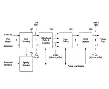
present invention.
[24] FIG. 15 illustrates PLS2 data according to another embodiment of the
present invention.
[25] FIG. 16 illustrates a logical structure of a frame according to an
embodiment of the present
invention.
[26] FIG. 17 illustrates PLS mapping according to an embodiment of the
present invention.
[27] FIG. 18 illustrates EAC mapping according to an embodiment of the
present invention.
[28] FIG. 19 illustrates FIC mapping according to an embodiment of the
present invention.
[29] FIG. 20 illustrates a type of DP according to an embodiment of the
present invention.
[30] FIG. 21 illustrates DP mapping according to an embodiment of the
present invention.
[31] FIG. 22 illustrates an FEC structure according to an embodiment of the
present invention.
[32] FIG. 23 illustrates a bit interleaving according to an embodiment of
the present invention.
[33] FIG. 24 illustrates a cell-word demultiplexing according to an
embodiment of the present
invention.
[34] FIG. 25 illustrates a time interleaving according to an embodiment of
the present invention.
[35] FIG. 26 illustrates the basic operation of a twisted row-column block
interleaver according
to an embodiment of the present invention.
[36] FIG. 27 illustrates an operation of a twisted row-column block
interleaver according to
another embodiment of the present invention.
[37] FIG. 28 illustrates a diagonal-wise reading pattern of a twisted row-
column block interleaver
according to an embodiment of the present invention.
[38] FIG. 29 illustrates interlaved XFECBLOCKs from each interleaving array
according to an
embodiment of the present invention.
3
CA 02943822 2016-09-23
[39] FIG. 30 illustrates a time interleaving process according to an
embodiment of the present
invention.
[40] FIG. 31 illustrates a time interleaving process according to another
embodiment of the
present invention.
[41] FIG. 32 illustrates a process of generating TI output memory indexes
according to an
embodiment of the present invention.
[42] FIG. 33 illustrates a time deinterleaving process according to an
embodiment of the present
invention.
[43] FIG. 34 illustrates a time deinterleaving process according to another
embodiment of the
present invention.
[44] FIG. 35 illustrates a process of generating TDI output memory indexes
according to an
embodiment of the present invention.
[45] FIG. 36 is a conceptual diagram illustrating a variable data-rate
system according to an
embodiment of the present invention.
[46] FIG. 37 illustrates a time interleaving process according to another
embodiment of the
present invention.
[47] FIG. 38 illustrates a process of generating TI output memory indexes
according to another
embodiment of the present invention.
[48] FIG. 39 is a flowchart illustrating a TI memory index generation
process according to an
embodiment of the present invention.
[49] FIG. 40 illustrates a time deinterleaving process according to another
embodiment of the
present invention.
[50] FIG. 41 illustrates a time deinterleaving process according to another
embodiment of the
present invention.
[51] FIG. 42 illustrates a writing method according to an embodiment of the
present invention.
[52] FIG. 43 is a flowchart illustrating a process of generating TDI memory
indexes according to
an embodiment of the present invention.
[53] FIG. 44 illustrates a time interleaving process according to another
embodiment of the
present invention.
[54] FIG. 45 illustrates diagonal slopes according to an embodiment of the
present invention.
[55] FIG. 46 illustrates a time deinterleaving process according to an
embodiment of the present
invention.
4
CA 02943822 2016-09-23
[56] FIG. 47 illustrates a process of generating TDI output memory indexes
according to an
embodiment of the present invention.
[57] FIG. 48 is a conceptual diagram illustrating a variable data-rate
system according to an
embodiment of the present invention.
[58] FIG. 49 is a flowchart illustrating a process of generating TDI memory
indexes according to
an embodiment of the present invention.
[59] FIG. 50 illustrates IF-by-IF TI pattern variation according to an
embodiment of the present
invention.
[60] FIG 51 illustrates IF interleaving according to an embodiment of the
present invention.
[61] FIG. 52 illustrates CI according to an embodiment of the present
invention.
[62] FIG. 53 illustrates Cl according to another embodiment of the present
invention.
[63] FIG. 54 illustrates output IFs of Cl according to an embodiment of the
present invention.
[64] FIG. 55 illustrates a time interleaver according to another embodiment
of the present
invention.
[65] FIG. 56 illustrates operation of the block interleaver according to an
embodiment of the
present invention.
[66] FIG. 57 illustrates operation of the block interleaver according to
another embodiment of the
present invention.
[67] FIG. 58 illustrates a time deinterleaver according to another
embodiment of the present
invention.
[68] FIG. 59 illustrates CI according to another embodiment of the present
invention.
[69] FIG. 60 illustrates interface processing between the convolutional
interleaver and the block
interleaver according to an embodiment of the present invention.
[70] FIG. 61 illustrates block interleaving according to another embodiment
of the present
invention.
[71] FIG. 62 illustrates the concept of a variable bit-rate system
according to an embodiment of
the present invention.
[72] FIG 63 illustrates writing and reading operations of block
interleaving according to an
embodiment of the present invention.
[73] FIG. 64 shows equations representing block interleaving according to
an embodiment of the
present invention.
[74] FIG. 65 illustrates virtual FEC blocks according to an embodiment of
the present invention.
CA 02943822 2016-09-23
[75] FIG. 66 shows equations representing reading operation after insertion
of virtual FEC blocks
according to an embodiment of the present invention.
[76] FIG. 67 is a flowchart illustrating a time interleaving process
according to an embodiment of
the present invention.
[77] FIG. 68 shows equations representing a process of determining a shift
value and a maximum
TI block size according to an embodiment of the present invention.
[78] FIG. 69 illustrates writing operation according to an embodiment of
the present invention.
[79] FIG. 70 illustrates reading operation according to an embodiment of
the present invention.
[80] FIG. 71 illustrates a result of skip operation in reading operation
according to an
embodiment of the present invention.
[81] FIG. 72 shows a writing process of time deinterleaving according to an
embodiment of the
present invention.
[82] FIG. 73 illustrates a writing process of time deinterleaving according
to another embodiment
of the present invention.
[83] FIG. 74 shows equations representing reading operation of time
deinterleaving according to
another embodiment of the present invention.
[84] FIG. 75 is a flowchart illustrating a time deinterleaving process
according to an embodiment
of the present invention.
[85] FIG. 76 is a flowchart illustrating a method for transmitting
broadcast signals accordi
ng to an embodiment of the present invention.
[Best Mode]
[86] Reference will now be made in detail to the preferred embodiments of
the present invention,
examples of which are illustrated in the accompanying drawings. The detailed
description, which will
be given below with reference to the accompanying drawings, is intended to
explain exemplary
embodiments of the present invention, rather than to show the only embodiments
that can be implemented
according to the present invention. The following detailed description
includes specific details in order
to provide a thorough understanding of the present invention. However, it will
be apparent to those
skilled in the art that the present invention may be practiced without such
specific details.
[87] Although most terms used in the present invention have been selected
from general ones
widely used in the art, some terms have been arbitrarily selected by the
applicant and their meanings are
6
CA 02943822 2016-09-23
explained in detail in the following description as needed. Thus, the present
invention should be
understood based upon the intended meanings of the terms rather than their
simple names or meanings.
[88] The present invention provides apparatuses and methods for
transmitting and receiving
broadcast signals for future broadcast services. Future broadcast services
according to an embodiment
of the present invention include a terrestrial broadcast service, a mobile
broadcast service, a UHDTV
service, etc. The present invention may process broadcast signals for the
future broadcast services
through non-MIMO (Multiple Input Multiple Output) or MIMO according to one
embodiment. A non-
MIMO scheme according to an embodiment of the present invention may include a
MISO (Multiple Input
Single Output) scheme, a SISO (Single Input Single Output) scheme, etc.
[89] While MISO or MIMO uses two antennas in the following for convenience
of description,
the present invention is applicable to systems using two or more antennas.
[90] The present invention may defines three physical layer (PL) profiles ¨
base, handheld and
advanced profiles¨each optimized to minimize receiver complexity while
attaining the performance
required for a particular use case. The physical layer (PHY) profiles are
subsets of all configurations that
a corresponding receiver should implement.
[91] The three PHY profiles share most of the functional blocks but differ
slightly in specific
blocks and/or parameters. Additional PHY profiles can be defined in the
future. For the system evolution,
future profiles can also be multiplexed with the existing profiles in a single
RF channel through a future
extension frame (FEF). The details of each PHY profile are described below.
[92] 1. Base profile
[93] The base profile represents a main use case for fixed receiving
devices that are usually
connected to a roof-top antenna. The base profile also includes portable
devices that could be transported
to a place but belong to a relatively stationary reception category. Use of
the base profile could be
extended to handheld devices or even vehicular by some improved
implementations, but those use cases
are not expected for the base profile receiver operation.
[94] Target SNR range of reception is from approximately 10 to 20dB, which
includes the 15dB
SNR reception capability of the existing broadcast system (e.g. ATSC A/53).
The receiver complexity
and power consumption is not as critical as in the battery-operated handheld
devices, which will use the
handheld profile. Key system parameters for the base profile are listed in
below table 1.
[95] [Table 1]
LDPC codeword length 16K, 64K bits
7
CA 02943822 2016-09-23
Constellation size 4-10 bpcu (bits per channel use)
Time de-interleaving memory size < 219 data cells
Pilot patterns Pilot pattern for fixed reception
FFT size 16K, 32K points
[96] 2. Handheld profile
[97] The handheld profile is designed for use in handheld and vehicular
devices that operate with
battery power. The devices can be moving with pedestrian or vehicle speed. The
power consumption as
well as the receiver complexity is very important for the implementation of
the devices of the handheld
profile. The target SNR range of the handheld profile is approximately 0 to
10dB, but can be configured
to reach below OdB when intended for deeper indoor reception.
[98] In addition to low SNR capability, resilience to the Doppler Effect
caused by receiver
mobility is the most important performance attribute of the handheld profile.
Key system parameters for
the handheld profile are listed in the below table 2.
[99] [Table 2]
LDPC codeword length 16K bits
Constellation size 2-8 bpcu
Time de-interleaving memory size < 218 data cells
Pilot patterns Pilot patterns for mobile and indoor
reception
FFT size 8K, 16K points
1100] 3. Advanced profile
[101] The advanced profile provides highest channel capacity at the cost of
more implementation
complexity. This profile requires using MIMO transmission and reception, and
UHDTV service is a target
use case for which this profile is specifically designed. The increased
capacity can also be used to allow
an increased number of services in a given bandwidth, e.g., multiple SDTV or
HDTV services.
[102] The target SNR range of the advanced profile is approximately 20 to
30dB. MIMO
transmission may initially use existing elliptically-polarized transmission
equipment, with extension to
full-power cross-polarized transmission in the future. Key system parameters
for the advanced profile are
listed in below table 3.
[103] [Table 3]
LDPC codeword length 16K, 64K bits
Constellation size 8-12 bpcu
8
CA 02943822 2016-09-23
Time de-interleaving memory size < 219 data cells
Pilot patterns Pilot pattern for fixed reception
FFT size 16K, 32K points
[104] In this case, the base profile can be used as a profile for both the
terrestrial broadcast service
and the mobile broadcast service. That is, the base profile can be used to
define a concept of a profile
which includes the mobile profile. Also, the advanced profile can be divided
advanced profile for a base
profile with MIMO and advanced profile for a handheld profile with MIMO.
Moreover, the three profiles
can be changed according to intention of the designer.
[105] The following terms and definitions may apply to the present
invention. The following
terms and definitions can be changed according to design.
1106] auxiliary stream: sequence of cells carrying data of as yet undefined
modulation and coding,
which may be used for future extensions or as required by broadcasters or
network operators
[107] base data pipe: data pipe that carries service signaling data
[108] baseband frame (or BBFRAME): set of Kbch bits which form the input to
one FEC
encoding process (BCH and LDPC encoding)
[109] cell: modulation value that is carried by one carrier of the OFDM
transmission
[110] coded block: LDPC-encoded block of PLS1 data or one of the LDPC-
encoded blocks of
PLS2 data
[111] data pipe: logical channel in the physical layer that carries service
data or related metadata,
which may carry one or multiple service(s) or service component(s).
[112] data pipe unit: a basic unit for allocating data cells to a DP in a
frame.
[113] data symbol: OFDM symbol in a frame which is not a preamble symbol
(the frame signaling
symbol and frame edge symbol is included in the data symbol)
[114] DP_ID: this 8-bit field identifies uniquely a DP within the system
identified by the
SYSTEM_ID
[115] dummy cell: cell carrying a pseudo-random value used to fill the
remaining capacity not
used for PLS signaling, DPs or auxiliary streams
[116] emergency alert channel: part of a frame that carries EAS information
data
[117] frame: physical layer time slot that starts with a preamble and ends
with a frame edge
symbol
[118] frame repetition unit: a set of frames belonging to same or different
physical layer profile
including a FEF, which is repeated eight times in a super-frame
9
CA 02943822 2016-09-23
[119] fast information channel: a logical channel in a frame that carries
the mapping information
between a service and the corresponding base DP
[120] FECBLOCK: set of LDPC-encoded bits of a DP data
[121] FFT size: nominal FFT size used for a particular mode, equal to the
active symbol period Ts
expressed in cycles of the elementary period T
[122] frame signaling symbol: OFDM symbol with higher pilot density used at
the start of a frame
in certain combinations of FFT size, guard interval and scattered pilot
pattern, which carries a part of the
PLS data
[123] frame edge symbol: OFDM symbol with higher pilot density used at the
end of a frame in
certain combinations of FFT size, guard interval and scattered pilot pattern
[124] frame-group: the set of all the frames having the same PRY profile
type in a super-frame.
[125] future extension frame: physical layer time slot within the super-
frame that could be used
for future extension, which starts with a preamble
[126] Futurecast UTB system: proposed physical layer broadcasting system,
of which the input is
one or more MPEG2-TS or IP or general stream(s) and of which the output is an
RF signal
[127] input stream: A stream of data for an ensemble of services delivered
to the end users by the
system.
[128] normal data symbol: data symbol excluding the frame signaling symbol
and the frame edge
symbol
[129] PHY profile: subset of all configurations that a corresponding
receiver should implement
[130] PLS: physical layer signaling data consisting of PLS1 and PLS2
[131] PLS1: a first set of PLS data carried in the FSS symbols having a
fixed size, coding and
modulation, which carries basic information about the system as well as the
parameters needed to decode
the PLS2
[132] NOTE: PLS1 data remains constant for the duration of a frame-
group.
[133] PLS2: a second set of PLS data transmitted in the FSS symbol, which
carries more detailed
PLS data about the system and the DPs
[134] PLS2 dynamic data: PLS2 data that may dynamically change frame-by-
frame
[135] PLS2 static data: PLS2 data that remains static for the duration of a
frame-group
[136] preamble signaling data: signaling data carried by the preamble
symbol and used to identify
the basic mode of the system
[137] preamble symbol: fixed-length pilot symbol that carries basic PLS
data and is located in the
CA 02943822 2016-09-23
beginning of a frame
[138] NOTE: The preamble symbol is mainly used for fast initial band
scan to detect the
system signal, its timing, frequency offset, and FFT-size.
[139] reserved for future use: not defined by the present document but may
be defined in future
[140] super-frame: set of eight frame repetition units
[141] time interleaving block (TI block): set of cells within which time
interleaving is carried out,
corresponding to one use of the time interleaver memory
[142] TI group: unit over which dynamic capacity allocation for a
particular DP is carried out,
made up of an integer, dynamically varying number of XFECBLOCKs
[143] NOTE: The TI group may be mapped directly to one frame or may be
mapped to
multiple frames. It may contain one or more T1 blocks.
[144] Type 1 DP: DP of a frame where all DPs are mapped into the frame in
TDM fashion
[145] Type 2 DP: DP of a frame where all DPs are mapped into the frame in
FDM fashion
[146] XFECBLOCK: set of Ncells cells carrying all the bits of one LDPC
FECBLOCK
[147] FIG. 1 illustrates a structure of an apparatus for transmitting
broadcast signals for future
broadcast services according to an embodiment of the present invention.
[148] The apparatus for transmitting broadcast signals for future broadcast
services according to
an embodiment of the present invention can include an input formatting block
1000, a BICM (Bit
interleaved coding & modulation) block 1010, a frame building block 1020, an
OFDM (Orthogonal
Frequency Division Multiplexing) generation block 1030 and a signaling
generation block 1040. A
description will be given of the operation of each module of the apparatus for
transmitting broadcast
signals.
[149] IP stream/packets and MPEG2-TS are the main input formats, other
stream types are
handled as General Streams. In addition to these data inputs, Management
Information is input to control
the scheduling and allocation of the corresponding bandwidth for each input
stream. One or multiple TS
stream(s), IP stream(s) and/or General Stream(s) inputs are simultaneously
allowed.
[150] The input formatting block 1000 can demultiplex each input stream
into one or multiple data
pipe(s), to each of which an independent coding and modulation is applied. The
data pipe (DP) is the
basic unit for robustness control, thereby affecting quality-of-service (QoS).
One or multiple service(s) or
service component(s) can be carried by a single DP. Details of operations of
the input formatting block
1000 will be described later.
[151] The data pipe is a logical channel in the physical layer that carries
service data or related
11
CA 02943822 2016-09-23
metadata, which may carry one or multiple service(s) or service component(s).
[152] Also, the data pipe unit: a basic unit for allocating data cells to a
DP in a frame.
[153] In the BICM block 1010, parity data is added for error correction and
the encoded bit
streams are mapped to complex-value constellation symbols. The symbols are
interleaved across a
specific interleaving depth that is used for the corresponding DP. For the
advanced profile, MIMO
encoding is performed in the BICM block 1010 and the additional data path is
added at the output for
MIMO transmission. Details of operations of the BICM block 1010 will be
described later.
[154] The Frame Building block 1020 can map the data cells of the input DPs
into the OFDM
symbols within a frame. After mapping, the frequency interleaving is used for
frequency-domain diversity,
especially to combat frequency-selective fading channels. Details of
operations of the Frame Building
block 1020 will be described later.
[155] After inserting a preamble at the beginning of each frame, the OFDM
Generation block
1030 can apply conventional OFDM modulation having a cyclic prefix as guard
interval. For antenna
space diversity, a distributed MISO scheme is applied across the transmitters.
In addition, a Peak-to-
Average Power Reduction (PAPR) scheme is performed in the time domain. For
flexible network
planning, this proposal provides a set of various FFT sizes, guard interval
lengths and corresponding pilot
patterns. Details of operations of the OFDM Generation block 1030 will be
described later.
[156] The Signaling Generation block 1040 can create physical layer
signaling information used
for the operation of each functional block. This signaling information is also
transmitted so that the
services of interest are properly recovered at the receiver side. Details of
operations of the Signaling
Generation block 1040 will be described later.
[157] FIGS. 2, 3 and 4 illustrate the input formatting block 1000 according
to embodiments of the
present invention. A description will be given of each figure.
[158] FIG. 2 illustrates an input formatting block according to one
embodiment of the present
invention. FIG. 2 shows an input formatting module when the input signal is a
single input stream.
[159] The input formatting block illustrated in FIG. 2 corresponds to an
embodiment of the input
formatting block 1000 described with reference to FIG. 1.
[160[ The input to the physical layer may be composed of one or multiple
data streams. Each data
stream is carried by one DP. The mode adaptation modules slice the incoming
data stream into data fields
of the baseband frame (BBF). The system supports three types of input data
streams: MPEG2-TS, Internet
protocol (IP) and Generic stream (GS). MPEG2-TS is characterized by fixed
length (188 byte) packets
with the first byte being a sync-byte (0x47). An IP stream is composed of
variable length IP datagram
packets, as signaled within IP packet headers. The system supports both IPv4
and IPv6 for the IP stream.
12
CA 02943822 2016-09-23
GS may be composed of variable length packets or constant length packets,
signaled within encapsulation
packet headers.
[161] (a) shows a mode adaptation block 2000 and a stream adaptation 2010
for signal DP and (b)
shows a PLS generation block 2020 and a PLS scrambler 2030 for generating and
processing PLS data. A
description will be given of the operation of each block.
[162] The Input Stream Splitter splits the input TS, IP, GS streams into
multiple service or service
component (audio, video, etc.) streams. The mode adaptation module 2010 is
comprised of a CRC
Encoder, BB (baseband) Frame Slicer, and BB Frame Header Insertion block.
[163] The CRC Encoder provides three kinds of CRC encoding for error
detection at the user
packet (UP) level, i.e., CRC-8, CRC-16, and CRC-32. The computed CRC bytes are
appended after the
UP. CRC-8 is used for IS stream and CRC-32 for IP stream. If the GS stream
doesn't provide the CRC
encoding, the proposed CRC encoding should be applied.
[164] BB Frame Slicer maps the input into an internal logical-bit format.
The first received bit is
defined to be the MSB. The BB Frame Slicer allocates a number of input bits
equal to the available data
field capacity. To allocate a number of input bits equal to the BBF payload,
the UP packet stream is sliced
to fit the data field of BBF.
[165] BB Frame Header Insertion block can insert fixed length BBF header of
2 bytes is inserted
in front of the BB Frame. The BBF header is composed of STUFFI (1 bit), SYNCD
(13 bits), and RFU (2
bits). In addition to the fixed 2-Byte BBF header, BBF can have an extension
field (1 or 3 bytes) at the
end of the 2-byte BBF header.
[166] The stream adaptation 2010 is comprised of stuffing insertion block
and BB scrambler.
[167] The stuffing insertion block can insert stuffing field into a payload
of a BB frame. If the
input data to the stream adaptation is sufficient to fill a BB-Frame, STUFFI
is set to '0' and the BBF has
no stuffing field. Otherwise STUFFI is set to '1' and the stuffing field is
inserted immediately after the
BBF header. The stuffing field comprises two bytes of the stuffing field
header and a variable size of
stuffing data.
[168] The BB scrambler scrambles complete BBF for energy dispersal. The
scrambling sequence
is synchronous with the BBF. The scrambling sequence is generated by the feed-
back shift register.
[169] The PLS generation block 2020 can generate physical layer signaling
(PLS) data. The PLS
provides the receiver with a means to access physical layer DPs. The PLS data
consists of PLS1 data and
PLS2 data.
[170] The PLS1 data is a first set of PLS data carried in the FSS symbols
in the frame having a
fixed size, coding and modulation, which carries basic information about the
system as well as the
13
CA 02943822 2016-09-23
parameters needed to decode the PLS2 data. The PLS1 data provides basic
transmission parameters
including parameters required to enable the reception and decoding of the PLS2
data. Also, the PLS1 data
remains constant for the duration of a frame-group.
[171] The PLS2 data is a second set of PLS data transmitted in the FSS
symbol, which carries
more detailed PLS data about the system and the DPs. The PLS2 contains
parameters that provide
sufficient information for the receiver to decode the desired DP. The PLS2
signaling further consists of
two types of parameters, PLS2 Static data (PLS2-STAT data) and PLS2 dynamic
data (PLS2-DYN data).
The PLS2 Static data is PLS2 data that remains static for the duration of a
frame-group and the PLS2
dynamic data is PLS2 data that may dynamically change frame-by-frame.
[172] Details of the PLS data will be described later.
[173] The PLS scrambler 2030 can scramble the generated PLS data for energy
dispersal.
[174] The above-described blocks may be omitted or replaced by blocks
having similar or
identical functions.
[175] FIG. 3 illustrates an input formatting block according to another
embodiment of the present
invention.
[176] The input formatting block illustrated in FIG. 3 corresponds to an
embodiment of the input
formatting block 1000 described with reference to FIG. 1.
[177] FIG. 3 shows a mode adaptation block of the input formatting block
when the input signal
corresponds to multiple input streams.
[178] The mode adaptation block of the input formatting block for
processing the multiple input
streams can independently process the multiple input streams.
[179] Referring to FIG. 3, the mode adaptation block for respectively
processing the multiple
input streams can include an input stream splitter 3000, an input stream
synchronizer 3010, a
compensating delay block 3020, a null packet deletion block 3030, a head
compression block 3040, a
CRC encoder 3050, a BB frame slicer 3060 and a BB header insertion block 3070.
Description will be
given of each block of the mode adaptation block.
[180] Operations of the CRC encoder 3050, BB frame slicer 3060 and BB
header insertion block
3070 correspond to those of the CRC encoder, BB frame slicer and BB header
insertion block described
with reference to FIG. 2 and thus description thereof is omitted.
[181] The input stream splitter 3000 can split the input TS, IP, GS streams
into multiple service or
service component (audio, video, etc.) streams.
[182] The input stream synchronizer 3010 may be referred as ISSY. The ISSY
can provide
suitable means to guarantee Constant Bit Rate (CBR) and constant end-to-end
transmission delay for any
14
CA 02943822 2016-09-23
input data format. The ISSY is always used for the case of multiple DPs
carrying IS, and optionally used
for multiple DPs carrying GS streams.
[183] The compensating delay block 3020 can delay the split TS packet
stream following the
insertion of ISSY information to allow a TS packet recombining mechanism
without requiring additional
memory in the receiver.
[184] The null packet deletion block 3030, is used only for the TS input
stream case. Some TS
input streams or split TS streams may have a large number of null-packets
present in order to
accommodate VBR (variable bit-rate) services in a CBR TS stream. In this case,
in order to avoid
unnecessary transmission overhead, null-packets can be identified and not
transmitted. In the receiver,
removed null-packets can be re-inserted in the exact place where they were
originally by reference to a
deleted null-packet (DNP) counter that is inserted in the transmission, thus
guaranteeing constant bit-rate
and avoiding the need for time-stamp (PCR) updating.
[185] The head compression block 3040 can provide packet header compression
to increase
transmission efficiency for TS or IP input streams. Because the receiver can
have a priori information on
certain parts of the header, this known information can be deleted in the
transmitter.
[186] For Transport Stream, the receiver has a-priori information about the
sync-byte
configuration (0x47) and the packet length (188 Byte). If the input TS stream
carries content that has only
one PID, i.e., for only one service component (video, audio, etc.) or service
sub-component (SVC base
layer, SVC enhancement layer, MVC base view or MVC dependent views), TS packet
header
compression can be applied (optionally) to the Transport Stream. IP packet
header compression is used
optionally if the input steam is an IP stream.
[187] The above-described blocks may be omitted or replaced by blocks
having similar or
identical functions.
[188] FIG. 4 illustrates an input formatting block according to another
embodiment of the present
invention.
[189] The input formatting block illustrated in FIG. 4 corresponds to an
embodiment of the input
formatting block 1000 described with reference to FIG. 1.
[190] FIG. 4 illustrates a stream adaptation block of the input formatting
module when the input
signal corresponds to multiple input streams.
[191] Referring to FIG. 4, the mode adaptation block for respectively
processing the multiple
input streams can include a scheduler 4000, an 1-Frame delay block 4010, a
stuffing insertion block 4020,
an in-band signaling 4030, a BB Frame scrambler 4040, a PLS generation block
4050 and a PLS
scrambler 4060. Description will be given of each block of the stream
adaptation block.
CA 02943822 2016-09-23
[192] Operations of the stuffing insertion block 4020, the BB Frame
scrambler 4040, the PLS
generation block 4050 and the PLS scrambler 4060 correspond to those of the
stuffing insertion block,
BB scrambler, PLS generation block and the PLS scrambler described with
reference to FIG. 2 and thus
description thereof is omitted.
[193] The scheduler 4000 can determine the overall cell allocation across
the entire frame from
the amount of FECBLOCKs of each DP. Including the allocation for PLS, EAC and
FIC, the scheduler
generate the values of PLS2-DYN data, which is transmitted as in-band
signaling or PLS cell in FSS of
the frame. Details of FECBLOCK, EAC and FIC will be described later.
[194] The 1-Frame delay block 4010 can delay the input data by one
transmission frame such that
scheduling information about the next frame can be transmitted through the
current frame for in-band
signaling information to be inserted into the DPs.
[195] The in-band signaling 4030 can insert un-delayed part of the PLS2
data into a DP of a frame.
[196] The above-described blocks may be omitted or replaced by blocks
having similar or
identical functions.
[197] FIG. 5 illustrates a BICM block according to an embodiment of the
present invention.
[198] The BICM block illustrated in FIG. 5 corresponds to an embodiment of
the BICM block
1010 described with reference to FIG. I.
[199] As described above, the apparatus for transmitting broadcast signals
for future broadcast
services according to an embodiment of the present invention can provide a
terrestrial broadcast service,
mobile broadcast service, UHDTV service, etc.
[200] Since QoS (quality of service) depends on characteristics of a
service provided by the
apparatus for transmitting broadcast signals for future broadcast services
according to an embodiment of
the present invention, data corresponding to respective services needs to be
processed through different
schemes. Accordingly, the a BICM block according to an embodiment of the
present invention can
independently process DPs input thereto by independently applying SISO, MISO
and MIMO schemes to
the data pipes respectively corresponding to data paths. Consequently, the
apparatus for transmitting
broadcast signals for future broadcast services according to an embodiment of
the present invention can
control QoS for each service or service component transmitted through each DP.
[201] (a) shows the BICM block shared by the base profile and the handheld
profile and (b) shows
the BICM block of the advanced profile.
[202] The BICM block shared by the base profile and the handheld profile
and the BICM block of
the advanced profile can include plural processing blocks for processing each
DP.
[203] A description will be given of each processing block of the BICM
block for the base profile
16
CA 02943822 2016-09-23
and the handheld profile and the BICM block for the advanced profile.
[204] A processing block 5000 of the BICM block for the base profile and
the handheld profile
can include a Data FEC encoder 5010, a bit interleaver 5020, a constellation
mapper 5030, an SSD
(Signal Space Diversity) encoding block 5040 and a time interleaver 5050.
[205] The Data FEC encoder 5010 can perform the FEC encoding on the input
BBF to generate
FECBLOCK procedure using outer coding (BCH), and inner coding (LDPC). The
outer coding (BCH) is
optional coding method. Details of operations of the Data FEC encoder 5010
will be described later.
[206] The bit interleaver 5020 can interleave outputs of the Data FEC
encoder 5010 to achieve
optimized performance with combination of the LDPC codes and modulation scheme
while providing an
efficiently implementable structure. Details of operations of the bit
interleaver 5020 will be described
later.
[207] The constellation mapper 5030 can modulate each cell word from the
bit interleaver 5020 in
the base and the handheld profiles, or cell word from the Cell-word
demultiplexer 5010-1 in the advanced
profile using either QPSK, QAM-16, non-uniform QAM (NUQ-64, NUQ-256, NUQ-1024)
or non-
uniform constellation (NUC-16, NUC-64, NUC-256, NUC-1024) to give a power-
normalized
constellation point, el. This constellation mapping is applied only for DPs.
Observe that QAM-16 and
NUQs are square shaped, while NUCs have arbitrary shape. When each
constellation is rotated by any
multiple of 90 degrees, the rotated constellation exactly overlaps with its
original one. This "rotation-
sense" symmetric property makes the capacities and the average powers of the
real and imaginary
components equal to each other. Both NUQs and NUCs are defined specifically
for each code rate and the
particular one used is signaled by the parameter DP MOD filed in PLS2 data.
[208] The SSD encoding block 5040 can precode cells in two (2D), three
(3D), and four (4D)
dimensions to increase the reception robustness under difficult fading
conditions.
[209] The time interleaver 5050 can operates at the DP level. The
parameters of time interleaving
(TI) may be set differently for each DP. Details of operations of the time
interleaver 5050 will be
described later.
[210] A processing block 5000-1 of the BICM block for the advanced profile
can include the Data
FEC encoder, bit interleaver, constellation mapper, and time interleaver.
However, the processing block
5000-1 is distinguished from the processing block 5000 further includes a cell-
word demultiplexer 5010-1
and a MIMO encoding block 5020-1.
[211] Also, the operations of the Data FEC encoder, bit interleaver,
constellation mapper, and time
interleaver in the processing block 5000-1 correspond to those of the Data FEC
encoder 5010, bit
interleaver 5020, constellation mapper 5030, and time interleaver 5050
described and thus description
17
CA 02943822 2016-09-23
thereof is omitted.
[212] The cell-word demultiplexer 5010-1 is used for the DP of the advanced
profile to divide the
single cell-word stream into dual cell-word streams for MIMO processing.
Details of operations of the
cell-word demultiplexer 5010-1 will be described later.
[213] The MIMO encoding block 5020-1 can processing the output of the cell-
word demultiplexer
5010-1 using MIMO encoding scheme. The MIMO encoding scheme was optimized for
broadcasting
signal transmission. The MIMO technology is a promising way to get a capacity
increase but it depends
on channel characteristics. Especially for broadcasting, the strong LOS
component of the channel or a
difference in the received signal power between two antennas caused by
different signal propagation
characteristics makes it difficult to get capacity gain from MIMO. The
proposed MIMO encoding scheme
overcomes this problem using a rotation-based pre-coding and phase
randomization of one of the MIMO
output signals.
[214] MIMO encoding is intended for a 2x2 MIMO system requiring at least
two antennas at both
the transmitter and the receiver. Two MIMO encoding modes are defined in this
proposal; full-rate spatial
multiplexing (FR-SM) and full-rate full-diversity spatial multiplexing (FRFD-
SM). The FR-SM encoding
provides capacity increase with relatively small complexity increase at the
receiver side while the FRFD-
SM encoding provides capacity increase and additional diversity gain with a
great complexity increase at
the receiver side. The proposed MIMO encoding scheme has no restriction on the
antenna polarity
configuration.
[215] MIMO processing is required for the advanced profile frame, which
means all DPs in the
advanced profile frame are processed by the MIMO encoder. MIMO processing is
applied at DP level.
Pairs of the Constellation Mapper outputs NUQ (el,i and e2,i) are fed to the
input of the MIMO Encoder.
Paired MIMO Encoder output (g 1,i and 82,i) is transmitted by the same carrier
k and OFDM symbol 1 of
their respective TX antennas.
[216] The above-described blocks may be omitted or replaced by blocks
having similar or
identical functions.
[217] FIG. 6 illustrates a BICM block according to another embodiment of
the present invention.
[218] The BICM block illustrated in FIG. 6 corresponds to an embodiment of
the BICM block
1010 described with reference to FIG. 1.
[219] FIG. 6 illustrates a BICM block for protection of physical layer
signaling (PLS), emergency
alert channel (EAC) and fast information channel (FTC). EAC is a part of a
frame that carries EAS
information data and FIC is a logical channel in a frame that carries the
mapping information between a
service and the corresponding base DP. Details of the EAC and FTC will be
described later.
18
CA 02943822 2016-09-23
=
[220] Referring to FIG. 6, the BICM block for protection of PLS, EAC and
FIC can include a PLS
FEC encoder 6000, a bit interleaver 6010 and a constellation mapper 6020.
[221] Also, the PLS FEC encoder 6000 can include a scrambler, BCH
encoding/zero insertion
block, LDPC encoding block and LDPC parity punturing block. Description will
be given of each block
of the BICM block.
[222] The PLS FEC encoder 6000 can encode the scrambled PLS 1/2 data, EAC
and FIC section.
[223] The scrambler can scramble PLS1 data and PLS2 data before BCH
encoding and shortened
and punctured LDPC encoding.
1224] The BCH encoding/zero insertion block can perform outer encoding
on the scrambled PLS
1/2 data using the shortened BCH code for PLS protection and insert zero bits
after the BCH encoding.
For PLS1 data only, the output bits of the zero insertion may be permutted
before LDPC encoding.
[225] The LDPC encoding block can encode the output of the BCH
encoding/zero insertion block
using LDPC code. To generate a complete coded block, Cldpc, parity bits, Pldpc
are encoded
systematically from each zero-inserted PLS information block, Ildpc and
appended after it.
[226] [Math figure 1]
[227] Chip,= [ I icipc Ph/pc.] = [ '" = PO, Pi
[228] The LDPC code parameters for PLS1 and PLS2 are as following table
4.
[229] [Table 4]
Signaling Kldpc code
Ksig Kbch Nbch_panty Nidpc NIdpc_parity Qldpc
Type (=Nbch) rate
PLS1 342
1020 1080 4320 3240 1/4 36
<1021 60
PLS2
>1020 2100 2160 7200 5040 3/10 56
[230] The LDPC parity punturing block can perform puncturing on the
PLS1 data and PLS 2 data.
[231] When shortening is applied to the PLS1 data protection, some LDPC
parity bits are
punctured after LDPC encoding. Also, for the PLS2 data protection, the LDPC
parity bits of PLS2 are
punctured after LDPC encoding. These punctured bits are not transmitted.
[232] The bit interleaver 6010 can interleave the each shortened and
punctured PLS1 data and
PLS2 data.
[233] The constellation mapper 6020 can map the bit ineterlaeved PLS1
data and PLS2 data onto
constellations.
19
CA 02943822 2016-09-23
[234] The above-described blocks may be omitted or replaced by blocks
having similar or
identical functions.
[235] FIG. 7 illustrates a frame building block according to one embodiment
of the present
invention.
[236] The frame building block illustrated in FIG. 7 corresponds to an
embodiment of the frame
building block 1020 described with reference to FIG. 1.
[237] Referring to FIG. 7, the frame building block can include a delay
compensation block 7000,
a cell mapper 7010 and a frequency interleaver 7020. Description will be given
of each block of the frame
building block.
[238] The delay compensation block 7000 can adjust the timing between the
data pipes and the
corresponding PLS data to ensure that they are co-timed at the transmitter
end. The PLS data is delayed
by the same amount as data pipes are by addressing the delays of data pipes
caused by the Input
Formatting block and BICM block. The delay of the BICM block is mainly due to
the time interleaver
5050. In-band signaling data carries information of the next TI group so that
they are carried one frame
ahead of the DPs to be signaled. The Delay Compensating block delays in-band
signaling data
accordingly.
[239] The cell mapper 7010 can map PLS, EAC, FTC, DPs, auxiliary streams
and dummy cells
into the active carriers of the OFDM symbols in the frame. The basic function
of the cell mapper 7010 is
to map data cells produced by the TTs for each of the DPs, PLS cells, and
EAC/FIC cells, if any, into
arrays of active OFDM cells corresponding to each of the OFDM symbols within a
frame. Service
signaling data (such as PSI(program specific information)/SI) can be
separately gathered and sent by a
data pipe. The Cell Mapper operates according to the dynamic information
produced by the scheduler and
the configuration of the frame structure. Details of the frame will be
described later.
[240] The frequency interleaver 7020 can randomly interleave data cells
received from the cell
mapper 7010 to provide frequency diversity. Also, the frequency interleaver
7020 can operate on very
OFDM symbol pair comprised of two sequential OFDM symbols using a different
interleaving-seed order
to get maximum interleaving gain in a single frame.
[241] The above-described blocks may be omitted or replaced by blocks
having similar or
identical functions.
[242] FIG. 8 illustrates an OFDM generation block according to an
embodiment of the present
invention.
[243] The OFDM generation block illustrated in FIG. 8 corresponds to an
embodiment of the
OFDM generation block 1030 described with reference to FIG. I.
CA 02943822 2016-09-23
[244] The OFDM generation block modulates the OFDM carriers by the cells
produced by the
Frame Building block, inserts the pilots, and produces the time domain signal
for transmission. Also, this
block subsequently inserts guard intervals, and applies PAPR (Peak-to-Average
Power Radio) reduction
processing to produce the final RF signal.
[245] Referring to FIG. 8, the OFDM generation block can include a pilot
and reserved tone
insertion block 8000, a 2D-eSFN encoding block 8010, an IFFT (Inverse Fast
Fourier Transform) block
8020, a PAPR reduction block 8030, a guard interval insertion block 8040, a
preamble insertion block
8050, other system insertion block 8060 and a DAC block 8070. Description will
be given of each block
of the frame building block.
[246] The pilot and reserved tone insertion block 8000 can insert pilots
and the reserved tone.
[247] Various cells within the OFDM symbol are modulated with reference
information, known as
pilots, which have transmitted values known a priori in the receiver. The
information of pilot cells is
made up of scattered pilots, continual pilots, edge pilots, FSS (frame
signaling symbol) pilots and FES
(frame edge symbol) pilots. Each pilot is transmitted at a particular boosted
power level according to pilot
type and pilot pattern. The value of the pilot information is derived from a
reference sequence, which is a
series of values, one for each transmitted carrier on any given symbol. The
pilots can be used for frame
synchronization, frequency synchronization, time synchronization, channel
estimation, and transmission
mode identification, and also can be used to follow the phase noise.
[248] Reference information, taken from the reference sequence, is
transmitted in scattered pilot
cells in every symbol except the preamble, FSS and FES of the frame. Continual
pilots are inserted in
every symbol of the frame. The number and location of continual pilots depends
on both the FFT size and
the scattered pilot pattern. The edge carriers are edge pilots in every symbol
except for the preamble
symbol. They are inserted in order to allow frequency interpolation up to the
edge of the spectrum. FSS
pilots are inserted in FSS(s) and FES pilots are inserted in FES. They are
inserted in order to allow time
interpolation up to the edge of the frame.
[249] The system according to an embodiment of the present invention
supports the SFN network,
where distributed MISO scheme is optionally used to support very robust
transmission mode. The 2D-
eSFN is a distributed MISO scheme that uses multiple TX antennas, each of
which is located in the
different transmitter site in the SFN network.
[250] The 2D-eSFN encoding block 8010 can process a 2D-eSFN processing to
distorts the phase
of the signals transmitted from multiple transmitters, in order to create both
time and frequency diversity
in the SFN configuration. Hence, burst errors due to low flat fading or deep-
fading for a long time can be
mitigated.
21
CA 02943822 2016-09-23
[251] The IFFT block 8020 can modulate the output from the 2D-eSFN encoding
block 8010
using OFDM modulation scheme. Any cell in the data symbols which has not been
designated as a pilot
(or as a reserved tone) carries one of the data cells from the frequency
interleaver. The cells are mapped to
OFDM carriers.
[252] The PAPR reduction block 8030 can perform a PAPR reduction on input
signal using
various PAPR reduction algorithm in the time domain.
[253] The guard interval insertion block 8040 can insert guard intervals
and the preamble insertion
block 8050 can insert preamble in front of the signal. Details of a structure
of the preamble will be
described later. The other system insertion block 8060 can multiplex signals
of a plurality of broadcast
transmission/reception systems in the time domain such that data of two or
more different broadcast
transmission/reception systems providing broadcast services can be
simultaneously transmitted in the
same RF signal bandwidth. In this case, the two or more different broadcast
transmission/reception
systems refer to systems providing different broadcast services. The different
broadcast services may refer
to a terrestrial broadcast service, mobile broadcast service, etc. Data
related to respective broadcast
services can be transmitted through different frames.
[254] The DAC block 8070 can convert an input digital signal into an analog
signal and output the
analog signal. The signal output from the DAC block 7800 can be transmitted
through multiple output
antennas according to the physical layer profiles. A Tx antenna according to
an embodiment of the
present invention can have vertical or horizontal polarity.
[255] The above-described blocks may be omitted or replaced by blocks
having similar or
identical functions according to design.
[256] FIG. 9 illustrates a structure of an apparatus for receiving
broadcast signals for future
broadcast services according to an embodiment of the present invention.
[257] The apparatus for receiving broadcast signals for future broadcast
services according to an
embodiment of the present invention can correspond to the apparatus for
transmitting broadcast signals
for future broadcast services, described with reference to FIG. 1.
[258] The apparatus for receiving broadcast signals for future broadcast
services according to an
embodiment of the present invention can include a synchronization &
demodulation module 9000, a
frame parsing module 9010, a demapping & decoding module 9020, an output
processor 9030 and a
signaling decoding module 9040. A description will be given of operation of
each module of the
apparatus for receiving broadcast signals.
[259] The synchronization & demodulation module 9000 can receive input
signals through m Rx
antennas, perform signal detection and synchronization with respect to a
system corresponding to the
22
CA 02943822 2016-09-23
apparatus for receiving broadcast signals and carry out demodulation
corresponding to a reverse
procedure of the procedure performed by the apparatus for transmitting
broadcast signals.
[260] The frame parsing module 9010 can parse input signal frames and
extract data through
which a service selected by a user is transmitted. If the apparatus for
transmitting broadcast signals
performs interleaving, the frame parsing module 9010 can carry out
deinterleaving corresponding to a
reverse procedure of interleaving. In this case, the positions of a signal and
data that need to be
extracted can be obtained by decoding data output from the signaling decoding
module 9040 to restore
scheduling information generated by the apparatus for transmitting broadcast
signals.
[261] The demapping & decoding module 9020 can convert the input signals
into bit domain data
and then deinterleave the same as necessary. The demapping & decoding module
9020 can perform
demapping for mapping applied for transmission efficiency and correct an error
generated on a
transmission channel through decoding. In this case, the demapping & decoding
module 9020 can
obtain transmission parameters necessary for demapping and decoding by
decoding the data output from
the signaling decoding module 9040.
[262] The output processor 9030 can perform reverse procedures of various
compression/signal
processing procedures which are applied by the apparatus for transmitting
broadcast signals to improve
transmission efficiency. In this case, the output processor 9030 can acquire
necessary control
information from data output from the signaling decoding module 9040. The
output of the output
processor 8300 corresponds to a signal input to the apparatus for transmitting
broadcast signals and may
be MPEG-TSs, IP streams (v4 or v6) and generic streams.
[263] The signaling decoding module 9040 can obtain PLS information from
the signal
demodulated by the synchronization & demodulation module 9000. As described
above, the frame
parsing module 9010, demapping & decoding module 9020 and output processor
9030 can execute
functions thereof using the data output from the signaling decoding module
9040.
[264] FIG. 10 illustrates a frame structure according to an embodiment of
the present invention.
[265] FIG. 10 shows an example configuration of the frame types and FRUs in
a super-frame. (a)
shows a super frame according to an embodiment of the present invention, (b)
shows FRU (Frame
Repetition Unit) according to an embodiment of the present invention, (c)
shows frames of variable PHY
profiles in the FRU and (d) shows a structure of a frame.
[266] A super-frame may be composed of eight FRUs. The FRU is a basic
multiplexing unit for
TDM of the frames, and is repeated eight times in a super-frame.
[267] Each frame in the FRU belongs to one of the PHY profiles, (base,
handheld, advanced) or
FEF. The maximum allowed number of the frames in the FRU is four and a given
PHY profile can appear
23
CA 02943822 2016-09-23
any number of times from zero times to four times in the FRU (e.g., base,
base, handheld, advanced).
PHY profile definitions can be extended using reserved values of the
PHY_PROFILE in the preamble, if
required.
[268] The FEF part is inserted at the end of the FRU, if included. When the
FEE is included in the
FRU, the minimum number of FEFs is 8 in a super-frame. It is not recommended
that FEF parts be
adjacent to each other.
[269] One frame is further divided into a number of OFDM symbols and a
preamble. As shown in
(d), the frame comprises a preamble, one or more frame signaling symbols
(FSS), normal data symbols
and a frame edge symbol (FES).
[270] The preamble is a special symbol that enables fast Futurecast UTB
system signal detection
and provides a set of basic transmission parameters for efficient transmission
and reception of the signal.
The detailed description of the preamble will be will be described later.
[271] The main purpose of the FSS(s) is to carry the PLS data. For fast
synchronization and
channel estimation, and hence fast decoding of PLS data, the FSS has more
dense pilot pattern than the
normal data symbol. The FES has exactly the same pilots as the FSS, which
enables frequency-only
interpolation within the FES and temporal interpolation, without
extrapolation, for symbols immediately
preceding the FES.
[272] FIG. 11 illustrates a signaling hierarchy structure of the frame
according to an embodiment
of the present invention.
[273] FIG. 11 illustrates the signaling hierarchy structure, which is split
into three main parts: the
preamble signaling data 11000, the PLS1 data 11010 and the PLS2 data 11020.
The purpose of the
preamble, which is carried by the preamble symbol in every frame, is to
indicate the transmission type
and basic transmission parameters of that frame. The PLS1 enables the receiver
to access and decode the
PLS2 data, which contains the parameters to access the DP of interest. The
PLS2 is carried in every frame
and split into two main parts: PLS2-STAT data and PLS2-DYN data. The static
and dynamic portion of
PLS2 data is followed by padding, if necessary.
[274] FIG. 12 illustrates preamble signaling data according to an
embodiment of the present
invention.
[275] Preamble signaling data carries 21 bits of information that are
needed to enable the receiver
to access PLS data and trace DPs within the frame structure. Details of the
preamble signaling data are as
follows:
[276] PRY PROFILE: This 3-bit field indicates the PHY profile type of the
current frame. The
mapping of different PHY profile types is given in below table 5.
24
CA 02943822 2016-09-23
[277] [Table 5]
Value PHY profile
000 Base profile
001 Handheld profile
010 Advanced profiled
011-110 Reserved
111 FEF
[278] FFT_S1ZE: This 2 bit field indicates the FFT size of the current
frame within a frame-group,
as described in below table 6.
[279] [Table 6]
Value FFT size
00 8K FFT
01 16K FFT
32K FFT
11 Reserved
[280] GI_FRACTION: This 3 bit field indicates the guard interval fraction
value in the current
super-frame, as described in below table 7.
[281] [Table
Value GLFRACTION
000 1/5
001 1/10
010 1/20
011 1/40
100 1/80
101 1/160
110-111 Reserved
[282] EAC_FLAG: This 1 bit field indicates whether the EAC is provided in
the current frame. If
this field is set to ' 1 ', emergency alert service (EAS) is provided in the
current frame. If this field set to
'0', EAS is not carried in the current frame. This field can be switched
dynamically within a super-frame.
CA 02943822 2016-09-23
[283] PILOT MODE: This 1-bit field indicates whether the pilot mode is
mobile mode or fixed
mode for the current frame in the current frame-group. If this field is set to
'0', mobile pilot mode is used.
If the field is set to '1', the fixed pilot mode is used.
[284] PAPR_FLAG: This 1-bit field indicates whether PAPR reduction is used
for the current
frame in the current frame-group. If this field is set to value '1', tone
reservation is used for PAPR
reduction. If this field is set to '0', PAPR reduction is not used.
[285] FRU_CONFIGURE: This 3-bit field indicates the PHY profile type
configurations of the
frame repetition units (FRU) that are present in the current super-frame. All
profile types conveyed in the
current super-frame are identified in this field in all preambles in the
current super-frame. The 3-bit field
has a different definition for each profile, as show in below table 8.
[286] [Table 81
Current Current
Current Current
PHY PROFILE PHY PROFILE
PHY PROFILE PHY PROFILE
_
'001' = '010'
= '000' (base) = '111' (FEF)
(handheld) (advanced)
Only base
FRU CONFIGURE Only handheld Only advanced Only FEF
profile
= 000 profile present profile present
present
present
FRU_CONFIGURE Handheld Base profile Base profile Base profile
= 1XX profile present present present present
Advanced Advanced Handheld Handheld
FRU CONFIGURE
= prof] le profile profile profile
X1X
present present present present
Advanced
FRU CONFIGURE FEF FEF FEF
_ profile
= XX1 present present present
present
[287] RESERVED: This 7-bit field is reserved for future use.
[288]
[289] FIG. 13 illustrates PLS1 data according to an embodiment of the
present invention.
[290] PLS1 data provides basic transmission parameters including parameters
required to enable
the reception and decoding of the PLS2. As above mentioned, the PLS1 data
remain unchanged for the
entire duration of one frame-group. The detailed definition of the signaling
fields of the PLS1 data are as
26
CA 02943822 2016-09-23
follows:
[291] PREAMBLE DATA: This 20-bit field is a copy of the preamble signaling
data excluding
the EAC FLAG.
[292] NUM FRAME_FRU: This 2-bit field indicates the number of the frames
per FRU.
[293] PAYLOAD TYPE: This 3-bit field indicates the format of the payload
data carried in the
frame-group. PAYLOAD_TYPE is signaled as shown in table 9.
[294] [Table 9]
value Payload type
1XX TS stream is transmitted
X1X IP stream is transmitted
XX1 GS stream is transmitted
[295] NUM FSS: This 2-bit field indicates the number of FSS symbols in the
current frame.
[296] SYSTEM VERSION: This 8-bit field indicates the version of the
transmitted signal format.
The SYSTEM_VERSION is divided into two 4-bit fields, which are a major version
and a minor version.
[297] Major version: The MSB four bits of SYSTEM_VERSION field indicate
major version
information. A change in the major version field indicates a non-backward-
compatible change. The
default value is '0000'. For the version described in this standard, the value
is set to '0000'.
[298] Minor version: The LSB four bits of SYSTEM_VERSION field indicate
minor version
information. A change in the minor version field is backward-compatible.
[299] CELL JD: This is a 16-bit field which uniquely identifies a
geographic cell in an ATSC
network. An ATSC cell coverage area may consist of one or more frequencies,
depending on the
number of frequencies used per Futurecast UTB system. If the value of the CELL
_ID is not known or
unspecified, this field is set to '0'.
[300] NETWORK ID: This is a 16-bit field which uniquely identifies the
current ATSC network.
[301] SYSTEM _ID: This 16-bit field uniquely identifies the Futurecast UTB
system within the
ATSC network. The Futurecast UTB system is the terrestrial broadcast system
whose input is one or more
input streams (TS, IP, GS) and whose output is an RF signal. The Futurecast
UTB system carries one or
more PHY profiles and FEF, if any. The same Futurecast UTB system may carry
different input streams
and use different RF frequencies in different geographical areas, allowing
local service insertion. The
frame structure and scheduling is controlled in one place and is identical for
all transmissions within a
Futurecast UTB system. One or more Futurecast UTB systems may have the same
SYSTEM_ID meaning
that they all have the same physical layer structure and configuration.
27
CA 02943822 2016-09-23
=
[302] The following loop consists of FRU_PIIY_PROF ILE,
FRU_FRAME_LENGTH,
FRU_GI FRACTION, and RESERVED which are used to indicate the FRU configuration
and the length
of each frame type. The loop size is fixed so that four PHY profiles
(including a FEF) are signaled within
the FRU. If NUM_FRAME_FRU is less than 4, the unused fields are tilled with
zeros.
[303] FRU_PHY_PROFILE: This 3-bit field indicates the PHY profile type
of the (i+l)th (i is the
loop index) frame of the associated FRU. This field uses the same signaling
format as shown in the table
8.
[304] FRU FRAME LENGTH: This 2-bit field indicates the length of the
(i+1 )th frame of the
associated FRU. Using FRU_FRAME_LENGTH together with FRU_G1_FRACTION, the
exact value
of the frame duration can be obtained.
[305] FRU GI FRACTION: This 3-bit field indicates the guard interval
fraction value of the
(i+l)th frame of the associated FRU. FRU_GI_FRACTION is signaled according to
the table 7.
[306] RESERVED: This 4-bit field is reserved for future use.
[307] The following fields provide parameters for decoding the PLS2
data.
[308] PLS2_FEC_TYPE: This 2-bit field indicates the FEC type used by
the PLS2 protection. The
FEC type is signaled according to table 10. The details of the LDPC codes will
be described later.
[309] [Table 10]
Content PLS2 FEC type
00 4K-1/4 and 7K-3/10 LDPC codes
01 ¨ 11 Reserved
[310] PLS2_MOD: This 3-bit field indicates the modulation type used by
the PLS2. The
modulation type is signaled according to table 11.
[311] [Table 11]
Value PLS2 MODE
000 BPSK
001 QPSK
010 QAM-16
011 NUQ-64
100-111 Reserved
[312] PLS2 SIZE CELL: This 15-bit field indicates Ctotal_partial_block,
the size (specified as
the number of QAM cells) of the collection of full coded blocks for PLS2 that
is carried in the current
28
CA 02943822 2016-09-23
frame-group. This value is constant during the entire duration of the current
frame-group.
[313] PLS2 STAT_SIZE BIT: This 14-bit field indicates the size, in bits, of
the PLS2-STAT for
the current frame-group. This value is constant during the entire duration of
the current frame-group.
[314] PLS2 DYN SIZE BIT: This 14-bit field indicates the size, in bits, of
the PLS2-DYN for
the current frame-group. This value is constant during the entire duration of
the current frame-group.
[315] PLS2_REP_FLAG: This 1-bit flag indicates whether the PLS2 repetition
mode is used in
the current frame-group. When this field is set to value '1', the PLS2
repetition mode is activated. When
this field is set to value '0', the PLS2 repetition mode is deactivated.
[316] PLS2 REP SIZE CELL: This 15-bit field indicates Ctotal_partial_block,
the size
_ _
(specified as the number of QAM cells) of the collection of partial coded
blocks for PLS2 carried in every
frame of the current frame-group, when PLS2 repetition is used. If repetition
is not used, the value of this
field is equal to 0. This value is constant during the entire duration of the
current frame-group.
[317] PLS2 NEXT_ FEC _TYPE: This 2-bit field indicates the FEC type used
for PLS2 that is
carried in every frame of the next frame-group. The FEC type is signaled
according to the table 10.
[318] PLS2_NEXT_MOD: This 3-bit field indicates the modulation type used
for PLS2 that is
carried in every frame of the next frame-group. The modulation type is
signaled according to the table 11.
[319] PLS2 NEXT_ REP _FLAG: This 1-bit flag indicates whether the PLS2
repetition mode is
used in the next frame-group. When this field is set to value '1', the PLS2
repetition mode is activated.
When this field is set to value '0', the PLS2 repetition mode is deactivated.
[320] PLS2_NEXT_REP_SIZE_CELL: This 15-bit field indicates
Ctotal_full_block, The size
(specified as the number of QAM cells) of the collection of full coded blocks
for PLS2 that is carried in
every frame of the next frame-group, when PLS2 repetition is used. If
repetition is not used in the next
frame-group, the value of this field is equal to 0. This value is constant
during the entire duration of the
current frame-group.
[321] PLS2 NEXT REP STAT SIZE BIT: This 14-bit field indicates the size, in
bits, of the
_ _
PLS2-STAT for the next frame-group. This value is constant in the current
frame-group.
[322] PLS2_NEXT_REP_DYN_SIZE_BIT: This 14-bit field indicates the size, in
bits, of the
PLS2-DYN for the next frame-group. This value is constant in the current frame-
group.
[323] PLS2 _ AP_ MODE: This 2-bit field indicates whether additional parity
is provided for PLS2
in the current frame-group. This value is constant during the entire duration
of the current frame-group.
The below table 12 gives the values of this field. When this field is set to
'00', additional parity is not
used for the PLS2 in the current frame-group.
29
CA 02943822 2016-09-23
[324] [Table 12]
Value PLS2-AP mode
00 AP is not provided
01 AP1 mode
10-11 Reserved
[325] PLS2 _ AP_ SIZE CELL: This 15-bit field indicates the size (specified
as the number of
QAM cells) of the additional parity bits of the PLS2. This value is constant
during the entire duration of
the current frame-group.
[326] PLS2_NEXT_AP_MODE: This 2-bit field indicates whether additional
parity is provided
for PLS2 signaling in every frame of next frame-group. This value is constant
during the entire duration
of the current frame-group. The table 12 defines the values of this field
[327] PLS2_NEXT_AP_SIZE_CELL: This 15-bit field indicates the size
(specified as the number
of QAM cells) of the additional parity bits of the PLS2 in every frame of the
next frame-group. This value
is constant during the entire duration of the current frame-group.
[328] RESERVED: This 32-bit field is reserved for future use.
[329] CRC_32: A 32-bit error detection code, which is applied to the entire
PLS1 signaling.
[330]
[331] FIG. 14 illustrates PLS2 data according to an embodiment of the
present invention.
[332] FIG. 14 illustrates PLS2-STAT data of the PLS2 data. The PLS2-STAT
data are the same
within a frame-group, while the PLS2-DYN data provide information that is
specific for the current frame.
[333] The details of fields of the PLS2-STAT data are as follows:
[334] FIC_FLAG: This 1-bit field indicates whether the FTC is used in the
current frame-group. If
this field is set to '1', the FIC is provided in the current frame. If this
field set to '0', the F1C is not carried
in the current frame. This value is constant during the entire duration of the
current frame-group.
[335] AUX_FLAG: This 1-bit field indicates whether the auxiliary stream(s)
is used in the current
frame-group. If this field is set to '1', the auxiliary stream is provided in
the current frame. If this field set
to '0', the auxiliary stream is not carried in the current frame. This value
is constant during the entire
duration of current frame-group.
[336] NUM_DP: This 6-bit field indicates the number of DPs carried within
the current frame.
The value of this field ranges from Ito 64, and the number of DPs is NUM_DP+1.
[337] DP_ID: This 6-bit field identifies uniquely a DP within a PHY
profile.
[338] DP_TYPE: This 3-bit field indicates the type of the DP. This is
signaled according to the
CA 02943822 2016-09-23
below table 13.
[339] [Table 13]
Value DP Type
000 DP Type 1
001 DP Type 2
010-111 reserved
[340] DP_GROUP_ID: This 8-bit field identifies the DP group with which the
current DP is
associated. This can be used by a receiver to access the DPs of the service
components associated with a
particular service, which will have the same DP_GROUP_ID.
[341] BASE DP ID: This 6-bit field indicates the DP carrying service
signaling data (such as
PST/SI) used in the Management layer. The DP indicated by BASE_DP_ID may be
either a normal DP
carrying the service signaling data along with the service data or a dedicated
DP carrying only the service
signaling data
[342] DP FEC TYPE: This 2-bit field indicates the FEC type used by the
associated DP. The
FEC type is signaled according to the below table 14.
[343] [Table 14]
Value FEC_TYPE
00 16K LDPC
01 64K LDPC
¨ 11 Reserved
[344] DP_COD: This 4-bit field indicates the code rate used by the
associated DP. The code rate is
signaled according to the below table 15.
[345] [Table 15]
Value Code rate
0000 5/15
0001 6/15
0010 7/15
0011 8/15
0100 9/15
0101 10/15
0110 11/15
31
CA 02943822 2016-09-23
= =
0111 12/15
1000 13/15
1001 1111 Reserved
[346] DP MOD: This 4-bit field indicates the modulation used by the
associated DP. The
modulation is signaled according to the below table 16.
[347] [Table 16]
Value Modulation
0000 QPSK
0001 QAM-16
0010 NUQ-64
0011 NUQ-256
0100 NUQ-1024
0101 NUC-16
0110 NUC-64
0111 NUC-256
1000 NUC-1024
1001-1111 reserved
[348] DP_SSD_FLAG: This 1-bit field indicates whether the SSD mode is used
in the associated
DP. If this field is set to value l', SSD is used. If this field is set to
value '0', SSD is not used.
[349] The following field appears only if PRY PROFILE is equal to '010',
which indicates the
advanced profile:
[350] DP_MIMO: This 3-bit field indicates which type of MIMO encoding
process is applied to
the associated DP. The type of MIMO encoding process is signaled according to
the table 17.
[351] [Table 17]
Value MIMO encoding
000 FR-SM
001 FRFD-SM
010-111 reserved
[352] DP_T1_TYPE: This 1-bit field indicates the type of time-interleaving.
A value of '0'
indicates that one TI group corresponds to one frame and contains one or more
TI-blocks. A value of'!'
indicates that one TI group is carried in more than one frame and contains
only one TI-block.
32
CA 02943822 2016-09-23
[353] DP_TI_LENGTH: The use of this 2-bit field (the allowed values are
only 1, 2, 4, 8) is
determined by the values set within the DP TI TYPE field as follows:
[354] If the DP TI TYPE is set to the value '1', this field indicates PI,
the number of the frames to
_ _
which each TI group is mapped, and there is one TI-block per TI group (NTI=1).
The allowed PI values
with 2-bit field are defined in the below table 18.
[355] If the DP TI TYPE is set to the value '0', this field indicates the
number of TI-blocks NTI
_ _
per TI group, and there is one TI group per frame (PI=1). The allowed PI
values with 2-bit field are
defined in the below table 18.
[356] [Table 18]
2-bit field P1 Nil
00 1 1
01 2 2
4 3
11 8 4
[357] DP FRAME INTERVAL: This 2-bit field indicates the frame interval
(HUMP) within the
frame-group for the associated DP and the allowed values are 1, 2, 4, 8 (the
corresponding 2-bit field is
'00', '01', '10', or '11', respectively). For DPs that do not appear every
frame of the frame-group, the
value of this field is equal to the interval between successive frames. For
example, if a DP appears on the
frames 1, 5,9. 13, etc., this field is set to '4'. For DPs that appear in
every frame, this field is set to '1'.
[358] DP TI This 1-bit field determines the availability of time
interleaver 5050. If
time interleaving is not used for a DP, it is set to '1'. Whereas if time
interleaving is used it is set to '0'.
[359] DP FIRST FRAME IDX: This 5-bit field indicates the index of the first
frame of the
super-frame in which the current DP occurs. The value of DP_FIRST_FRAME_IDX
ranges from 0 to 31
[360] DP_NUM_BLOCK_MAX: This 10-bit field indicates the maximum value of
DP NUM BLOCKS for this DP. The value of this field has the same range as
DP_NUM_BLOCKS.
_ _
[361] DP PAYLOAD TYPE: This 2-bit field indicates the type of the payload
data carried by the
given DP. DP_PAYLOAD_TYPE is signaled according to the below table 19.
[362] [Table 19]
Value Payload Type
00 TS.
01 IP
33
CA 02943822 2016-09-23
GS
11 reserved
[363] DP INBAND MODE: This 2-bit field indicates whether the current DP
carries in-band
signaling information. The in-band signaling type is signaled according to the
below table 20.
[364] [Table 201
Value In-band mode
00 In-band signaling is not carried.
01 INBAND-PLS is carried only
10 INBAND-ISSY is carried only
11 INBAND-PLS and INBAND-ISSY are carried
[365] DP PROTOCOL_TYPE: This 2-bit field indicates the protocol type of the
payload carried
by the given DP. It is signaled according to the below table 21 when input
payload types are selected.
[366] [Table 21]
If DP_PAYLOAD_TYPE If DP_PAYLOAD_TYPE If DP_PAYLOAD TYPE
Value
Is TS Is IP Is GS
00 MPEG2-TS IPv4 (Note)
01 Reserved IPv6 Reserved
10 Reserved Reserved Reserved
11 Reserved Reserved Reserved
[367] DP_CRC_MODE: This 2-bit field indicates whether CRC encoding is used
in the Input
Formatting block. The CRC mode is signaled according to the below table 22.
[368] [Table 22]
Value CRC mode
00 Not used
01 CRC-8
10 CRC-16
11 CRC-32
[369] DNP MODE: This 2-bit field indicates the null-packet deletion mode
used by the associated
DP when DP PAYLOAD TYPE is set to TS ('00'). DNP MODE is signaled according to
the below
table 23. If DP_PAYLOAD_TYPE is not TS (`00'), DNP_MODE is set to the value
'00'.
[370] [Table 23]
34
CA 02943822 2016-09-23
Value Null-packet deletion mode
00 Not used
01 DNP-NORMAL
DNP-OFFSET
11 reserved
[371] ISSY MODE: This 2-bit field indicates the ISSY mode used by the
associated DP when
DP_PAYLOAD_TYPE is set to TS ('00'). The ISSY_MODE is signaled according to
the below table 24
If DP_PAYLOAD_TYPE is not TS ('00'), ISSY MODE is set to the value '00'.
[372] [Table 24]
Value ISSY mode
00 Not used
01 ISSY-UP
10 ISSY-BBF
11 reserved
[373] HC_MODE_TS: This 2-bit field indicates the TS header compression mode
used by the
associated DP when DP_PAYLOAD_TYPE is set to TS ('00'). The HC_MODE_TS is
signaled
according to the below table 25.
[374] [Table 25]
[375] Value Header compression mode
00 HC_MODE_TS 1
01 HC_MODE_TS 2
10 HC_MODE_TS 3
11 HC_MODE_TS 4
HC_MODE_IP: This 2-bit field indicates the IP header compression mode when
DP_PAYLOAD_TYPE
is set to IP ('01'). The HC_MODE_IP is signaled according to the below table
26.
[376] [Table 26]
Value Header compression mode
00 No compression
01 HC_MODE_IP 1
10-11 reserved
[377] PID This 13-bit field indicates the PID number for TS header
compression when
CA 02943822 2016-09-23
=
DP_PAYLOAD_TYPE is set to TS ('00') and HC_MODEJS is set to '01' or 10'.
[378] RESERVED: This 8-bit field is reserved for future use.
[379] The following field appears only if FIG FLAG is equal to I':
[380] FIC_VERSION: This 8-bit field indicates the version number of the
FTC.
[381] FIG LENGTH_BYTE: This 13-bit field indicates the length, in bytes, of
the FIG.
[382] RESERVED: This 8-bit field is reserved for future use.
[383] The following field appears only if AUX_FLAG is equal to '1':
[384] NUM AUX: This 4-bit field indicates the number of auxiliary streams.
Zero means no
auxiliary streams are used.
[385] AUX_CONFIG_RFU: This 8-bit field is reserved for future use.
[386] AUX_STREAM_TYPE: This 4-bit is reserved for future use for indicating
the type of the
current auxiliary stream.
[387] AUX PRIVATE_CONFIG: This 28-bit field is reserved for future use for
signaling
auxiliary streams.
[388]
[389] FIG. 15 illustrates PLS2 data according to another embodiment of the
present invention.
[390] FIG. 15 illustrates PLS2-DYN data of the PLS2 data. The values of the
PLS2-DYN data
may change during the duration of one frame-group, while the size of fields
remains constant.
[391] The details of fields of the PLS2-DYN data are as follows:
[392] FRAME INDEX: This 5-bit field indicates the frame index of the
current frame within the
super-frame. The index of the first frame of the super-frame is set to '0'.
[393] PLS CHANGE_COUNTER: This 4-bit field indicates the number of super-
frames ahead
where the configuration will change. The next super-frame with changes in the
configuration is indicated
by the value signaled within this field. If this field is set to the value
'0000', it means that no scheduled
change is foreseen: e.g., value '1' indicates that there is a change in the
next super-frame.
[394] FIC_CHANGE_COUNTER: This 4-bit field indicates the number of super-
frames ahead
where the configuration (i.e., the contents of the FIG) will change. The next
super-frame with changes in
the configuration is indicated by the value signaled within this field. If
this field is set to the value '0000',
it means that no scheduled change is foreseen: e.g. value '0001' indicates
that there is a change in the next
super-frame..
[395] RESERVED: This 16-bit field is reserved for future use.
[396] The following fields appear in the loop over NUM_DP, which describe
the parameters
36
CA 02943822 2016-09-23
associated with the DP carried in the current frame.
[397] DP_ID: This 6-bit field indicates uniquely the DP within a PHY
profile.
[398] DP START: This 15-bit (or 13-bit) field indicates the start position
of the first of the DPs
using the DPU addressing scheme. The DP_START field has differing length
according to the PHY
profile and FFT size as shown in the below table 27.
[399] [Table 27]
DP START field size
PHY profile
64K 16K
Base 13 bit 15 bit
Handheld 13 bit
Advanced 13 bit 15 bit
[400] DP_NUM_BLOCK: This 10-bit field indicates the number of FEC blocks in
the current TI
group for the current DP. The value of DP_NUM_BLOCK ranges from 0 to 1023
[401] RESERVED: This 8-bit field is reserved for future use.
[402] The following fields indicate the FIC parameters associated with the
EAC.
[403] EAC_FLAG: This 1-bit field indicates the existence of the EAC in the
current frame. This
bit is the same value as the EAC_FLAG in the preamble.
[404] EAS_WAKE_UP_VERSION_NUM: This 8-bit field indicates the version
number of a
wake-up indication.
[405] If the EAC_FLAG field is equal to '1', the following 12 bits are
allocated for
EAC_LENGTH BYTE field. If the EAC_FLAG field is equal to '0', the following 12
bits are allocated
for EAC COUNTER.
[406] EAC_LENGTH_BYTE: This 12-bit field indicates the length, in byte, of
the EAC..
[407] EAC COUNTER: This 12-bit field indicates the number of the frames
before the frame
where the EAC arrives.
[408] The following field appears only if the AUX FLAG field is equal to
'I':
[409] AUX_PRIVATE_DYN: This 48-bit field is reserved for future use for
signaling auxiliary
streams. The meaning of this field depends on the value of AUX_STREAM_TYPE in
the configurable
PLS2-STAT.
[410] CRC_32: A 32-bit error detection code, which is applied to the entire
PLS2.
[411] FIG. 16 illustrates a logical structure of a frame according to an
embodiment of the present
invention.
37
CA 02943822 2016-09-23
1412] As above mentioned, the PLS, EAC, FTC, DPs, auxiliary streams and
dummy cells are
mapped into the active carriers of the OFDM symbols in the frame. The PLS1 and
PLS2 are first mapped
into one or more FSS(s). After that, EAC cells, if any, are mapped immediately
following the PLS field,
followed next by FIC cells, if any. The DPs are mapped next after the PLS or
EAC, FIG, if any. Type 1
DPs follows first, and Type 2 DPs next. The details of a type of the DP will
be described later. In some
case, DPs may carry some special data for EAS or service signaling data. The
auxiliary stream or streams,
if any, follow the DPs, which in turn are followed by dummy cells. Mapping
them all together in the
above mentioned order, i.e. PLS, EAC, FIG, DPs, auxiliary streams and dummy
data cells exactly fill the
cell capacity in the frame.
[413] FIG. 17 illustrates PLS mapping according to an embodiment of the
present invention.
[414] PLS cells are mapped to the active carriers of FSS(s). Depending on
the number of cells
occupied by PLS, one or more symbols are designated as FSS(s), and the number
of FSS(s) NFSS is
signaled by NUM_FSS in PLS1. The FSS is a special symbol for carrying PLS
cells. Since robustness
and latency are critical issues in the PLS, the FSS(s) has higher density of
pilots allowing fast
synchronization and frequency-only interpolation within the FSS.
[415] PLS cells are mapped to active carriers of the NFSS FSS(s) in a top-
down manner as shown
in an example in FIG. 17. The PLS1 cells are mapped first from the first cell
of the first FSS in an
increasing order of the cell index. The PLS2 cells follow immediately after
the last cell of the PLS1 and
mapping continues downward until the last cell index of the first FSS. If the
total number of required PLS
cells exceeds the number of active carriers of one FSS, mapping proceeds to
the next FSS and continues
in exactly the same manner as the first FSS.
1416] After PLS mapping is completed, DPs are carried next. If EAC, FIG or
both are present in
the current frame, they are placed between PLS and "normal" DPs.
[417] FIG. 18 illustrates EAC mapping according to an embodiment of the
present invention.
[418] EAC is a dedicated channel for carrying EAS messages and links to the
DPs for EAS. EAS
support is provided but EAC itself may or may not be present in every frame.
EAC, if any, is mapped
immediately after the PLS2 cells. EAC is not preceded by any of the FIG, DPs,
auxiliary streams or
dummy cells other than the PLS cells. The procedure of mapping the EAC cells
is exactly the same as that
of the PLS.
[419] The EAC cells are mapped from the next cell of the PLS2 in increasing
order of the cell
index as shown in the example in FIG. 18. Depending on the EAS message size,
EAC cells may occupy a
few symbols, as shown in FIG. 18.
[420] EAC cells follow immediately after the last cell of the PLS2, and
mapping continues
38
CA 02943822 2016-09-23
=
downward until the last cell index of the last FSS. If the total number of
required EAC cells exceeds the
number of remaining active carriers of the last FSS mapping proceeds to the
next symbol and continues in
exactly the same manner as FSS(s). The next symbol for mapping in this case is
the normal data symbol,
which has more active carriers than a FSS.
[421] After EAC mapping is completed, the FIC is carried next, if any
exists. If FIC is not
transmitted (as signaled in the PLS2 field), DPs follow immediately after the
last cell of the EAC.
[422] FIG. 19 illustrates FIC mapping according to an embodiment of the
present invention.
[423] shows an example mapping of FIC cell without EAC and (b) shows an
example mapping of
FIC cell with EAC.
[424] FIC is a dedicated channel for carrying cross-layer information to
enable fast service
acquisition and channel scanning. This information primarily includes channel
binding information
between DPs and the services of each broadcaster. For fast scan, a receiver
can decode FIC and obtain
information such as broadcaster ID, number of services, and BASE_DP_ID. For
fast service acquisition,
in addition to FIC, base DP can be decoded using BASE_DP_ID. Other than the
content it carries, a base
DP is encoded and mapped to a frame in exactly the same way as a normal DP.
Therefore, no additional
description is required for a base DP. The FIC data is generated and consumed
in the Management Layer.
The content of FIC data is as described in the Management Layer specification.
[425] The FIC data is optional and the use of FIC is signaled by the FIC
FLAG parameter in the
static part of the PLS2. If FIC is used, FIC_FLAG is set to '1' and the
signaling field for FIC is defined in
the static part of PLS2. Signaled in this field are FIC _VERSION, and
FIC_LENGTH_BYTE. FIC uses
the same modulation, coding and time interleaving parameters as PLS2. FIC
shares the same signaling
parameters such as PLS2 MOD and PLS2_FEC. FIC data, if any, is mapped
immediately after PLS2 or
EAC if any. FIC is not preceded by any normal DPs, auxiliary streams or dummy
cells. The method of
mapping FIC cells is exactly the same as that of EAC which is again the same
as PLS.
[426] Without EAC after PLS, FIC cells are mapped from the next cell of the
PLS2 in an
increasing order of the cell index as shown in an example in (a). Depending on
the FIC data size, FIC
cells may be mapped over a few symbols, as shown in (b).
[427] FIC cells follow immediately after the last cell of the PLS2, and
mapping continues
downward until the last cell index of the last FSS. If the total number of
required FIC cells exceeds the
number of remaining active carriers of the last FSS, mapping proceeds to the
next symbol and continues
in exactly the same manner as FSS(s). The next symbol for mapping in this case
is the normal data
symbol which has more active carriers than a FSS.
[428] If EAS messages are transmitted in the current frame, EAC precedes
FIC, and FIC cells are
39
CA 02943822 2016-09-23
=
mapped from the next cell of the EAC in an increasing order of the cell index
as shown in (b).
[429] After FIC mapping is completed, one or more DPs are mapped, followed
by auxiliary
streams, if any, and dummy cells.
[430] FIG. 20 illustrates a type of DP according to an embodiment of the
present invention.
[431] shows type 1 DP and (b) shows type 2 DP.
[432] After the preceding channels, i.e., PLS, EAC and FIC, are mapped,
cells of the DPs are
mapped. A DP is categorized into one of two types according to mapping method:
[433] Type 1 DP: DP is mapped by TDM
[434] Type 2 DP: DP is mapped by FDM
[435] The type of DP is indicated by DP TYPE field in the static part of
PLS2. FIG. 20 illustrates
the mapping orders of Type 1 DPs and Type 2 DPs. Type 1 DPs are first mapped
in the increasing order
of cell index, and then after reaching the last cell index, the symbol index
is increased by one. Within the
next symbol, the DP continues to be mapped in the increasing order of cell
index starting from p = 0.
With a number of DPs mapped together in one frame, each of the Type 1 DPs are
grouped in time, similar
to TDM multiplexing of DPs.
[436] Type 2 DPs are first mapped in the increasing order of symbol index,
and then after reaching
the last OFDM symbol of the frame, the cell index increases by one and the
symbol index rolls back to
the first available symbol and then increases from that symbol index. After
mapping a number of DPs
together in one frame, each of the Type 2 DPs are grouped in frequency
together, similar to FDM
multiplexing of DPs.
[437] Type 1 DPs and Type 2 DPs can coexist in a frame if needed with one
restriction; Type 1
DPs always precede Type 2 DPs. The total number of OFDM cells carrying Type 1
and Type 2 DPs
cannot exceed the total number of OFDM cells available for transmission of
DPs:
[438] [Expression 2)
[439] DDP1 DDP2 -< DDP
[440] where DDP1 is the number of OFDM cells occupied by Type 1 DPs, DDP2
is the number of
cells occupied by Type 2 DPs. Since PLS, EAC, FIC are all mapped in the same
way as Type 1 DP, they
all follow "Type 1 mapping rule". Hence, overall, Type 1 mapping always
precedes Type 2 mapping.
[441] FIG. 21 illustrates DP mapping according to an embodiment of the
present invention.
[442] shows an addressing of OFDM cells for mapping type 1 DPs and (b)
shows an an addressing
of OFDM cells for mapping for type 2 DPs.
CA 02943822 2016-09-23
[443] Addressing of OFDM cells for mapping Type 1 DPs (0, ..., DDP1-1) is
defined for the
active data cells of Type 1 DPs. The addressing scheme defines the order in
which the cells from the TIs
for each of the Type 1 DPs are allocated to the active data cells. It is also
used to signal the locations of
the DPs in the dynamic part of the PLS2.
[444] Without EAC and FIC, address 0 refers to the cell immediately
following the last cell
carrying PLS in the last FSS. If EAC is transmitted and FIC is not in the
corresponding frame, address 0
refers to the cell immediately following the last cell carrying EAC. If FIC is
transmitted in the
corresponding frame, address 0 refers to the cell immediately following the
last cell carrying FIC.
Address 0 for Type 1 DPs can be calculated considering two different cases as
shown in (a). In the
example in (a), PLS, EAC and FIC are assumed to be all transmitted. Extension
to the cases where either
or both of EAC and FIC are omitted is straightforward. If there are remaining
cells in the FSS after
mapping all the cells up to FIC as shown on the left side of (a).
[445]
Addressing of OFDM cells for mapping Type 2 DPs (0, DDP2-1) is defined for
the
active data cells of Type 2 DPs. The addressing scheme defines the order in
which the cells from the TIs
for each of the Type 2 DPs are allocated to the active data cells. It is also
used to signal the locations of
the DPs in the dynamic part of the PLS2.
[446] Three slightly different cases are possible as shown in (b). For the
first case shown on the
left side of (b), cells in the last FSS are available for Type 2 DP mapping.
For the second case shown in
the middle, FIC occupies cells of a normal symbol, but the number of FIC cells
on that symbol is not
larger than CFSS. The third case, shown on the right side in (b), is the same
as the second case except that
the number of FIC cells mapped on that symbol exceeds CFSS .
[447] The extension to the case where Type 1 DP(s) precede Type 2 DP(s) is
straightforward since
PLS, EAC and FIC follow the same "Type 1 mapping rule" as the Type 1 DP(s).
[448] A data pipe unit (DPU) is a basic unit for allocating data cells to a
DP in a frame.
[449] A DPU is defined as a signaling unit for locating DPs in a frame. A
Cell Mapper 7010 may
map the cells produced by the Tls for each of the DPs. A Time interleaver 5050
outputs a series of TI-
blocks and each TI-block comprises a variable number of XFECBLOCKs which is in
turn composed of a
set of cells. The number of cells in an XFECBLOCK, Ncells, is dependent on the
FECBLOCK size,
Nldpc, and the number of transmitted bits per constellation symbol. A DPU is
defined as the greatest
common divisor of all possible values of the number of cells in a XFECBLOCK,
Ncells, supported in a
given PHY profile. The length of a DPU in cells is defined as LDPU. Since each
PHY profile supports
different combinations of FECBLOCK size and a different number of bits per
constellation symbol,
LDPU is defined on a PHY profile basis.
41
CA 02943822 2016-09-23
1450] FIG. 22 illustrates an FEC structure according to an embodiment of
the present invention.
[451] FIG. 22 illustrates an FEC structure according to an embodiment of
the present invention
before bit interleaving. As above mentioned, Data FEC encoder may perform the
FEC encoding on the
input BBF to generate FECBLOCK procedure using outer coding (BCH), and inner
coding (LDPC). The
illustrated FEC structure corresponds to the FECBLOCK. Also, the FECBLOCK and
the FEC structure
have same value corresponding to a length of LDPC codeword.
[452] The BCH encoding is applied to each BBF (Kbch bits), and then LDPC
encoding is applied
to BCH-encoded BBF (Kldpc bits = Nbch bits) as illustrated in FIG. 22.
[453] The value of Nldpc is either 64800 bits (long FECBLOCK) or 16200 bits
(short
FECBLOCK).
[454] The below table 28 and table 29 show FEC encoding parameters for a
long FECBLOCK and
a short FECBLOCK, respectively.
[455] [Table 28]
BCI I
LDPC error
Nldpc Kldpc Kbch Nbch-Kbch
Rate correction
capability
5/15 21600 21408
6/15 25920 25728
7/15 30240 30048
8/15 34560 34368
9/15 64800 38880 38688 12 192
10/15 43200 43008
11/15 47520 47328
12/15 51840 51648
13/15 56160 55968
[456] [Table 29]
BCH
LDPC error
Nldpc Kldpc Kbch Nbch-Kbeh
Rate correction
capability
42
CA 02943822 2016-09-23
5/15 5400 5232
6/15 6480 6312
7/15 7560 7392
8/15 8640 8472
9/15 16200 9720 9552 12 168
10/15 10800 10632
11/15 11880 11712
12/15 12960 12792
13/15 14040 13872
[457] The details of operations of the BCH encoding and LDPC encoding are
as follows:
[458] A 12-error correcting BCH code is used for outer encoding of the BBF.
The BCH generator
polynomial for short FECBLOCK and long FECBLOCK are obtained by multiplying
together all
polynomials.
[459] LDPC code is used to encode the output of the outer BCH encoding. To
generate a
completed Bldpc (FECBLOCK), Pldpc (parity bits) is encoded systematically from
each Ildpc (BCH-
encoded BBF), and appended to Ildpc. The completed Bldpc (FECBLOCK) are
expressed as
followexpression.
[460] [expression3I
[461] Ade, = [ Ildpe Phipc] =[ 10 ill- = = 1,cdp,-1, Po, P1- - 11[462]
The parameters for long FECBLOCK and short FECBLOCK are given in the above
table 28
and 29, respectively.
[463] The detailed procedure to calculate Nldpc - Kldpc parity bits for
long FECBLOCK, is as
follows:
[464] 1) Initialize the parity bits,
[465] [expression4I
Po [466] = = P2 = = = = = Pk/pc¨Kit/pc-1 =
[467] 2) Accumulate the first information bit - i0, at parity bit addresses
specified in the first row
of an addresses of parity check matrix. The details of addresses of parity
check matrix will be described
later. For example, for rate 13/15:
[468] [expression 5]
43
CA 02943822 2016-09-23
P083 = P083 e il) P2815 = P2815
P4837 ¨ P4837 (1) i() P4989 ¨ P4989 e /0
P6138 = P6130 e0 P6438 = Polose /0
P6971 = P5921 /0 P6974 = P5974 e i0
P7C72 = J)7472 P8260 = P0260 e it)
[469] P84% ¨ P8496 e to
[470] 3) For the next 359 information bits, is, s=1, 2, ..., 359 accumulate
is at parity bit addresses
using following expression.
[471] [expression 6]
[472] {x (s mod 360)x Q }mod (Nup, ¨ )
[473] where x denotes the address of the parity bit accumulator
corresponding to the first bit i0,
and Qldpc is a code rate dependent constant specified in the addresses of
parity check matrix. Continuing
with the example, Qldpc = 24 for rate 13/15, so for information bit ii, the
following operations are
performed:
[474] [expression 7]
P1007 = P1007 e P2839 = P2839 e
P 1861 ¨ P1861 e /1 P5013 =1-- P5013 e
P6162 ¨ P6162 (7) P6482 ¨ P6482 C)
P045 P6945 El) P6990 ¨ P6999 EE)
P796 P7,96 P8281 ¨ P3281 e /1
[475] P8520 = P8570
[476] 4) For the 361st information bit i360, the addresses of the parity
bit accumulators are given
in the second row of the addresses of parity check matrix. In a similar manner
the addresses of the parity
bit accumulators for the following 359 information bits is, s= 361, 362, ...,
719 are obtained using the
expression 6, where x denotes the address of the parity bit accumulator
corresponding to the information
bit i360, i.e., the entries in the second row of the addresses of parity check
matrix.
44
CA 02943822 2016-09-23
=
[477] 5) In a similar manner, for every group of 360 new information bits,
a new row from
addresses of parity check matrixes used to find the addresses of the parity
bit accumulators.
[478] After all of the information bits are exhausted, the final parity
bits are obtained as follows:
[479] 6) Sequentially perform the following operations starting with i=1
[480] [Math figure 8]
[481] Pi = Pi 1-1, i - K Off -
1
[482] where final content of pi, i=0,1,...N1dpc - Kldpc - 1 is equal to the
parity bit pi.
[483] [Table 30]
Code Rate Qidpe
5/15 120
6/15 108
7/15 96
8/15 84
9/15 72
10/15 60
11/15 48
12/15 36
13/15 24
[484] This LDPC encoding procedure for a short FECBLOCK is in accordance
with t LDPC
encoding procedure for the long FECBLOCK, except replacing the table 30 with
table 31, and replacing
the addresses of parity check matrix for the long FECBLOCK with the addresses
of parity check matrix
for the short FECBLOCK.
[485] [Table 31]
Code Rate Qidpc
5/15 30
6/15 27
7/15 24
8/15 21
9/15 18
10/15 15
CA 02943822 2016-09-23
=
11/15 12
12/15 9
13/15 6
[486] FIG. 23 illustrates a bit interleaving according to an embodiment of
the present invention.
[487] The outputs of the LDPC encoder are bit-interleaved, which consists
of parity interleaving
followed by Quasi-Cyclic Block (QCB) interleaving and inner-group
interleaving.
[488] shows Quasi-Cyclic Block (QCB) interleaving and (b) shows inner-group
interleaving.
[489] The FECBLOCK may be parity interleaved. At the output of the parity
interleaving, the
LDPC codeword consists of 180 adjacent QC blocks in a long FECBLOCK and 45
adjacent QC blocks in
a short FECBLOCK. Each QC block in either a long or short FECBLOCK consists of
360 bits. The parity
interleaved LDPC codeword is interleaved by QCB interleaving. The unit of QCB
interleaving is a QC
block. The QC blocks at the output of parity interleaving are permutated by
QCB interleaving as
illustrated in FIG. 23, where Ncells '64800/mod or 16200/nmod according to the
FECBLOCK length.
The QCB interleaving pattern is unique to each combination of modulation type
and LDPC code rate.
[490] After QCB interleaving, inner-group interleaving is performed
according to modulation type
and order (imod) which is defined in the below table 32. The number of QC
blocks for one inner-group,
NQCB_IG, is also defined.
[491] [Table 32]
Modulation type 11 mod NQCB_IG
QAM-16 4 2
NUC-16 4 4
NUQ-64 6 3
NUC-64 6 6
NUQ-256 8 4
NUC-256 8 8
NUQ-1024 10 5
NUC-1024 10 10
[492] The inner-group interleaving process is performed with NQCB JG QC
blocks of the QCB
interleaving output. Inner-group interleaving has a process of writing and
reading the bits of the inner-
group using 360 columns and NQCB_IG rows. In the write operation, the bits
from the QCB interleaving
output are written row-wise. The read operation is performed column-wise to
read out m bits from each
46
CA 02943822 2016-09-23
row, where m is equal to I for NUC and 2 for NUQ.
[493] FIG. 24 illustrates a cell-word demultiplexing according to an
embodiment of the present
invention.
[494] FIG. 24 shows a cell-word demultiplexing for 8 and 12 bpcu MIMO and
(h) shows a cell-
word demultiplexing for 10 bpcu MIMO.
[495] Each
cell word (c0,I, c1,1, crimod-1,1) of the bit interleaving output is
demultiplexed into
(d1,0,m, d1,1,m..., dloimod-1,m) and (d2,0,m, d2,1,m..., d2,imod-1,m) as shown
in (a), which
describes the cell-word demultiplexing process for one XFECBLOCK.
[496] For the 10 bpcu MIMO case using different types of NUQ for MIMO
encoding, the Bit
Interleaver for NUQ-1024 is re-used. Each cell word (c0,1, c1,1, c9,1)
of the Bit Interleaver output is
demultiplexed into (d1,0,m, d1,1,m..., d1,3,m) and (d2,0,m, d2,1,m...,
d2,5,m), as shown in (b).
[497] FIG. 25 illustrates a time interleaving according to an embodiment of
the present invention.
[498] to (c) show examples of TI mode.
[499] The time interleaver operates at the DP level. The parameters of time
interleaving (TI) may
be set differently for each DP.
[500] The following parameters, which appear in part of the PLS2-STAT data,
configure the TI:
[501] DP _ TI_ TYPE (allowed values: 0 or 1): Represents the TI mode; '0'
indicates the mode with
multiple TI blocks (more than one TI block) per TI group. In this case, one TI
group is directly mapped to
one frame (no inter-frame interleaving). '1' indicates the mode with only one
Ti block per TI group. In
this case, the TI block may be spread over more than one frame (inter-frame
interleaving).
[502] DP TI LENGTH: If DP TI TYPE = '0', this parameter is the number of TI
blocks NTI per
_ _ _ _
TI group. For DP_TI_TYPE = '1', this parameter is the number of frames PI
spread from one TI group.
[503] DP_NUM_BLOCK_MAX (allowed values: 0 to 1023): Represents the maximum
number of
XFECBLOCKs per TI group.
[504] DP_FRAME_INTERVAL (allowed values: 1, 2, 4, 8): Represents the number
of the frames
IJUMP between two successive frames carrying the same DP of a given PHY
profile.
[505] DP_ TI_ BYPASS (allowed values: 0 or 1): If time interleaving is not
used for a DP, this
parameter is set to '1'. It is set to '0' if time interleaving is used.
[506] Additionally, the parameter DP_NUM_BLOCK from the PLS2-DYN data is
used to
represent the number of XFECBLOCKs carried by one TI group of the DP.
[507] When time interleaving is not used for a DP, the following TI group,
time interleaving
operation, and TI mode are not considered. However, the Delay Compensation
block for the dynamic
47
CA 02943822 2016-09-23
configuration information from the scheduler will still be required. In each
DP, the XFECBLOCKs
received from the SSD/MIMO encoding are grouped into TI groups. That is, each
TI group is a set of an
integer number of XFECBLOCKs and will contain a dynamically variable number of
XFECBLOCKs.
The number of XFECBLOCKs in the T1 group of index n is denoted by
NxBLOCK_Group(n) and is
signaled as DP_NUM_BLOCK in the PLS2-DYN data. Note that NxBLOCK_Group(n) may
vary from
the minimum value of 0 to the maximum value NxBLOCK_Group_MAX (corresponding
to
DP NUM_BLOCK_MAX) of which the largest value is 1023.
[508] Each TI group is either mapped directly onto one frame or spread over
PI frames. Each TI
group is also divided into more than one TI blocks(NTI), where each TI block
corresponds to one usage
of time interleaver memory. The TI blocks within the TI group may contain
slightly different numbers of
XFECBLOCKs. If the TI group is divided into multiple TI blocks, it is directly
mapped to only one frame.
There are three options for time interleaving (except the extra option of
skipping the time interleaving) as
shown in the below table 33.
[509] [Table 33]
Modes Descriptions
Each TI group contains one TI block and is mapped directly to one
Option-1 frame as shown in (a). This option is signaled in the PLS2-
STAT by
DP TI TYPE=`0' and DP TI LENGTH =`1'(NTI=1).
_ _ _ _
Each TI group contains one TI block and is mapped to more than one
frame. (b) shows an example, where one TI group is mapped to two
frames, i.e., DP _ TI_ LENGTH =`2'
(P1=2) and
Option-2
DP FRAME INTERVAL thump = 2). This provides greater time
diversity for low data-rate services. This option is signaled in the PLS2-
STAT by DP_TI_TYPE =`1'.
Each TI group is divided into multiple TI blocks and is mapped directly
to one frame as shown in (c). Each TI block may use full TI memory, so
Option-3 as to provide the maximum bit-rate for a DP. This option is
signaled in
the PLS2-STAT signaling by DP_TI_TYPE=`0' and DP_TI_LENGTH
= NTT, while P1=1.
[510] In each DP, the TI memory stores the input XFECBLOCKs (output
XFECBLOCKs from
the SSD/MIMO encoding block). Assume that input XFECBLOCKs are defined as
(cks,o,o, dn,s,0,1, ' = Idn,s,O,N4 * *,dn
[511]
cin,s,N,BLocK u(n,$)-1 0' = = n,s,NµBLocK ri(n,$)-1,kais-1)'
48
CA 02943822 2016-09-23
[512] whered"'s'r'q is the qth cell of the rth XFECBLOCK in the sth TI
block of the nth TI group
and represents the outputs of SSD and MIMO encodings as follows
fn,s,r.q the output of SSD = = = encoding
d n ,s ,r g,1 s the output of MIMO encoding
r,q
[513]
[514] In addition, assume that output XFECBLOCKs from the time interleaver
5050 are defined
as
1515] (h,80, h31,. = , = = ek,s,Nõõ,
[516] where hn 's is the ith output cell (for = 05. = .5N rBLOCK _TI (n,
s)x N õõ ¨1 .
) in the sth TI block
of the nth TI group.
[517] Typically, the time interleaver will also act as a buffer for DP data
prior to the process of
frame building. This is achieved by means of two memory banks for each DP. The
first TI-block is
written to the first bank. The second TI-block is written to the second bank
while the first bank is being
read from and so on.
[518] The TI is a twisted row-column block interleaver. For the sth TI
block of the nth TI group,
the number of rows N r of a TI memory is equal to the number of cells N
, i.e., Nr =N. while the
number of columns Nc is equal to the number NBlOCK (n,$)
[519] FIG. 26 illustrates the basic operation of a twisted row-column block
interleaver according
to an embodiment of the present invention.
[520] Fig. 26 (a) shows a writing operation in the time interleaver and
Fig. 26(b) shows a reading
operation in the time interleaver The first XFECBLOCK is written column-wise
into the first column of
the TI memory, and the second XFECBLOCK is written into the next column, and
so on as shown in (a).
Then, in the interleaving array, cells are read out diagonal-wise. During
diagonal-wise reading from the
first row (rightwards along the row beginning with the left-most column) to
the last row, AT, cells are
read out as shown in (b). In detail, assuming z ,(i = (I ............... = Ne)
as the TI memory cell position to be
read sequentially, the reading process in such an interleaving array is
performed by calculating the row
index R- the column index and the associated twisting parameter 13as
follows expression.
[521] [expression 91
49
CA 02943822 2016-09-23
. ,
GENERATE (Rõs.õC,)=
{
R, 0 = mod(i, N,.),
= mod(Ssw, x R Ne ),
= mod(., + _______________ i [ F. , N) .
[522] 1
[523] ,
where S''Nfi is a common shift value for the diagonal-wise reading process
regardless
of N 'dil-uck: T - I (n's) , and it is determined by N1:13101"7,1 T7 _WI'
given in the PLS2-STAT as follows
expression.
[524] [expression 10]
JACI;LocK_ ri _A-.1.1x ¨ -A7 xaocitLiz _Abu(' +17 if IV SMOCK_II1_,V.IIX mod2
= 0
.for ) v.
(_ I n9LOCK TI MIX ¨ NABLOCK TI 11-1X, if N A.BLOCI: TI JLIX M d2 ¨ 1'
N sBLOCK TT 311X ¨1
S shift [525] ¨ 1
[526] As a result, the cell positions to be read are calculated by a
coordinate as
- ¨N C +R
¨ 1. "s i =
[527] FIG. 27 illustrates an operation of a twisted row-column block
interleaver according to
another embodiment of the present invention.
[528] More specifically, FIG. 27 illustrates the interleaving array in the
TI memory for each TI
group, including virtual XFECBLOCKs when N a (
rock ri (),()) = 3
= - , IV
(I,0) = 6
,
NA-13LOCK II OM = 5.
[529] The variable number N xflIOCK _II (.12. s ) ¨ Nr will be less than or
equal to Al s=131.0CIC II MAX .
Thus, in order to achieve a single-memory deinterleaving at the receiver side,
regardless of
AT 01,S)
sl3LOCK _II , the interleaving array for use in a twisted row-column block
interleaver is set to the size
N x IV =N x N
of , , cells xl3LOCAlH _ALLY" by inserting the virtual
XFECBLOCKs into the TI memory and the
reading process is accomplished as follow expression.
[530] [expression11]
CA 02943822 2016-09-23
p ¨0,
for i ¨0;i < celisN AISLOC 1! _VA.\ ;/ I
GENE RATE (Rõ ,Cõ
1/,=iVC1 +R1
?:f < N censN xBLOCK 1(n, c)
¨ Pc; p ¨ p +1;
1
[531]
[532] The number of TI groups is set to 3. The option of time interleaver
is signaled in the PLS2-
STAT data by DP_TI_TYPE='0', DP_FRAME_INTERVAL='1', and DP_TI_LENGTH='1',
i.e.,NTI=1,
IJUMP=1, and PI=1. The number of XFECBLOCKs, each of which has Ncells = 30
cells, per TI group is
signaled in the PLS2-DYN data by NxBLOCK_TI(0,0)=3, NxBLOCK_TI(1,0)=6, and
NxBLOCK_TI(2,0)=5, respectively. The maximum number of XFECBLOCK is signaled
in the PLS2-
LV N = N
STAT data by NxBLOCK_Group_MAX, which leads to =
rBLOCK _Ciroirp _ Tr ,BLOCW
T1 _MAX = 6.
[533] FIG. 28 illustrates a diagonal-wise reading pattern of a twisted row-
column block interleaver
according to an embodiment of the present invention.
[534] More specifically FIG. 28 shows a diagonal-wise reading pattern from
each interleaving
liwcK Ar ¨ 71 MAX = 7
array with parameters of - v and
Sshift=(7-1)/2=3. Note that in the reading process
= V N .. , ( s)
shown as pseudocode above, if _rP,T
Ork TI n' , the value of Vi is skipped and the next
calculated value of Vi is used.
[535] FIG. 29 illustrates interlaved XFECBLOCKs from each interleaving
array according to an
embodiment of the present invention.
[536] FIG. 29 illustrates the interleaved XFECBLOCKs from each interleaving
array with
parameters of r81,ockii--"AX 7 and Sshift=3.
[537] FIG. 30 illustrates a time interleaving process according to an
embodiment of the present
invention.
[538] As described above, a timer interleaver (or time interleaver block)
included in a broadcast
signal transmitter according to an embodiment of the present invention
interleaves cells belonging to a
plurality of FEC blocks in the time domain and outputs the interleaved cells.
[539] TI group is a unit over which dynamic capacity allocation for a
particular DP is carried out,
51
CA 02943822 2016-09-23
made up of an integer, dynamically varying number of FEC blocks. Time
interleaving block (TI block) is
a set of cells within which time interleaving is carried out, corresponding to
one use of the time
interleaver memory. FEC block may be a set of encoded bits of a DP data or a
set of number of cells
carrying all the encoded bits.
[540] Each TI group is either mapped directly onto one frame or spread over
multiple frames.
Each TI group is also divided into more than one TI blocks, where each TI
block corresponds to one
usage of time interleaver memory. The TI blocks within the TI group may
contain slightly different
numbers of FECBLOCKs.
[541] The cells of the FEC blocks are transmitted being distributed in a
specific period
corresponding to a time interleaving depth through time interleaving, and thus
diversity gain can be
obtained. The time interleaver according to an embodiment of the present
invention operates at the DP
level.
[542] In addition, the time interleaver according to an embodiment of the
present invention can
perform time interleaving including a writing operation of sequentially
arranging different input FEC
blocks in a predetermined memory and a diagonal reading operation of
interleaving the FEC blocks in a
diagonal direction. Time interleaving according to an embodiment of the
present invention may be
referred to as diagonal-type time interleaving or diagonal-type TI.
[543] Typically, the time interleaver will also act as a buffer for DP data
prior to the process of
frame building. This is achieved by means of two memory banks for each DP. The
first TI-block is
written to the first bank. The second TI-block is written to the second bank
while the first bank is being
read from and so on.
[544] The name of a device which performs time interleaving or the location
or function of the
device may be changed according to designer.
[545] A TI block according to an embodiment may be composed of Ne FEC
blocks and the length
of an FEC block may be assumed to be Nrx I. Accordingly, a TI memory according
to an embodiment
of the present invention can have a size corresponding to an Nrx Nc matrix. In
addition, the depth of
time interleaving according to an embodiment of the present invention
corresponds to the FEC block
length. FIG. 30(a) shows a writing direction of time interleaving according to
an embodiment of the
present invention and FIG. 30(b) shows a reading direction of time
interleaving according to an
embodiment of the present invention.
[546] Specifically, the broadcast signal transmitter according to an
embodiment of the present
invention can sequentially write input FEC blocks column-wise in a TI memory
having a size of NrxNe
(column-wise writing), as shown in FIG. 30(a). The first FECBLOCK 0 is written
column-wise into the
52
CA 02943822 2016-09-23
first column of the TI memory, and the second FECBLOCK 1 is written in the
next column, and so on.
[547] The broadcast signal transmitter according to an embodiment of the
present invention can
read the FEC blocks written column-wise in a diagonal direction, as shown in
FIG. 30(b). In this case,
the broadcast signal transmitter according to an embodiment of the present
invention can perform
diagonal reading for one period.
[548] That is, during diagonal-wise reading from the first row (rightwards
along the row
beginning with the left-most column) to the last row, cells are read out as
shown in FIG. 30(b).
[549] Particularly, since the diagonal reading process of the first period
starts at (0,0) of the
memory matrix and is performed until the cell of the lowest row is read, cells
within different FEC blocks
can be uniformly interleaved. Diagonal reading of the next periods can be
performed in order of a
and 3 in FIG. 30 (b).
[550] FIG. 31 illustrates a time interleaving process according to another
embodiment of the
present invention.
[551] FIG. 31 shows another embodiment of the aforementioned writing
operation and reading
operation of the diagonal-type TI.
[552] One TI block according to an embodiment of the present invention
includes 4 FEC blocks
each of which may be composed of 8 cells. Accordingly, the TI memory has a
size corresponding to an
8x4 (or 32x1) matrix and the column length and row length of the TI memory
respectively correspond to
the FEC block length (or time interleaving depth) and the number of FECs.
[553] TI input FEC blocks shown in the left part of FIG. 31 are FEC blocks
sequentially input to
the time interleaver.
[554] Ti FEC blocks shown in the middle of FIG. 31 show n-th cell values of
an i-th FEC block
stored in the TI memory and TI memory indexes indicate the order of cells of
FEC blocks stored in the TI
memory.
[555] FIG. 31(a) illustrates TI writing operation. As described above,
sequentially input FEC
blocks can be sequentially written column-wise into the TI memory.
Accordingly, cells of the FEC
blocks are sequentially stored and written with TI memory indexes.
[556] FIG. 31(b) illustrates TI reading operation. As shown in FIG. 31(b),
cell values stored in
the TI memory can be diagonally read and output in the order of memory indexes
0, 9, 18, 27,
....Moreover a position of cell to start diagonal-wise reading or diagonal-
wise reading pattern may be be
changed according to designer.
[557] TI output FEC blocks shown in the right part of FIG. 31 sequentially
indicate cell values
53
CA 02943822 2016-09-23
output through diagonal-type TI according to an embodiment of the present
invention. TI output
memory indexes correspond to the cell values output through diagonal-type TI.
[558] Consequently, the time interleaver according to an embodiment of the
present invention can
perform diagonal-type TI by sequentially generating TI output memory indexes
for sequentially input
FEC blocks.
[559] FIG. 32 illustrates a process of generating TI output memory indexes
according to an
embodiment of the present invention.
[560] As described above, the time interleaver according to an embodiment
of the present
invention can perform diagonal-type TI by sequentially generating TI output
memory index values for
sequentially input FEC blocks.
[561] FIG. 32 (a) illustrates a process of generating diagonal-type TI
memory indexes for the
above-described sequentially input FEC blocks and FIG. 32 (b) shows equations
representing the memory
index generation process.
[562] A time deinterleaver (or time deinterleaver block) included in a
broadcast signal receiver
according to an embodiment of the present invention can perform inverse
processing of the
aforementioned diagonal-type TI. That is, the time deinterleaver according to
an embodiment of the
present invention can perform time deinterleaving by receiving FEC blocks on
which diagonal-type TI
has been performed, writing the FEC blocks diagonal-wise in a TI memory and
then sequentially reading
the FEC blocks. Time deinterleaving according to an embodiment of the present
invention may be
referred to as diagonal-type TDI or diagonal-type time deinterleaving. The
name of a device performing
time deinterleaving or the location or function of the device may be changed
according to designer.
[563] FIG. 33 illustrates a time deinterleaving process according to an
embodiment of the present
invention.
[564] The time deinterleaving process shown in FIG. 33 corresponds to
inverse processing of the
time interleaving process shown in FIG. 30.
[565] FIG. 33 (a) shows a writing direction of time deinterleaving
according to an embodiment of
the present invention and FIG. 33 (b) shows a reading direction of time
deinterleaving according to an
embodiment of the present invention.
[566] Specifically, the time deinterleaver according to an embodiment of
the present invention can
receive FEC blocks on which diagonal-type TI has been performed from a
transmitter and diagonally
write the FEC blocks into a TDI (time deinterleaver) memory (diagonal-wise
writing).
[567] In this case, the time deinterleaver according to an embodiment of
the present invention can
perform diagonal writing for one period.
54
CA 02943822 2016-09-23
[568] Particularly, diagonal reading of the first period starts at (0,0) of
the memory matrix and is
performed until the cell of the lowest row is read. Diagonal writing of
respective periods can be
performed in order of m, and in FIG, 33 (b).
[569] As shown in FIG. 33 (b), the time deinterleaver according to an
embodiment of the present
invention can sequentially read diagonally written FEC blocks column-wise
(column-wise reading).
[570] FIG. 34 illustrates a time deinterleaving process according to
another embodiment of the
present invention.
[571] The time deinterleaving process shown in FIG. 34 is the inverse of
the time interleaving
process shown in FIG. 31.
[572] One TI block according to an embodiment of the present invention
includes 4 FEC blocks
each of which may be composed of 8 cells. Accordingly, the TI memory has a
size corresponding to an
8x4 (or 32x1) matrix and the column length and row length of the T1 memory
respectively correspond to
the FEC block length (or time interleaving depth) and the number of FECs.
[573] TDI input FEC blocks shown in the left part of FIG. 34 represent
cells of FEC blocks
sequentially input to the time deinterleaver and TDI input memory indexes
correspond to the cells of the
sequentially input FEC blocks.
[574] TDI FEC blocks shown in the middle of FIG. 34 show n-th cell values
of an i-th FEC block
stored in the TDI memory and TDI memory indexes indicate the order of cells of
FEC blocks stored in
the TDI memory.
[575] FIG. 34 (a) illustrates TDI writing operation. As described above,
sequentially input FEC
blocks can be sequentially written to the TDI memory diagonal-wise.
Accordingly, the cells of the input
FEC blocks are sequentially stored and written with TDI memory indexes.
[576] FIG. 34 (b) illustrates TDI reading operation. As shown in FIG. 34
(b), cell values stored
in the TIM memory can be column-wise read and output in the order of memory
indexes 0, 1, 2, 3.....
[577] TDI output FEC blocks shown in the right part of FIG. 34 sequentially
indicate cell values
output through time deinterleaving according to an embodiment of the present
invention. TDI output
memory indexes correspond to the cell values output through time
deinterleaving according to an
embodiment of the present invention.
[578] Consequently, the time deinterleaver according to an embodiment of
the present invention
can perform diagonal-type TDI by sequentially generating TDI output memory
index values for
sequentially input FEC blocks.
[579] FIG. 35 illustrates a process of generating TDI output memory indexes
according to an
CA 02943822 2016-09-23
embodiment of the present invention.
1580] As described above, the time deinterleaver according to an embodiment
of the present
invention can perform diagonal-type TDI by sequentially generating TDI output
memory index values for
sequentially input FEC blocks.
[581] FIG. 35 (a) illustrates a process of generating diagonal-type TDI
memory indexes for the
above-described sequentially input FEC blocks and FIG. 32 (b) shows equations
representing the memory
index generation process.
[582] The broadcast signal transmitter according to an embodiment of the
present invention may
be a variable data-rate system in which a plurality of FEC blocks is packed
and configured as a plurality
of TI blocks and transmitted. In this case, TI blocks may have different
numbers of FEC blocks
included therein.
[583] FIG. 36 is a conceptual diagram illustrating a variable data-rate
system according to an
embodiment of the present invention.
[584] FIG. 36 shows TI blocks mapped to one signal frame.
[585] As described above, the variable data-rate system as a broadcast
signal transmitter according
to an embodiment of the present invention can pack a plurality of FEC blocks
as a plurality of TI blocks
and transmit the TI blocks. In this case, the TI blocks may have different
numbers of FEC blocks
included therein.
[586] That is, one signal frame may include NTI_NUM TI blocks each of which
may include
NFEC_NUM FEC blocks. In this case, the respective T1 blocks may have different
numbers of FEC
blocks included therein.
[587] A description will be given of time interleaving which can be
performed in the
aforementioned variable data-rate system. This time interleaving process is
another embodiment of the
above-described time interleaving process and has the advantage that the time
interleaving process is
applicable to a case in which the broadcast signal receiver has a single
memory. Time interleaving
according to another embodiment of the present invention may be referred to as
the aforementioned
diagonal-type TI and may be performed in the time interleaver included in the
broadcast signal transmitter
according to an embodiment of the present invention. As the inverse process of
time interleaving, time
deinterleaving may be referred to as diagonal-type TDI and may be performed in
the time deinterleaver in
the broadcast signal receiver according to an embodiment of the present
invention. The name of a
device which performs time interleaving or time deinterleaving or the location
or function of the device
may be changed according to designer. A description will be given of detailed
time interleaving and
time deinterleaving operations.
56
CA 02943822 2016-09-23
[588] When TI blocks have different numbers of FEC blocks included therein,
as described above,
different diagonal-type TI methods need to be applied to the respective TI
blocks. However, this scheme
has a problem that deinterleaving corresponding to the different diagonal-type
TI methods cannot be
performed when the broadcast signal receiver uses a single memory.
[589] Accordingly, the broadcast signal transmitter according to the
present invention determines
a single diagonal-type TI method and equally applies the determined diagonal-
type TI method to all TI
blocks according to an embodiment of the present invention. In addition, the
broadcast signal
transmitter according to an embodiment of the present invention can
sequentially deinterleave a plurality
of TI blocks using a single memory.
[590] In this case, the broadcast signal transmitter according to an
embodiment of the present
invention can determine the diagonal-type TI method applied to all TI blocks
on the basis of a TI block
including a maximum number of FEC blocks within one signal frame.
[591] Moreover, the broadcast signal transmitter according to an embodiment
of the present
invention can determine the diagonal-type TI method applied to all TI blocks
on the basis of a TI block
including a medium number of FEC blocks within one signal frame or an
arbitrary TI block within one
signal frame. It can be determined according to designer.
[592] Here, how the diagonal-type TI method is applied to a TI block
including a smaller number
of FEC blocks, compared to the TI block including the maximum number of FEC
blocks, may become a
problem.
[593] Accordingly, the broadcast signal transmitter may monitor generated
memory indexes and
determine whether to apply the memory indexes according to an embodiment of
the present invention.
[594] Specifically, when the number of generated TI memory indexes exceeds
the number of cells
in an arbitrary TI block, the broadcast signal transmitter ignores TI memory
indexes greater than the
number of cells according to an embodiment of the present invention. When the
number of generated TI
memory indexes exceeds the number of cells, virtual FEC blocks can be added
(zero padding) and
diagonal-type TI can be performed. Furthermore, in application of the
aforementioned diagonal-type TI
method to different TI blocks, the broadcast signal transmitter may
sequentially apply the diagonal-type
TI method to TI blocks from a TI block including a small number of FEC blocks
in order of the number
of FEC blocks according to an embodiment of the present invention.
Accordingly, the broadcast signal
receiver according to an embodiment of the present invention can simply
operate the single memory,
which will be described in detail later.
[595] The following equation represents the aforementioned process of
determining a diagonal-
type TI method applied to all TI blocks.
57
CA 02943822 2016-09-23
[596] [Equation 12]
pr 0 < < TI _ Mt ;11 ¨1
= max(N.FL(._ s'iz4.) 7 Arn _.s (ye. ' " 'V I- LC. _Sil-e,11 _NUM -1 )
= max(Ac,,,. )
_
Are = max(NFEc
ATM' .V.",11,0 = = = 5 NFEC NI '31,17 )
= rnax(N _ )
. \f Al J.
TI NUVI ¨1 : Total number of TI blocks in a single frame
Srze, : FEC block size in the jth TI block
_ .
[597] NFir : Total number of FEC blocks in the jth TI block
[598] FIG. 37 illustrates a time interleaving process according to another
embodiment of the
present invention.
[599] FIG. 37 shows an embodiment of applying diagonal-type TI in a
variable data-rate system.
[600] FIG. 37(a) illustrates a process of applying diagonal-type TI to TI
block 0 including 4 FEC
blocks and FIG. 37(b) illustrates a process of applying diagonal-type TI to TI
block 1 including 5 FEC
blocks.
[601] TI FEC blocks represent FEC blocks included in each TI block and cell
values
corresponding to the FEC blocks. TI memory indexes indicate memory indexes
corresponding to cell
values included in TI blocks.
[602] The TI blocks are included in one signal frame and each FEC block may
include 8 cells.
[603] The broadcast signal transmitter according to an embodiment of the
present invention can
determine a diagonal-type TI method which is equally applied to two TI blocks.
Since the diagonal-type
TI method according to an embodiment of the present invention is determined on
the basis of a T1 block
including a maximum number of FEC blocks within one frame, as described above,
diagonal-type TI is
determined based on TI block 1 in the case of FIG. 37. Accordingly, the TI
memory can have a size
corresponding to an 8x5 (40x1) matrix.
[604] As shown in the upper part of FIG. 37 (a), the number of FEC blocks
included in TI block 0
is 4 which is less than the number of FEC blocks included in TI block 1.
Accordingly, the broadcast
signal transmitter according to an embodiment of the present invention can add
(pad) a virtual FEC block
58
CA 02943822 2016-09-23
23000 having a value of 0 to TI block 0 and column-wise write cells
corresponding to the virtual FEC
block 23000 into the TI memory. The position to which the virtual FEC block is
added can be
determined according to designer.
[605] As shown in the low part of FIG. 37 (a), the broadcast signal
transmitter according to an
embodiment of the present invention can diagonally read cells written in the
TI memory. In this case,
since the last column corresponds to the virtual FEC block, it is possible to
perform reading operation
while ignoring the cells corresponding to the virtual FEC block.
1606] The broadcast signal transmitter according to an embodiment of the
present invention can
perform column-wise writing and diagonal reading for TI block 1 according to
the aforementioned
method, as shown in FIG. 37 (b).
[607] As described above, since diagonal-type TI according to an embodiment
of the present
invention is preferentially applied to a TI block including a smaller number
of FEC blocks, diagonal-type
TI can be applied to TI block 1 first in the case of FIG. 37.
[608] FIG. 38 illustrates a process of generating TI output memory indexes
according to another
embodiment of the present invention.
[609] FIG. 38 shows a process of generating TI output memory indexes for
the above-described
two TI blocks (TI block 0 and TI block 1) and TI output FEC blocks
corresponding to TI output memory
indexes.
[610] Blocks corresponding to TI output memory indexes represent a process
of generating TI
output memory indexes and TI output FEC blocks represent cell values of FEC
blocks corresponding to
the generated TI output memory indexes.
[611] FIG. 38 (a) illustrates a process of generating TI output memory
indexes of TI block 0. As
shown in the upper part of FIG. 38 (a), when the number of TI memory indexes
exceeds the number of
cells of TI block 0, the broadcast signal transmitter according to an
embodiment of the present invention
can ignore TI memory indexes 32 to 39 corresponding to cells included in a
virtual FEC block. This
operation may be referred to as skip operation. Consequently, final output
memory indexes for which
reading can be performed, except for the skipped TI memory indexes, are
generated as shown in FIG. 38
(a). Cell values of output FEC blocks corresponding to the final output memory
indexes are shown in
the lower part of FIG. 38 (a).
[612] FIG. 38 (b) illustrates a process of generating TI output memory
indexes of TI block 1. In
the case of TI block 1, skip operation is not applied. The process corresponds
to the aforementioned
process.
[613] The following equation represents the output memory index generation
process for
59
CA 02943822 2016-09-23
. =
performing diagonal-type TI applicable in the aforementioned variable data-
rate system.
[614] [Equation 13]
jbt- 0 i-, j 11 AVM ¨ 1, 0 ::: k .f. N ,. N c ¨ 1
(. ent . , ¨
r 1 . k = mod( k , N,.),
s j.k -=.- mod( r i .k , IV , ),
_ = [ k
c 1,k mod( .7 k + .N õ )
Ar ,.
A , ( k ) ,- ,V re i, k
Y. 9 j (4- ) `i- -Al FEC Si:' . j N FEC NI 11
, j
m 7 .(CCla -) ¨ 61 1= ( k )
. f .
C CIII . 1 = C + 1
"Jul
end
counter of actual TI output memory-index for the jth TI block
temporal TI output memory-index for the jth TI block
[615] .7,(k) : actual TI output memory-index for the jth TI block
[616] In the equation 13, the "if' statement represents the aforementioned
skip operation.
[617] FIG. 39 is a flowchart illustrating a TI memory index generation
process according to an
embodiment of the present invention.
[618] As described above, the time interleaver according to an embodiment
of the present
invention can perform diagonal-type TI by sequentially generating Ti output
memory indexes for
sequentially input FEC blocks.
[619] Referring to FIG. 39, the broadcast signal transmitter according to
an embodiment of the
present invention may set initial values (S25000). That is, the broadcast
signal transmitter according to
an embodiment of the present invention can determine a diagonal-type TI method
applied to all TI blocks
on the basis of a TI block including a maximum number of FEC blocks.
[620] Then, the broadcast signal transmitter according to an embodiment of
the present invention
may generate temporal TI memory indexes (S25100). That is, the broadcast
signal transmitter according
to an embodiment of the present invention can add (pad) a virtual FEC block to
TI blocks having numbers
of FEC blocks less than a predetermined TI memory index and write cells
corresponding to TI blocks into
a TI memory.
[621] The broadcast signal transmitter according to an embodiment of the
present invention may
evaluate availability of the generated TI memory indexes (S25200). That is,
the broadcast signal
CA 02943822 2016-09-23
transmitter according to an embodiment of the present invention can diagonally
read the cells written in
the TI memory. In this case, cells corresponding to the virtual FEC block can
be skipped and reading
can be performed.
[622] Then, broadcast signal transmitter according to an embodiment of the
present invention may
generate final TI memory indexes (S25300).
[623] The flowchart of FIG. 39 corresponds to the process of generating TI
output memory
indexes, described with reference to FIGS. 36, 37 and 38, and may be modified
according to designer.
1624] FIG. 40 illustrates a time deinterleaving process according to
another embodiment of the
present invention.
[625] The time deinterleaving process shown in FIG. 40 is the inverse of
the time interleaving
process described with reference to FIGS. 23, 24 and 25.
[626] Particularly, time deinterleaving according to another embodiment of
the present invention
can be applied to a case in which the broadcast signal receiver uses a single
memory.
[627] To achieve such a single-memory approach, the reading and writing
operations for the
interleaved TI blocks should be accomplished simultaneously. The TDI procedure
can be expressed as a
closed-form, which leads to the efficient TDI implementation.
[628] Time deinterleaving according to another embodiment of the present
invention may be
performed through four steps.
[629] FIG. 40 (a) illustrates the first step (step 1) of time
deinterleaving. Before TDI processing
for TI block 0, using TI rule, the cell value corresponding to a memory index
ignored during TI
processing is set to zero (or an identification value). That is, the blocks
shown in the upper part of FIG.
40 (a) represent cell values of output FEC blocks corresponding to final
output memory indexes of TI
block 0 and the blocks shown in the lower part of FIG. 40 (a) represent cell
values of FEC blocks, which
are generated by setting cell values corresponding to memory indexes skipped
in skip operation to zero.
[630] In the second step (step 2), after step 1, output of stepl is written
to the single-memory of
size 8 x 5. The writing direction is identical to the reading direction in TI
processing. The broadcast
signal receiver according to an embodiment of the present invention can
perform diagonal writing
operation as the first inverse process of TI of the transmitter for the first
input TI block. That is,
diagonal writing can be performed in a direction opposite to the direction of
diagonal reading performed
by the transmitter.
[631] FIG. 40 (b) illustrates the third step (step 3) of time
deinterleaving.
[632] Blocks corresponding to TDI FEC blocks represent cell values of input
FEC blocks.
Blocks corresponding to TDI memory indexes represent TDI memory indexes
corresponding to cell
61
CA 02943822 2016-09-23
values of FEC blocks.
[633] After step 2, column-wise reading operation is performed in the same
direction as the
writing direction in TI processing. At this time, if the reading value is zero
(or an identification value), it
is ignored (skip operation). This skip operation corresponds to the
aforementioned skip operation
performed in the broadcast signal transmitter.
[634] The following equation represents the aforementioned TDI memory index
generation
process.
[635] [Equation 14]
.fin= 0 c.N ). - 1, 0 TI _ AVM -1
C ent , =
I = mod( NUN, - ( j + 1)N + 1. Nu N ).
v = ,mod( k , N ,.).
-
01 (k) mod( Nr + mod( v I. N ), (.Ai ),
_ r _
if AI (071(k)) = 0 (a value )
0 7 (k )
C C + 1
end
end
Ceut,i : counter of actual TDI output memory-index for the jth TI
block
81(k) : temporal TDI output memory-index for the jth TI block
the reserved cell value at
[636] '(k) actual TDI output memory-index for the jth TI block
[637] The "if' statement in the above equation represents the
aforementioned skip operation, that
is, the process of ignoring indexes when the indexes corresponding cell values
stored in the TDI output
memory are 0 (or an arbitrary value indicating that the indexes are forcibly
inserted).
[638] FIG. 41 illustrates a time deinterleaving process according to
another embodiment of the
present invention.
[639] As described above, the broadcast signal receiver according to an
embodiment of the present
invention can perform time deinterleaving using a single memory. Accordingly,
the broadcast signal
receiver according to an embodiment of the present invention can read TI block
0 and write TT block 1
62
CA 02943822 2016-09-23
simultaneously in the fourth step (step 4).
[640] FIG. 41(a) shows TDI FEC blocks of TI block I written simultaneously
with reading of TI
block 0 and TIN memory indexes. The writing operation can be performed in a
direction opposite to the
direction of diagonal reading performed in the broadcast signal receiver, as
described above.
[641] FIG. 41(b) shows output TDI memory indexes according to writing of TI
block 1. In this
case, arrangement of the stored FEC blocks within TI block I may differ from
arrangement of the FEC
blocks stored in the TI memory of the broadcast signal transmitter. That is,
inverse processes of the
writing and reading operations performed in the broadcast signal transmitter
may not be equally applied
in case of a single memory.
[642] FIG. 42 illustrates a writing method according to an embodiment of
the present invention.
[643] To prevent a case in which the inverse processes of the writing and
reading operations
performed in the broadcast signal transmitter cannot be equally applied in
case of a single memory, as
described above, the present invention provides a method of writing FEC blocks
into a TI memory in a
matrix form.
[644] The writing method illustrated in FIG. 42 can be equally applied to
the aforementioned time
interleaving and time deinterleaving processes according to an embodiment of
the present invention.
[645] FIG. 42 (a) illustrates a case in which cells of FEC blocks are
written to the memory in a
vector form, which corresponds to the aforementioned writing method.
[646] FIG. 42 (b) illustrates a case in which cells of FEC blocks are
written to the memory in a
matrix form. That is, the FEC blocks can be written in the form of an mxn
matrix.
[647] In this case, the matrix size can be changed according to designer
and the inverse processes
of the writing and reading processes performed in the broadcast signal
transmitter can be equally applied
to a case in which the broadcast signal receiver uses a single memory.
[648] FIG. 43 is a flowchart illustrating a process of generating TDT
memory indexes according to
an embodiment of the present invention.
[649] As described above, the time deinterleaver according to an embodiment
of the present
invention can perform diagonal-type TI by sequentially generating TI output
memory indexes for
sequentially input FEC blocks.
[650] As shown in FIG. 43, the broadcast signal receiver according to an
embodiment of the
present invention may set initial values (S29000). That is, in the broadcast
signal receiver according to
an embodiment of the present invention, the cell value corresponding to a
memory index ignored during
TI processing is set to zero (or an identification value) using TI rue before
TDI processing for the first T1
block.
63
CA 02943822 2016-09-23
=
[651] Subsequently, the broadcast signal receiver according to an
embodiment of the present
invention may generate temporal TI memory indexes (S29100). The broadcast
signal receiver according
to an embodiment of the present invention may perform diagonal writing
operation as the first inverse
process of TI of the transmitter for the first input Ti block. Then, the
broadcast signal transmitter
according to an embodiment of the present invention may evaluate the generated
TI memory indexes
(S29200). The broadcast signal transmitter according to an embodiment of the
present invention may
generate final TI memory indexes (S29300).
[652] The flowchart shown in FIG. 43 corresponds to the process of
generating TDI output
memory indexes, described with reference to FIGS. 30, 31 and 32, and may be
changed according to
designer.
[653] FIG. 44 illustrates a time interleaving process according to another
embodiment of the
present invention.
[654] As described above, a timer interleaver (or time interleaver block)
included in a broadcast
signal transmitter according to an embodiment of the present invention
interleaves cells belonging to a
plurality of FEC blocks in the time domain and outputs the interleaved cells.
[655] In addition, the time interleaver according to another embodiment of
the present invention
can perform time interleaving including a writing operation of sequentially
arranging different input FEC
blocks in a predetermined memory and a diagonal reading operation of
interleaving the FEC blocks in a
diagonal direction. In particular, the time interleaver according to an
embodiment of the present
invention can change the size of a diagonal slope of a reading direction and
perform time interleaving
while reading different FEC blocks in a diagonal direction. That is, the time
interleaver according to an
embodiment of the present invention can change a TI reading pattern. Time
interleaving according to an
embodiment of the present invention may be referred to as diagonal-type time
interleaving or diagonal-
type TI or flexible diagonal-type time interleaving or flexible diagonal-type
TI.
[656] FIG 44(a) shows a writing direction of time interleaving according to
an embodiment of the
present invention and FIG. 44(b) shows a reading direction of time
interleaving according to an
embodiment of the present invention.
[657] Specifically, the broadcast signal transmitter according to an
embodiment of the present
invention can sequentially write input FEC blocks column-wise in a TI memory
having a size of NrxN,
(column-wise writing), as shown in FIG. 44(a). The details are same as
described in FIG. 30. The
broadcast signal transmitter according to an embodiment of the present
invention can read the FEC blocks
written column-wise in a diagonal direction, as shown in FIG. 44(b). In this
case, the broadcast signal
transmitter according to an embodiment of the present invention can perform
diagonal reading for one
64
CA 02943822 2016-09-23
=
period. In particular, in this case, as shown in FIG. 44(b), the diagonal
slope of the TI reading direction
may be differently set for respective TI blocks or super frame units.
[658] That is, during diagonal-wise reading from the first row (rightwards
along the row
beginning with the left-most column) to the last row, N,. cells are read out
as shown in FIG. 44(b).
[659] In particular, in this case, as shown in FIG. 44(b), the diagonal
slope of the TI reading
direction may be differently set for respective TI blocks or super frame
units. FIG. 44 illustrates the case
in which the diagonal slope of the TDI writing direction is a diagonal slope-1
or a diagonal slope-2.
[660] When the diagonal slope of the TI reading direction is a diagonal
slope-1, since the diagonal
reading process of the first period starts at (0,0) of the memory matrix and
is performed until the cell of
the lowest row is read, cells within different FEC blocks can be uniformly
interleaved. Diagonal reading
of the next periods can be performed in order of (D, and 10 in FIG. 44(b).
[661] In addition, when the diagonal slope of the TI reading direction is
the slope-2, the TI
diagonal reading can be performed from a memory matrix (0,0) for a first
period according to the
diagonal slope of the TI reading direction until cells contained in a specific
FEC block are read according
to a specific shifting value. This can be changed according to intention of
the designer.
[662] FIG. 45 illustrates diagonal slopes according to an embodiment of the
present invention.
[663] FIG 45 illustrates a diagonal slope-1 to a diagonal slope-6 when the
size of N, of a TI block
is 7 and the size of N, is 11 according to an embodiment of the present
invention. The size of the
diagonal slope according to an embodiment of the present invention can be
changed according to
intention of the designer.
[664] The t time interleaver according to an embodiment of the present
invention can change the
size of the diagonal slope of the TI reading according to the size of a
maximum TI memory size and
change a TI reading pattern. The TI reading pattern can be changed in a
superframe unit as a set of
signal frames that are consecutively transmitted in a time axis and
information about the TI reading
pattern may be transmitted through the aforementioned static PLS signaling
data.
[665] The time interleaving process described above with reference to FIG.
31 and the TI output
memory index generation process described with reference to FIG. 32 can be
equally applied to diagonal-
type TI using diagonal slopes of TI reading shown in FIG. 45.
[666] That is, the time interleaver according to an embodiment of the
present invention can
perform diagonal-type TI by sequentially generating TI output memory index
values for sequentially
input FEC blocks, as described above with reference to FIG. 3 1.
CA 02943822 2016-09-23
[667] Equation 15 below represents a process for generation of a memory
index for the diagonal-
type TI when the slope values of the various TI readings described with
reference to FIG. 45 are set.
[668] [Equation 15]
rt = mod( k,Nr),
tk= mod( S 7. X riõ IV, 1 Sr <N,
ck=mod(tk+ ¨k
.71-(k)= Nrck. + rk, for 0 N-1
5.1: diagonal slope for use in interleaving (constant value)
: row size
: column size
N : total cell size in TI block, N= NA
: floor operation
mod: modulo operation
z(k): TI output memory ridex
[669]
1670] A time deinterleaver (or time deinterleaver block) included in a
broadcast signal receiver
according to an embodiment of the present invention can perform inverse
processing of the
aforementioned diagonal-type TI. That is, the time deinterleaver according to
an embodiment of the
present invention can perform time deinterleaving by receiving FEC blocks on
which diagonal-type TI
has been performed, writing the FEC blocks diagonal-wise in a TI memory and
then sequentially reading
the FEC blocks. Time deinterleaving according to an embodiment of the present
invention may be
referred to as diagonal-type TDI or diagonal-type time deinterleaving or
flexible diagonal-type time
deinterleaving or flexible diagonal-type TDI. The name of a device performing
time deinterleaving or
the location or function of the device may be changed according to designer.
[671] FIG. 46 illustrates a time deinterleaving process according to an
embodiment of the present
invention.
[672] The time deinterleaving process shown in FIG. 46 corresponds to
inverse processing of the
time interleaving process shown in FIG. 44.
[673] FIG. 46 (a) shows a writing direction of time deinterleaving
according to an embodiment of
the present invention and FIG. 46 (b) shows a reading direction of time
deinterleaving according to an
embodiment of the present invention.
66
CA 02943822 2016-09-23
[674] Specifically, the time deinterleaver according to an embodiment of
the present invention can
receive FEC blocks on which diagonal-type TI has been performed from a
transmitter and diagonally
write the FEC blocks into a TDI (time deinterleaver) memory (diagonal-wise
writing).
[675] In this case, the time deinterleaver according to an embodiment of
the present invention can
perform diagonal writing for one period. In particular, in this case, as shown
in FIG. 46(a), diagonal
slope values of a TDI writing direction may be differently set for respective
TDI block and super frame
unit. FIG. 46 illustrates the case in which the diagonal slope of the TDI
writing direction is a diagonal
slope-1 or a diagonal slope-2.
[676] When the diagonal slope of the TDI writing direction is a diagonal
slope-1, diagonal reading
of the first period starts at (0,0) of the memory matrix and is performed
until the cell of the lowest row is
read. Diagonal writing of respective periods can be performed in order of ED,
and 0 in FIG. 46(b).
[677] In addition, when the diagonal slope of the TDI writing direction is
a diagonal slope-2, the
TDI diagonal writing can be performed from a memory matrix (0,0) for a first
period until cells contained
in a specific FEC block are read according to a specific shifting value. This
can be changed according to
intention of the designer.
[678] As shown in FIG. 46(b), the time deinterleaver according to an
embodiment of the present
invention can sequentially read diagonally written FEC blocks column-wise
(column-wise reading).
[679] The time deinterleaving process described above with reference to
FIG. 46 can be equally
applied to diagonal-type Ti using the diagonal slopes of TI reading shown in
FIG. 45.
[680] That is, the time deinterleaver according to an embodiment of the
present invention can
perform diagonal-type TDI by sequentially generating TDI output memory index
values for sequentially
input FEC blocks.
[681] FIG. 47 illustrates a process of generating TDI output memory indexes
according to an
embodiment of the present invention.
1682] As described above, the time deinterleaver according to an embodiment
of the present
invention can perform diagonal-type TDI by sequentially generating TDI output
memory index values for
sequentially input FEC blocks.
[683] FIG. 47(a) illustrates a process of generating diagonal-type TDI
memory indexes for the
above-described sequentially input FEC blocks and FIG. 47(b) shows equations
representing the memory
index generation process.
67
CA 02943822 2016-09-23
[684] Equation 16 below represents a process for generation of a TDI output
memory index for the
diagonal-type TDI when diagonal slope values of the various TI readings
described with reference to FIG.
45 are set.
[685] [Equation 16]
SR = Arc¨ST, 1 SR < aVe
= mod( k,N,),
tk=mod(SRxrk,N,),
ci= mod( + )
_
IT (k)= Nrct+rk, for 0 s- N-1
sr: diagonal slope for use in Interieamg (constantvalue)
Sit : diagonal slope for use in desitedeaving (constant value)
?sr,: row sae
cohann size
N batal Lei see al 11 bloth, N=
: floor operation
L
mod :modulo operabon
z-100: ouVutmernory Mee
[686] The broadcast signal transmitter according to an embodiment of the
present invention may
be a variable data-rate system in which a plurality of FEC blocks is packed
and configured as a plurality
of TI blocks and transmitted. In this case, TI blocks may have different
numbers of FEC blocks
included therein.
[687] FIG. 48 is a conceptual diagram illustrating a variable data-rate
system according to an
embodiment of the present invention.
[688] One transmission superframe may include NIF_NUM interleaving frames
(IFs) and each IF
may include NFEC_NUM FEC blocks. In this case, the number of FEC blocks
included in each IF may be
varied. An IF according to an embodiment of the present invention may be
defined as a block for timing
interleaving and may be referred to as the aforementioned TI block.
[689] The details are same as described in FIG. 36.
[690] As described above, when the number of generated TI memory indexes
exceeds the number
of cells in an arbitrary IF, the broadcast signal transmitter virtual FEC
blocks can be added (zero padding)
and diagonal-type TI can be performed. Since the added virtual FEC blocks
include cells having zero
value, the broadcast signal transmitter according to the present invention may
skip or ignore the added
virtual FEC blocks. This operation may be referred to as skip operation. The
skip operation will be
described in detail later.
68
CA 02943822 2016-09-23
[691] The following equations represent the aforementioned process of
determining a diagonal-
type T1 method applied to all IFs. Specifically, the following equation
represents a process of
determining the sizes of a column and a row with respect to IF including a
maximum number of FEC
blocks in one superframe in determination of a diagonal-type TI method.
[692] [Equation 17]
for 0 j Airg _nu -1
= MaXGV FIC_asac,"= - FIC _Shy,0 = = PIC 4 )
= max(,V F )
ir _Sired
r MaX0 I EEC jaaf,O. I' r FEC jaM,0 = - FEC )
= max (11/FFc,av
Arff _NEN : Total number of IFs in a single super-frame
: Total number of FEC blocks in the ith IF
NpLcJ : FEC block size n the ith IF,
[693]
[694] Further, an embodiment to which diagonal-type TI is applied in the
variable data-rate system
described with reference to FIG. 37 can be equally applied to an IF including
a plurality of FEC blocks.
[695] The IFs are included in one super frame.
[696] Therefore, time deinterleaving corresponding to the diagonal-type 1,1
method can be applied
to a case in which the broadcast signal receiver uses a single memory.
[697] In addition, the process of generating a TI output memory index,
described with reference to
FIG. 38, can be equally applied to an IF including a plurality of FEC blocks.
[698] The following equations represent the output memory index generation
process for
performing diagonal-type TI applicable in the aforementioned variable data-
rate system.
[699] [Equation 18]
69
CA 02943822 2016-09-23
for 0 j Nff _mit, -1, 0 k N,N, -1
=0
=mod(k,N,.),
t.h,=tnod(Srxrm,N,), 1 Sr <
e=mod(t. ¨ ,Nr)
_ =
6,1(0= .V,e-Frj.k
if 0_,(k) 2V.,,EC_STrajNFEC_NLII,j
zi(Cmf)= 0J(k)
Cr,õ.J=Cõõ,/ +1
end
end
ST: diagonal slope for use n interleaving (constant value)
: counter of actual TI output memory-ndex for the jth TI block
61(k): temporal TI output memontiridex for the jth TI Hod(
ZAk): actual TI output memory-ndex for the jth TI block
[700] In Equation 18, the "if' statement represents the aforementioned skip
operation. In
addition, Equation 18 above represents a process for generation of an output
memory index for the
aforementioned diagonal type TI of the diagonal slope. Accordingly, a diagonal
slope value is defined
as one variable. The diagonal slope according to an embodiment of the present
invention can be used as a
shift value which is described above. And the ST in the above Equation can be
a shift value used in the
interleaving.
[701] In addition, the flowchart of FIG. 39 can be equally applied to an IF
including a plurality of
FEC blocks.
[702] Furthermore, the time deinterleaving process according to another
embodiment of the
present invention, described with reference to FIGS. 40 and 41, can be equally
applied to the IF including
a plurality of FEC blocks.
[703] The following equations represent the TDI memory index generation
process which is
applied to IF including a plurality of FEC blocks.
[704] [Equation 19]
CA 02943822 2016-09-23
for 0 .j=IF _Nutt -1
sLi = mod(S, j, ¨ ST,N,), where SR,0= N,¨
= mod( k, N, ),
= mod(SR x r, Ni.),
cm= mod(tf +
= N
_
0-1(k)= N +r
Y ,C1C
If M(011(k))#0(avalue)
-t
C =C +1
tyff,i enf
end
end
counter of actual TDI output memory-index for the jth
the reserved ce0 value at 0;i(k)
Af(911(k)) : temporal TDI output memory-ndex for the ith IF
,-rd-1(k) : actual TOT output memory-index for the ith IF
[705] The "if" statement in the above equation represents the
aforementioned skip operation, that
is, the process of ignoring indexes when the indexes corresponding cell values
stored in the TDI output
memory are 0 (or an arbitrary value indicating that the indexes are forcibly
inserted). In addition,
Equation 19 above represents a process of generation of a TDI memory index for
time interleaving
corresponding to the aforementioned diagonal type TI according to a diagonal
slope.
[706] The writing method according to an embodiment of the present
invention, described with
reference to FIG. 42, can be equally applied an IF including a plurality of
FEC blocks.
[707] FIG. 49 is a flowchart illustrating a process of generating TDI
memory indexes according to
an embodiment of the present invention.
[708] As described above, the time deinterleaver according to an embodiment
of the present
invention can perform diagonal-type TI by sequentially generating TI output
memory indexes for
sequentially input FEC blocks.
[709] As shown in FIG. 49, the broadcast signal receiver according to an
embodiment of the
present invention may set initial values (S30000). That is, in the broadcast
signal receiver according to
an embodiment of the present invention, the cell value corresponding to a
memory index ignored during
TI processing is set to zero (or an identification value) using TI rue before
TDI processing for the first IF.
[710] Then the broadcast signal receiver according to an embodiment of the
present invention may
calculate a diagonal slope to be used for TDI processing (S30100).
71
CA 02943822 2016-09-23
1711] Subsequently, the broadcast signal receiver according to an
embodiment of the present
invention may generate temporal TI memory indexes (S30200). The broadcast
signal receiver according
to an embodiment of the present invention may perform diagonal writing
operation as the first inverse
process of TI of the transmitter for the first input IF. Then, the broadcast
signal transmitter according to
an embodiment of the present invention may evaluate the generated TI memory
indexes (S30300). The
broadcast signal transmitter according to an embodiment of the present
invention may generate final TI
memory indexes (S30400).
[712] The flowchart shown in FIG. 49 corresponds to the process of
generating TDI output
memory indexes, described with reference to FIGS. 27, 28 and 29, and may be
changed according to
designer.
[713] FIG. 50 illustrates IF-by-IF TI pattern variation according to an
embodiment of the present
invention.
[714] As described above, the broadcast signal transmitter (or a time
interleaver) according to an
embodiment of the present invention may differently apply a diagonal slope in
superframe units or IF
units.
[715] FIG. 50 illustrates an embodiment in which diagonal slopes are
differently applied to
respective IFs and TI patterns are changed and, that is, an embodiment in
which the diagonal slopes are
differently applied to the respective IFs according to the cases in which the
number of FEC blocks
contained in an IF is an even number and an odd number. This is because, when
the number of the FEC
blocks is an even number, a diagonal slope for reducing an interleaving depth
may be present.
[716] FIG. 50 illustrates an embodiment in which the number of IFs included
in one superframe is
6 and the length of an FEC block included in each IF, Nr is 11 and, that is,
an embodiment in which a
diagonal slope is determined to be applied when the number of FEC blocks is 7.
[717] FIG. 50(a) illustrates an embodiment in which the number of FEC
blocks included in each
IF is an odd number, that is, 7. In this case, the time interleaver according
to an embodiment of the
present invention may randomly select the diagonal slopes (in an order of
diagonal slopes 1, 4, 3, 6, 2, and
5) and apply to 6 IFs so as not to repeat the diagonal slopes described with
reference to FIG. 45. FIG.
50(b) illustrates an embodiment in which the number of FEC blocks included in
each IF is an even
number, that is, 6 and, that is, an embodiment in which the diagonal slope
values described with reference
to FIG. 45 is set to be applied to the case in which the number of FEC blocks
is 7. In this case, the time
interleaver according to an embodiment of the present invention may assume
that each IF includes 7 FEC
blocks and, that is, add the aforementioned virtual FEC block and apply a
random diagonal slope to
72
CA 02943822 2016-09-23
perform diagonal reading (in an order of diagonal slopes 1, 4, 3, 6, 2, and
5). In this case, as described
above, cells of the virtual FEC may be disregarded via a skip operation.
[718] The broadcast signal transmitter according to an embodiment of the
present invention may
select an IF having a largest number of FEC blocks in one superframe and
determine Nc. A process for
determination of N, is the same as in Equation 17 above.
[719] Then the broadcast signal transmitter according to an embodiment of
the present invention
determines whether the determined N. is an even or odd number. When the
determined N, is an even
number, the broadcast signal transmitter may add the virtual FEC block as
described above. Equation 20
below represents a process of achieving an odd number by adding the virtual
FEC block when N, is an
even number.
[720] [Equation 20]
if mod( Nõ2) = 0
= N8 + 1
elseif mod( Nc. ,2) = 1
- N,
[721] Then the broadcast signal transmitter according to an embodiment of
the present invention
may sequentially or randomly generate diagonal slopes using various methods.
Equation 21 below
represents a process of generation of a diagonal slope to be used in each IF
using a quadratic polynomial
(QP) scheme.
[722] [Equation 21]
H1 = (1 +q (j +-1)( j+2))modN, for j = rffiaw -1
2
if 1 Hi < N, ¨1
Sr = Hi
els-e
=Inoci(H),N, -1)
end
NThy : division value of QP,'1Da =2", where Flog,(N,12)1<ns: rieg2
Ve
q : a relative prime value to No,
: an offset value of a QP
: cei operation
73
CA 02943822 2016-09-23
[723] The QP scheme may correspond to an embodiment of the present
invention and may be
replaced with a primitive polynomial (PP) scheme. This can be changed
according to intention of the
designer.
[724] Equation 22 below represents a process of sequentially generating a
diagonal slope.
[725] [Eqution 22]
ST =MOd(l,Arc ¨1)+1, for
[726] Then the broadcast signal transmitter according to an embodiment of
the present invention
may perform time interleaving in consideration of variables generated via the
processes of Equations 20
to 22 above. In this case, a process of generation of a TI output memory
output memory index of the
broadcast signal transmitter according to an embodiment of the present
invention may be represented
according to Equation 18 above. Equation 21 above may include the diagonal
slope generated according
to Equations 21 and 22 above as a main variable. In addition, the skip
operation described with
reference to Equation 21 above can be applied irrespective of whether the
length ofl\l, is an even or odd
number.
[727] The broadcast signal receiver according to an embodiment of the
present invention can
perform time interleaving so as to correspond to the aforementioned broadcast
signal transmitter. En this
case, a process of generation of a TDI output memory index of the broadcast
signal receiver according to
an embodiment of the present invention can be represented according to
Equation 19 above. Equation
19 above may include the diagonal slope generated via the generating processes
represented according to
Equations 21 to 22 as a main variable. In addition, the skip operation
described with reference to
Equation 19 above can be applied irrespective of whether the length of 1\1, is
an even or odd number.
[728] As described above, the information associated with the TI pattern
may be transmitted via
the aforementioned static PLS signaling data. Information indicating whether
the TI pattern is changed
may be represented as TI Var and may have a one bit size. When TI_Var has a
value 0, this means that
the TI pattern is not changed. Accordingly, the broadcast signal receiver
according to an embodiment of
the present invention may determine a variable ST as 1 that is a default
value. When TI_Var has a value
1, this means that the TI pattern is changed. In this case, the broadcast
signal receiver according to an
embodiment of the present invention may determine the variable ST as STJ=
[729] The following equations is another embodiment of the equation 18 and
represent the output
memory index generation process for performing diagonal-type TI applicable in
the aforementioned
variable data-rate system.
74
CA 02943822 2016-09-23
[730] [Equation 23]
C ¨ 02 1 < S <V
, r
rick = mod( k,N,),
= mod( rArc),
cji,= mod( Si..xt ¨ ,N0)
9"(k)=
if 9 , (k) N FEC _Size , j N F j
z1(cu.1)=01(k)
Cõ.j=Cõõ,..1+1
end
end
diagonal slope for use in the jth interleaving frame (constant value)
C0..1: counter of actual TI output memory-index for the jth IF
9/ k k y temporal TI output memory-index for the jth
actual 11 output memory-index for the jth IF
)
[731] The following equations is another embodiment of the equation 19
represent the TDI
memory index generation process which is applied to IF including a plurality
of FEC blocks.
[732] [Equation 24]
CA 02943822 2016-09-23
for
C,õ,., = 0
SR../ = MOd(S,.3_1 ¨ STJ,N,), where s0N -
ST.0,
rdck= T110d(kõV,),
ii.k = mod( SR, x ri,,, Nc ),
ej,k= mod(t) + ¨ ,Nc)
0_;' (k)= N,c + r
if M(19T1 (k)) 0(a value)
)= 071(k)
cnta
= C 1 ar,' Cord
end
end
czoa,j: counter of actual TDI output memory-index for the jth IF
OJ (k): temporal TDI output memory-index for the jth IF
the reserved cell value at
(k): actual TDI output memory-Index for the jth IF
[733]
[734] The below equation represents a processing of calculating an optimum
shift value to provide
the maximum performance in a burst channel. The shift value according to an
embodiment of the present
invention is used to determine a TI pattern of reading operation and can be
equal to a value of the
diagonal slope.
[735] [Equation 25]
N, ¨1 = N, +1, if N, mod2 0
ST for
2 IVN0, if N, mod2 = 1
N, : column size
[736]
[737] When a number of IF is 2, the size of FEC block in two Ifs is equal
to 8 and a number of
FECblocks in the first IF is 4 and a number of FECblocks in the second IF is
5, then the maximum value
of row for TI may be 8 and the maximum number of column for TI may be 5. In
this case, using the
equation 25, the optimum shift value can be 2.
[738] The below equation represents a processing of calculating an optimum
shift value to provide
the maximum performance in a burst channel.
[739] [Equation 26]
76
CA 02943822 2016-09-23
=
=N, +1, if mod2= 0
¨ N, ¨1+1 .for
2 N=N,, if N,mod2=1
[740] Nc . column size
[741] When a number of IF is 2, the size of FEC block in two Ifs is equal
to 8 and a number of
FEC blocks in the first IF is 4 and a number of FEC blocks in the second IF is
5, then the maximum value
of row for TI may be 8 and the maximum number of column for TI may be 5. In
this case, using the
equation 26, the optimum shift value can be 3.
[742] FIG. 51 illustrates IF interleaving according to an embodiment of the
present invention.
17431 IF interleaving according to an embodiment of the present invention
is for a variable data-
rate transmission system, and maintains the same pattern for the
aforementioned diagonal-wise reading
and performs a skip operation for virtual FEC blocks in an embodiment.
[744] When IFs include different number of FEC blocks, as shown in the
figure, the same IF
interleaving (or twisted block interleaving) can be determined and applied.
[745] Accordingly, the receiver can perform IF deinterleaving using a
single memory.
[746] Hereinafter, a time interleaver according another embodiment of the
present invention will
be described. The time interleaver according another embodiment of the present
invention may include a
convolutional interleaver and a block interleaver. The convolutional
interleaver according to an
embodiment of the present invention can perform inter-frame interleaving which
is applied to between
different TI blocks. The block interleaver according to an embodiment of the
present invention can
perform intra-frame interleaving which is applied in a TI block. Also, The
block interleaver according to
an embodiment of the present invention can perform an interleaving described
in FIG. 30- FIG. 50.
[747] The time interleaver according another embodiment of the present
invention can increase
time diversity by using the concatenated inter-frame interleaving and intar-
frame intereavling. The details
will be described .
[748] A description will be given of convolutional interleaving (CI) as an
embodiment of inter-
frame interleaving.
[749] CI according to an embodiment of the present invention can be defined
as interleaving of
IFs. Each IF can be divided into interleaving units (IUs).
[750] For virtual IUs from among output IFs of CI according to an
embodiment of the present
invention, start-skip operation and stop-skip operation can be applied.
[751] FIG. 52 illustrates CI according to an embodiment of the present
invention.
[752] FIG. 52 shows CI in consideration of constant data-rate transmission.
77
CA 02943822 2016-09-23
[753] Blocks shown in the left part of the figure indicate IFs
corresponding to CI input. The
figure shows an embodiment in which 4 IFs are present.
[754] A block shown in the middle part of the figure indicates a register
block in a convolutional
interleaver for performing CI. The size of the register block according to an
embodiment of the present
invention can be determined using the aforementioned IU as a basic unit. The
figure shows the register
block when the number of IUs is 3.
[755] Blocks shown in the right part of the figure indicate IFs
corresponding to CI output. In
initial operation of CI, some Ms in the register block are not completely
filled, and thus a dummy IU may
be output. For this dummy IU, the aforementioned start-skip operation can be
performed. A dummy
IU according to an embodiment of the present invention may be referred to as a
virtual IU.
[756] In final operation of CI, since some IUs in the register block is not
fully filled, a dummy IU
may be output. For this dummy ILI, end-skip operation can be performed.
[757] FIG. 53 illustrates CI according to another embodiment of the present
invention.
[758] FIG. 53 shows CI considering variable data-rate transmission.
[759] Blocks shown in the left of the figure indicate IFs corresponding to
CI input. The figure
illustrates an embodiment in which the number of IFs is 3.
[760] An IF size according to an embodiment of the present invention is
determined by a
maximum IF size, and the determined IF size can be maintained in an
embodiment. Further, a memory
of Cl can be determined according to the IU size.
[761] The right of the figure shows a register block in a convolutional
interleaver for performing
CI.
[762] The size of the register block for CI can be determined on the basis
of a largest IU from
among IUs obtained when each IF block is divided into 111s. This figure shows
a case in which the
number of IUs is 3.
[763] In initial CI operation, some IUs in the register block are not fully
filled, and thus a dummy
IU may be output. For this dummy IU, the aforementioned start-skip operation
can be performed.
[764] In final operation of CI, since some lUs in the register block are
not completely filled, a
dummy IU may be output. For this dummy IU, end-skip operation can be
performed.
[765] FIG. 54 illustrates output IFs of CI according to an embodiment of
the present invention.
[766] FIG. 54 shows IFs corresponding to output of CI described with
reference to FIG. 53.
Blocks indicated by x in IUs are virtual fUs and can be ignored by the
aforementioned start-skip operation
and end-skip operation.
78
CA 02943822 2016-09-23
[767] FIG. 55 illustrates a time interleaver according to another
embodiment of the present
invention.
[768] As above described, the time interleaver according to another
embodiment of the present
invention may include a convolutional interleaver and a block interleaver. The
convolutional interleaver
according to an embodiment of the present invention can perform Cl described
above with reference to
FIGS. 51, 52 and 53 and the block interleaver according to an embodiment of
the present invention can
perform interleaving, described with reference to FIGS. 26 to 50, on IFs
output from the convolutional
interleaver. The block interleaver according to an embodiment of the present
invention may be referred
to as a twisted block interleaver.
[769] The positions and names of the convolutional interleaver and the
block interleaver may be
changed according to intention of the designer.
[770] FIG. 56 illustrates operation of the block interleaver according to
an embodiment of the
present invention.
[771] The block interleaver according to an embodiment of the present
invention can perform
interleaving, described above with reference to FIGS. 26 to 50, on IFs output
from the convolutional
interleaver.
[772] The block interleaver according to an embodiment of the present
invention can perform
start-skip operation and end-skip operation on CI output and continuously
stack data in lUs in the vertical
direction so as to obtain IF blocks. The present figure shows a case in which
3 IFs are acquired.
Subsequently, the block interleaver can perform the aforementioned diagonal
reading of the IF blocks.
As described above, cells of a virtual FEC block in the IF blocks can be
ignored by skip operation.
[773] FIG. 57 illustrates operation of the block interleaver according to
another embodiment of the
present invention.
[7741 The block interleaver according to an embodiment of the present
invention can perform
start-skip operation and end-skip operation on CI output and continuously
stack data in lUs in the
horizontal direction so as to obtain IF blocks. Subsequently, the block
interleaver can perform diagonal
reading of the IF blocks. As described above, cells of a virtual FEC block in
the IF blocks can be
ignored by skip operation.
[775] FIG. 58 illustrates a time deinterleaver according to another
embodiment of the present
invention.
[776] The time deinterleaver according to another embodiment of the present
invention may
include a block deinterleaver and a convolutional deinterleaver. The time
deinterleaver according to
another embodiment of the present invention can perform operation
corresponding to a reverse of
79
CA 02943822 2016-09-23
operation of the time interleaver described above with reference to FIG. 56.
That is, the block
deinterleaver according to an embodiment of the present invention can perform
a reverse of interleaving
described above with reference to FIGS. 26 to 50 and the convolutional
deinterleaver according to an
embodiment of the present invention can perform a reverse of CI described
above with reference to FIGS.
51, 52 and 53. The block deinterleaver according to an embodiment of the
present invention may be
referred to as a twisted block deinterleaver.
[777] The positions and names of the block deinterleaver and the
convolutional deinterleaver may
be changed according to intention of the designer.
[778] Input/output operations of the convolutional interleaver according to
an embodiment of the
present invention can be performed on the basis of the aforementioned IF. Each
IF can be divided into
lUs and input to the convolutional interleaver. In this case, the size of an
FEC block of the IF can be
assigned corresponding to an integer multiple of the number of lUs. Such
assignment process can
effectively reduce burden of processing necessary for deinterleaving of the
receiver.
[779] FIG. 59 illustrates CI according to another embodiment of the present
invention.
[780] Blocks shown in the left part of the figure indicate IFs
corresponding to CI input. The
figure shows an embodiment in which 3 IFs are present.
[781] A block shown in the middle part of the figure indicates a register
block in a convolutional
interleaver for performing CI. The size of the register block according to an
embodiment of the present
invention can be determined using the aforementioned IU as a basic unit. The
figure shows the register
block when the number of His is 3.
[782] Blocks shown in the right part of the figure indicate IFs
corresponding to CI output.
[783] FIG. 60 illustrates interface processing between the convolutional
interleaver and the block
interleaver according to an embodiment of the present invention.
[784] As shown in the figure, interface processing corresponds to post-
processing of CI and pre-
processing of block interleaving.
[785] Interface processing according to an embodiment of the present
invention can be composed
of skip operation and parallel-to-serial operation. Skip operation can be
performed on virtual FEC
blocks in IFs corresponding to output of the convolutional interleaver and
parallel-to-serial operation can
be performed on FEC blocks on which skip operation has been performed.
Particularly, skip operation
can effectively reduce burden of processing necessary for deinterleaving of
the receiver.
[786] FIG. 61 illustrates block interleaving according to another
embodiment of the present
invention.
CA 02943822 2016-09-23
[787] Block
interleaving can be performed on output data of the aforementioned interface
processing. Specifically, block interleaving is performed as described above
with reference to FIGS. 26
to 50.
1788] FIG.
62 illustrates the concept of a variable bit-rate system according to an
embodiment of
the present invention.
[789] The variable bit-rate system according to an embodiment of the
present invention is another
embodiment of the aforementioned variable data-rate system.
[790] Specifically, a transport superframe, shown in FIG. 62, is composed
of NTI_Num TI groups
and each TI group can include N BLOCK_TI FEC blocks.
[791] In this case, TI groups may respectively include different numbers of
FEC blocks. The TI
group according to an embodiment of the present invention can be defined as a
block for performing time
interleaving and can be used in the same meaning as the aforementioned TI
block or IF. That is, one IF
can include at least one TI block and the number of FEC blocks in the TI block
is variable.
[792] Details are as described with reference to FIGS. 36 and 48.
[793] When TI groups include different numbers of FEC blocks, the present
invention performs
interleaving on the TI groups using one twisted row-column block interleaving
rule in an embodiment.
Accordingly, the receiver can perform deinterleaving using a single memory.
[794] A description will be given of an input FEC block memory arrangement
method and reading
operation of the time interleaver in consideration of variable bit-rate (VBR)
transmission in which the
number of FEC blocks can be changed per TI group.
[795] FIG. 63 illustrates writing and reading operations of block
interleaving according to an
embodiment of the present invention.
[796] FIG. 63 corresponds to another embodiment of the operation shown in
FIG. 26 and thus
detailed description thereof is omitted.
[797] FIG. 64 shows equations representing block interleaving according to
an embodiment of the
present invention.
[798] The
equations shown in the figure represent block interleaving applied per TI
group. As
expressed by the equations, shift values can be respectively calculated in a
case in which the number of
FEC blocks included in a TI group is an odd number and a case in which the
number of FEC blocks
included in a TI group is an even number. That is, block interleaving
according to an embodiment of the
present invention can calculate a shift value after making the number of FEC
blocks be an odd-number.
81
CA 02943822 2016-09-23
=
[799] A time interleaver according to an embodiment of the present
invention can determine
parameters related to interleaving on the basis of a TI group having a maximum
number of FEC blocks in
the corresponding superframe. Accordingly, the receiver can perform
deinterleaving using a single
memory.
[800] Here, for a TI group having a smaller number of FEC blocks than the
maximum number of
FEC blocks, virtual FEC blocks corresponding to a difference between the
number of FEC blocks and the
maximum number of FEC blocks can be added.
[801] Virtual FEC blocks according to an embodiment of the present
invention can be inserted
before actual FEC blocks. Subsequently, the time interleaver according to an
embodiment of the present
invention can perform interleaving on the TI groups using one twisted row-
column block interleaving rule
in consideration of the virtual FEC blocks. In addition, the time interleaver
according to an embodiment
of the present invention can perform the aforementioned skip operation when a
memory-index
corresponding to virtual FEC blocks is generated during reading operation. In
the following writing
operation, the number of FEC blocks of input TI groups is matched to the
number of FEC blocks of
output TI groups. Consequently, according to time interleaving according to an
embodiment of the
present invention, loss of data rate of data actually transmitted may be
prevented through skip operation
even if virtual FEC blocks are inserted in order to perform efficient single-
memory deinterleaving in the
receiver.
[802] FIG. 65 illustrates virtual FEC blocks according to an embodiment of
the present invention.
[803] The left side of the figure shows parameters indicating a maximum
number of FEC blocks
in a TI group, the actual number of FEC blocks included in a TI group and a
difference between the
maximum number of FEC blocks and the actual number of FEC blocks, and
equations for deriving the
number of virtual FEC blocks.
[804] The right side of the figure shows an embodiment of inserting virtual
FEC blocks into a TI
group. In this case, the virtual FEC blocks can be inserted before actual FEC
blocks, as described above.
[805] FIG. 66 shows equations representing reading operation after
insertion of virtual FEC blocks
according to an embodiment of the present invention.
[806] Skip operation illustrated in the figure can skip virtual FEC blocks
in reading operation.
[807] FIG. 67 is a flowchart illustrating a time interleaving process
according to an embodiment of
the present invention.
[808] A time interleaver according to an embodiment of the present
invention can setup initial
values (S67000).
82
CA 02943822 2016-09-23
[809] Then, the time interleaver according to an embodiment of the present
invention can perform
writing operation on actual FEC blocks in consideration of virtual FEC blocks
(S67100).
[810] The time interleaver according to an embodiment of the present
invention can generate a
temporal TI address (S67200).
[811] Subsequently, the time interleaver according to an embodiment of the
present invention can
evaluate the availability of the generated TI reading address (S67300). Then,
the time interleaver
according to an embodiment of the present invention can generate a final TI
reading address (S67400).
[812] The time interleaver according to an embodiment of the present
invention can read the
actual FEC blocks (S67500).
[813] FIG. 68 shows equations representing a process of determining a shift
value and a maximum
TI block size according to an embodiment of the present invention.
1814] The figure shows an embodiment in which the number of TI groups is 2,
the number of cells
in a TI group is 30, the number of FEC blocks included in the first TI group
is 5 and the number of FEC
blocks included in the second TI block is 6. While a maximum number of FEC
blocks is 6, 6 is an even
number. Accordingly, a maximum number of FEC blocks, which is adjusted in
order to obtain the shift
value, can be 7 and the shift value can be calculated as 4.
[815] FIGS. 69, 70 and 71 illustrate a TI process of the embodiment shown
in FIG. 68.
[816] FIG. 69 illustrates writing operation according to an embodiment of
the present invention.
[817] FIG. 69 shows writing operation for the two TI groups described with
reference to FIG. 68.
[818] A block shown in the left side of the figure represents a T1 memory
address array and blocks
shown in the right side of the figure illustrate writing operation when two
virtual FEC blocks and one
virtual FEC block are respectively inserted into two continuous TI groups.
Since the adjusted maximum
number of FEC blocks is 7, as described above, two virtual FEC blocks are
inserted into the first TI group
and one virtual FEC block is inserted into the second TI group.
[819] FIG. 70 illustrates reading operation according to an embodiment of
the present invention.
[820] A block shown in the left side of the figure represents a TI memory
address array and blocks
shown in the right side of the figure illustrate reading operation when two
virtual FEC blocks and one
virtual FEC block are respectively inserted into two continuous TI groups. In
this case, reading
operation can be performed on the virtual FEC blocks in the same manner as the
reading operation
performed on actual FEC blocks.
[821] FIG. 71 illustrates a result of skip operation in reading operation
according to an
embodiment of the present invention.
83
CA 02943822 2016-09-23
=
[822] As shown in the figure, virtual FEC blocks can be skipped in two TI
groups.
[823] FIGS. 72 and 73 illustrate time deinterleaving corresponding to a
reverse of TI described
with reference to FIGS. 68 to 71. Specifically, FIG. 72 illustrates time
deinterleaving for the first TI
group and FIG. 73 illustrates time deinterleaving for the second TI group.
[824] FIG. 72 shows a writing process of time deinterleaving according to
an embodiment of the
present invention.
[825] In this case, the parameters described with reference to FIG. 68 can
be equally applied.
[826] A left block in the figure shows a TI memory address array, a middle
block shows the first
TI group input to a time deinterleaver and a right block shows a writing
process performed in
consideration of virtual FEC blocks that are skipped with respect to the first
TI group.
[827] As shown in the figure, two virtual FEC blocks skipped during TI can
be restored for correct
reading operation in the writing process. In this case, the positions and
quantity of the skipped two
virtual FEC blocks can be estimated through an arbitrary algorithm.
[828] FIG. 73 illustrates a writing process of time deinterleaving
according to another embodiment
of the present invention.
[829] A left block in the figure shows a TI memory address array, a middle
block shows the
second TI group input to the time deinterleaver and a right block shows a
writing process performed in
consideration of virtual FEC blocks that are skipped with respect to the
second TI group.
[830] As shown in the figure, one virtual FEC block skipped during TI can
be restored for correct
reading operation in the writing process. In this case, the position and
quantity of the skipped one
virtual FEC block can be estimated through an arbitrary algorithm.
[831] FIG. 74 shows equations representing reading operation of time
deinterleaving according to
another embodiment of the present invention.
[832] A TDI shift value used in the receiver can be determined by a shift
value used in the
transmitter, and skip operation can skip virtual FEC blocks in reading
operation, similarly to skip
operation performed in the transmitter.
[833] FIG. 75 is a flowchart illustrating a time deinterleaving process
according to an embodiment
of the present invention.
[834] A time deinterleaver according to an embodiment of the present
invention can setup initial
values (S75000).
[835] Then, the time deinterleaver according to an embodiment of the
present invention can
perform writing operation on actual FEC blocks in consideration of virtual FEC
blocks (S75100).
84
CA 02943822 2016-09-23
1836] Subsequently, the time deinterleaver according to an embodiment of
the present invention
can generate a temporal TDI reading address (S75200).
[837] The time deinterleaver according to an embodiment of the present
invention can evaluate the
availability of the generated TDI reading address (S75300). Then, the time
deinterleaver according to an
embodiment of the present invention can generate a final TDI reading address
(S75400).
[838] Subsequently, the time deinterleaver according to an embodiment of
the present invention
can read the actual FEC blocks (S75500).
[839] FIG. 76 is a flowchart illustrating a method for transmitting
broadcast signals accordi
ng to an embodiment of the present invention.
[840] The apparatus for transmitting broadcast signals according to an
embodiment of the
present invention or the BICM block in the apparatus for transmitting
broadcast signals or the F
EC encoder call service data corresponding to each of a plurality of physical
paths (S76000).
As described above, a physical path is a logical channel in the physical layer
that carries service
data or related metadata, which may carry one or multiple service(s) or
service component(s) an
d the title can be changed according to designer's intention. The physical
path according to an
embodiment of the present invention is equal to the DP which is described
above. The detailed
process of encoding is as described in FIG. 1 to FIG. 29.
[841] The apparatus for transmitting broadcast signals according to an
embodiment of the
present invention or the BICM block in the apparatus for transmitting
broadcast signals or the ti
me interleaver can time interleave the encoded service data in each physical
path by a TI block
(S76100). The at least one virtual FEC (Forward Error Correction) block is
ahead of FEC block
s in at least one TI block and each TI block includes a variable number of FEC
blocks of the
encoded service data. Also, a number of the at least one virtual FEC block is
defined based on
a maximum number of FEC blocks of a TI block. The detailed process of this
step is as descri
bed in FIG.25 to FIG. 75.
[842] Then, the apparatus for transmitting broadcast signals according to
an embodiment of
the present invention or the frame building block can build at least one
signal frame including t
he time interleaved service data (S76200). The detailed process of this step
is as described in F1
G. 1 to FIG. 29.
[843] Subsequently, the apparatus for transmitting broadcast signals
according to an embodi
ment of the present invention or the OFDM generator block in the apparatus for
transmitting bro
adcast signals can modulate data in the built at least one signal frame by an
OFDM (Orthogonal
Frequency Division Multiplex) scheme (S76300) and the apparatus for
transmitting broadcast sig
CA 02943822 2016-09-23
a
nals according to an embodiment of the present invention or the OFDM generator
block or trans
miller can transmit broadcast signals including the signal frame (S76400). The
detailed process
of this step is as described in FIG. 1 to FIG. 29.
1844] It will be appreciated by those skilled in the art that various
modifications and variations can
be made in the present invention without departing from the spirit or scope of
the inventions. Thus, it is
intended that the present invention covers the modifications and variations of
this invention provided they
come within the scope of the appended claims and their equivalents.
[845] Both apparatus and method inventions are mentioned in this
specification and descriptions
of both of the apparatus and method inventions may be complementarily
applicable to each other.
[846] A module, a unit or a block according to embodiments of the present
invention is a
processor/hardware executing a sequence of instructions stored in a memoiy (or
storage unit). The steps
or the methods in the above described embodiments can be operated in/by
hardwares/processors. In
addition, the method of the present invention may be implemented as a code
that may be written on a
processor readable recording medium and thus, read by the processors provided
in the apparatus
according to embodiments of the present invention.
[Mode for Invention]
Various embodiments have been described in the best mode for carrying out the
invention.
[Industrial Applicability]
The present invention is available in a series of broadcast signal provision
fields.
It will be apparaent to those skilled in the art that various modifications
and cariations can be made in
present invention without departing from the spriit or scope of the invention.
Thus, it is intended that the
present invention covers the modifications and variations of this invention
provided they come within the
scope of the appended claims and their equivalents.
86