Note: Descriptions are shown in the official language in which they were submitted.
CA 02944206 2016-09-28
WO 2015/157824
PCT/AU2015/050179
1
A field regulator
Field of the invention
[0001] The invention generally relates to a field regulator, particularly a
field
regulator for a resonant circuit, a transmitter including such a field
regulator, a
proximity detection system including such a transmitter, and a method of
regulating a
resonant circuit.
Background of the invention
[0002] Many work sites, such as engineering work sites and materials
handling
sites that involve the operation and movement of vehicles, equipment and
machinery
(for example, trucks, cranes, tractors, forklifts, conveyors, diggers,
crushers,
underground mining equipment and the like) often require special measures to
minimise risk of injury and other damage, and to meet particular safety
requirements.
[0003] The prior art includes warning systems such as proximity detection
and
collision avoidance systems that have been developed to assist workers or
equipment operators to detect the proximity of another worker or machinery so
as to
avoid collision.
[0004] Some proximity detection systems use radio communication in which an
electromagnetic field generated by a transmitter can be detected by receivers
(carried by personnel) when the receivers are within a predetermined range of
the
transmitter. This allows measures to be taken to avoid collision or accident.
[0005] However, the strength and therefore the range of the electromagnetic
field generated by a transmitter can be affected by factors of its operating
environment. For example, the signals from one transmitter can sometimes
interfere
with the signals from one or more other transmitters. Moreover, metal objects
in an
operating environment can have the effect of significantly altering the
circuit
inductance and hence the resonant frequency of the transmitter, thereby
affecting the
strength of the electromagnetic field generated by the transmitter.
[0006] In addition, changes in material properties of the circuitry
components,
such as changes in properties of dielectric, insulation, conductor and
inductor core
materials can occur, for example, as the circuitry components deteriorate with
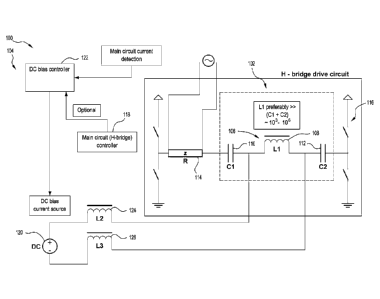
age
and use, and/or become affected by temperature, pressure, humidity and other
environmental variables.
CA 02944206 2016-09-28
WO 2015/157824
PCT/AU2015/050179
2
[0007] These factors have had the effect of limiting the effectiveness of
existing proximity detection systems in some work places. The electromagnetic
field
generated by these proximity detection systems can be weak, unreliable, and/or
prone to interruption or interference.
[0008] In transmitters used in existing proximity detection systems, it is
known
to use a variable inductor or a variable capacitor to compensate for any
changes in
the performance of the transmitter during set up and operation in a particular
environment. These variable inductors and capacitors are typically adjusted by
manual control or using a servomechanism. These solutions either involve field
intervention, or introduce additional complexity and consequent expense and
risk.
[0009] The present invention aims to address at least in part one or more
of
the disadvantages or problems described above, or at least to provide the
industry
with a useful choice.
[0010] In this specification, where a document, act or item of knowledge is
referred to or discussed, such a reference or discussion is not an admission
that the
document, act or item of knowledge or any combination thereof was at the
priority
date part of common general knowledge, or known to be relevant to an attempt
to
solve any problem with which this specification is concerned.
Summary of the invention
[0011] According to one aspect of the invention, there is provided a field
regulator for a resonant circuit, the resonant circuit including an inductor
coil around a
core, the field regulator including a DC bias circuit configured to apply a DC
bias
current to the inductor coil for regulating an electromagnetic field generated
by the
inductor.
[0012] The DC bias circuit can be used to selectively change the inductance
of
the inductor in the resonant circuit so as to maintain a consistent field
strength. In
particular, the DC bias current may be used to selectively change the natural
frequency of the resonant circuit so as to shift the resonant circuit towards
a desired
resonance point.
[0013] The variation in inductance is achieved without the need for an
additional control winding, by directly superimposing the DC bias current on
the
resonant circuit inductor.
[0014] Preferably, the field regulator includes a feedback control system
in
which the level of the applied DC bias current is determined based on a
current
measured in the resonant circuit.
CA 02944206 2016-09-28
WO 2015/157824
PCT/AU2015/050179
3
[0015] The field regulator therefore preferably includes:
a current detector for detecting a current flow of the resonant circuit, and
a bias current controller for controlling the DC bias current based on the
detected current flow of the resonant circuit.
[0016] A variation of the DC bias current may have the effect of modulating
the
resonant circuit response characteristics around a nominal circuit response
point, and
this can be used for adjusting the circuit resonance point to a target
resonance point.
[0017] To this end, the field regulator may be configured to adjust the DC
bias
current based on a resonant circuit response to an incremental change in the
DC
bias current. In particular, the bias current controller may be configured to
adjust the
DC bias current based on a detected change in the current flow of the resonant
circuit in response to an incremental change in the DC bias current.
[0018] The bias current controller may be configured to reduce the DC bias
current in response to a determination that the current flow of the resonant
circuit
decreases in response to an incremental increase in the DC bias current,
and/or that
the current flow of the resonant circuit increases in response to an
incremental
decrease in the DC bias current.
[0019] Further, the bias current controller may be configured to increase
the
DC bias current in response to a determination that the current flow of the
resonant
circuit increases in response to an incremental increase in the DC bias
current,
and/or that the current flow of the resonant circuit decreases in response to
an
incremental decrease in the DC bias current.
[0020] In theory, an increase in the current flow of the resonant circuit
in
response to an incremental increase in the DC bias current, and/or a decrease
in the
current flow of the resonant circuit in response to an incremental decrease in
the DC
bias current may indicate that the natural frequency is lower than the driving
frequency of the resonant circuit. Conversely, a decrease in the current flow
of the
resonant circuit in response to an incremental increase in the DC bias
current, and/or
an increase in the current flow of the resonant circuit in response to an
incremental
decrease in the DC bias current may indicate that the natural frequency is
higher
than the driving frequency of the resonant circuit.
[0021] The current detector preferably includes a current sensing resistor.
In
some embodiments, the current detector may include a hall effect device, a
magnetic
detection coil, or the like. The current detector may sample the current flow
of the
CA 02944206 2016-09-28
WO 2015/157824
PCT/AU2015/050179
4
resonant circuit at regular intervals. In some embodiments, the current
detector may
continuously detect the current flow of the resonant circuit. The bias current
controller
may determine a current flow of the resonant circuit by calculating an average
value
of the samples. Typically, the current detector is timed to sample the peak
value of
the current flow.
[0022] The bias current controller may be optionally coupled to a resonant
circuit controller which controls an alternating power supply to said resonant
circuit.
The bias current controller may determine appropriate sampling times based on
information from the resonant circuit controller.
[0023] The resonant circuit controller may include an H-bridge controller
for
controlling a driving frequency for driving the resonant circuit. Typically,
the H-bridge
controller includes a microprocessor for determining a driving frequency of
the H-
bridge.
[0024] The DC bias current source is preferably decoupled from high
voltages
of the resonant circuit. In a preferred embodiment, the field regulator
includes one or
more AC blocking inductors for decoupling the DC bias current source from
voltages
of the resonant circuit. Any suitable number of blocking inductors can be
used.
Preferably the field regulator includes a pair of blocking inductors connected
between
the resonant circuit and the DC bias current source. In particular, a blocking
inductor
may be connected to each terminal of the DC source. More particularly, the
inductance value of each blocking inductor may be at least an order of
magnitude
greater than that of the inductor of the resonant circuit. According to
another aspect
of the invention, there is provided a transmitter including:
a resonant circuit including an inductor coil around a core, and
a field regulator including a DC bias circuit for applying a DC bias current
to
the inductor coil for regulating an electromagnetic field generated by the
inductor.
[0025] The inductor may include a core of non-uniform permeability. The
permeability of the core preferably decreases from a centre portion towards an
outer
periphery. The core may include a plurality of voids evenly spaced along or
adjacent
an outer periphery of the core. More preferably, the voids may be elongate
slots
along an axial direction of the core.
[0026] Preferably, the resonant circuit includes blocking means to isolate
the
inductor coil such that the DC bias current only flows through the inductor
coil. In
other words, the blocking means advantageously prevent the DC bias current
from
affecting components of the resonant circuit other than the inductor coil.
CA 02944206 2016-09-28
WO 2015/157824
PCT/AU2015/050179
[0027] To this end, the resonant circuit may further include two or more
capacitors. Typically, the capacitors are connected in series to the inductor
coil. In
particular, a capacitor may be coupled in series to each terminal of the
inductor.
[0028] Preferably, the inductance to capacitance ratio (L/C ratio) for the
resonant circuit is in the range 1000 to 1,000,000. The inductor may have an
inductance in the region of 600pH. The pair of capacitors may have a combined
capacitance of approximately 3.3nF.
[0029] A current sensing resistor may be connected in series with one of
the
capacitors to enable detection of current flow through the inductor.
[0030] The resonant circuit may be powered by any suitable power source.
The resonant circuit may include an H-bridge for converting a DC signal from a
DC
power source to an AC signal for driving the resonant circuit. Alternatively,
an AC
signal from any suitable AC power source may be used to drive the resonant
circuit.
[0031] The transmitter may further include a H-bridge controller for
controlling
a driving frequency for driving the resonant circuit. The H-bridge controller
may be
separate to, or integrated with, the H-bridge.
[0032] In this form of the invention, the capacitors operate as blocking
capacitors for decoupling the DC bias current from the H-bridge and H-bridge
controller.
[0033] With the blocking inductors decoupling the DC bias current source
from
AC signals of the inductor, the configuration of the blocking capacitors and
inductors
allows for effective decoupling of the main and bias signals, enabling the DC
bias
current circuit to be used to regulate the operation of the inductor without
significantly
affecting other circuitry components.
[0034] The operating frequency of the resonant circuit may be between 50kHz
and 150kHz. Preferably, the operating frequency of the resonant circuit is
approximately 125kHz.
[0035] The transmitter may include a fault detection system for detecting a
fault condition when a required DC bias current adjustment exceeds operational
limits.
[0036] According to a further aspect of the invention, there is provided a
proximity detection system including a transmitter as described above.
[0037] The proximity detection system can include a plurality of
transmitters as
required to accommodate a particular application. Similarly, the proximity
detection
CA 02944206 2016-09-28
WO 2015/157824
PCT/AU2015/050179
6
system can include one or more receivers for detecting an electromagnetic
field
generated from a transmitter.
[0038] According to yet another aspect of the invention, there is provided
a
method of regulating a resonant circuit, the resonant circuit including an
inductor coil,
the method including the step of:applying a DC bias current to the inductor
coil for
regulating an electromagnetic field generated by the inductor.
[0039] The method may include the steps of:
setting the DC bias current to a predetermined value,
measuring the response of a current flow in the resonant circuit to an
incremental change in the DC bias current, and
determining whether a change to the DC bias current is required to achieve a
desired resonance point for the resonant circuit.
[0040] The method may include maintaining the DC bias current value in
response to a determination that no change is required.
[0041] The method may include:
increasing the DC bias current if the current flow of the resonant circuit
increases in response to an incremental increase in the DC bias current and/or
decreases in response to an incremental decrease in the DC bias current, and
decreasing the DC bias current if the current flow of the resonant circuit
increases in response to an incremental decrease in the DC bias current and/or
decreases in response to an incremental increase in the DC bias current.
[0042] The method may include adjusting the DC bias current by adjusting a
Pulse Width Modulation (PWM) duty cycle of the DC bias current.
[0043] The DC bias current can be used to selectively change the inductance
of the inductor in the resonant circuit so as to achieve and maintain a
desired field
strength. The variation in inductance is achieved without the need for an
additional
control winding, by directly superimposing the DC bias current on the resonant
circuit
inductor.
[0044] Reference throughout this specification to 'one embodiment' or 'an
embodiment' means that a particular feature, structure, or characteristic
described in
connection with the embodiment is included in at least one embodiment of the
present invention. Thus, the appearance of the phrases 'in one embodiment' or
'in an
embodiment' in various places throughout this specification are not
necessarily all
CA 02944206 2016-09-28
WO 2015/157824
PCT/AU2015/050179
7
referring to the same embodiment. Furthermore, the particular features,
structures, or
characteristic described herein may be combined in any suitable manner in one
or
more combinations.
Brief description of the drawings
[0045] The invention will now be further explained and illustrated by
reference
to the accompanying drawings in which:
[0046] Figure 1 is a schematic diagram of a transmitter according to an
embodiment of the present invention,
[0047] Figure 2 is a B-H curve illustrating the relationship between an
external
magnetising field and the induced magnetic flux density of the field
generating
antenna of the transmitter of Figure 1;
[0048] Figure 3 is a response curve illustrating the relationship between
the
resonant circuit current amplitude and the natural frequency of the resonant
circuit of
the transmitter of Figure 1;
[0049] Figures 4 is a flow diagram illustrating the operation of the
regulating
circuit of the transmitter of Figure 1; and
[0050] Figure 5 is a flow diagram illustrating the operation of the
regulating
circuit according to another embodiment of the invention.
Detailed description of the drawings
[0051] The transmitter 100 of Figure 1 forms part of a proximity detection
system (not shown). During operation, the transmitter 100 generates an
electromagnetic field for detection by one or more receivers (not shown) when
the
receivers are within range of the transmitter 100, allowing appropriate
warning
measures and/or collision avoidance measures.
[0052] The transmitter 100 includes a resonant circuit 102 and a field
regulating circuit 104 (field regulator). The resonant circuit 102 includes an
antenna
106 for generating the electromagnetic field during operation. The antenna 106
includes an inductor 108 having a cylindrical core of non-uniform permeability
(not
shown), and a single winding of inductor coil around the core. In particular,
the core
includes a plurality of axial elongate slots evenly spaced about an outer
periphery of
the core. The resonant circuit 102 also includes a pair of capacitors 110,
112. Each
capacitor 110, 112 is coupled in series to an opposite terminal of the
inductor 108 as
shown.
CA 02944206 2016-09-28
WO 2015/157824
PCT/AU2015/050179
8
[0053] The inductance to capacitance ratio (L/C) for the resonant circuit
102 is
in the range 1000 to 1,000,000. In a circuit tested, the inductor 108 has an
inductance of approximately 600pH, and the pair of capacitors 112, 110 has a
combined capacitance of approximately 3.3nF. The specific inductance and
capacitance values have been chosen to achieve a target resonant frequency of
around 125kHz.
[0054] The resonant circuit further includes a current sensing resistor 114
coupled in series with capacitor 110. The current sensing resistor 114 allows
measurement of the current flow in the inductor coil 108 to provide feedback
to the
regulating circuit 104. Positioning the current sensing resistor 114 between
an H-
bridge 116 and capacitor 110 ensures that the sensing resistor 114 and the
associated sensing circuitry are not subject to full resonance voltages across
the
inductor 108.
[0055] The H-bridge 116 of the resonant circuit 102 can be used to convert
a
DC signal from a DC power supply to an AC signal for driving the resonant
circuit
102. Alternatively, the H-bridge 116 can be used to modulate the frequency of
an AC
power source if required, such that an AC drive signal at a selected operating
frequency is applied to the resonant circuit 102.
[0056] It will be understood that, as an alternative to the H-bridge drive
described herein, the resonant circuit may be driven by an AC signal from any
other
suitable AC power source.
[0057] The resonant circuit 102 further includes an H-bridge controller 118
for
driving the H-bridge 116 at an appropriate driving frequency to generate the
required
AC signal. More particularly, the H-bridge controller 118 includes a
microprocessor
programmed to control a driving circuit, which drives the H-bridge at the
desired
driving frequency. As mentioned above, the operating frequency of the resonant
circuit is typically around 125kHz.
[0058] The field regulating circuit 104 includes a variable DC current
source
120 for applying a DC bias current to the inductor coil 108 via a bias current
circuit, in
order to regulate the electromagnetic field generated by the antenna 106, as
explained in further detail below.
[0059] The field regulating circuit 104 further includes a DC bias
controller 122
for controlling the level of DC bias current provided by the DC current source
120.
The operation of the bias current controller 122 will be explained in further
detail with
reference to Figure 4.
CA 02944206 2016-09-28
WO 2015/157824
PCT/AU2015/050179
9
[0060] In addition, the field regulating circuit 104 includes a pair of
inductors
124, 126 for decoupling the DC current source 120 from the high voltages of
the
resonant circuit 102. Each inductor 124, 126 is coupled in series to an
opposite
terminal of the DC current source 120 as shown in Figure 1. The inductance
value of
each blocking inductor 124, 126 is typically at least an order of magnitude
greater
than that of inductor 108. This advantageously prevents detuning of the
antenna 106
through the parallel blocking inductors 124, 126.
[0061] During operation of the transmitter 100, an input signal from the
power
supply is applied to the resonant circuit 102. The H-bridge controller 118 is
configured to drive the H-bridge 116 at an appropriate switching frequency to
convert
the input signal to an AC signal having a driving frequency of approximately
125kHz
and an amplitude of 24V. Such an AC signal is selected to drive the resonant
circuit
to operate in a resonant mode to generate an electromagnetic field having a
required
field strength and range.
[0062] As the transmitter 100 is moved into proximity to other metallic
objects,
the strength of the electromagnetic field generated by the transmitter 100 can
be
affected.
[0063] In order to control the electromagnetic field the regulating
circuit 104
applies a varying DC bias current through the inductor coil 108 so as to
compensate
for any changes in the electromagnetic field. The varying DC bias current is
thus
used to drive the resonant circuit 102 to operate as closely as possible to a
resonance point under varying external conditions of operation.
[0064] In particular, the bias current controller 122 can detect a change
in the
electromagnetic field by detecting a change in the current flow through the
inductor
108 as measured across the current sensing resistor 114 in response to an
incremental change to the DC bias current. The bias current controller 122
then
determines an appropriate DC bias current to be applied to the inductor coil
108
based on the detected change.
[0065] The capacitors 110, 112 are coupled in series to opposite terminals
of
the inductor coil 108 so as to isolate the H-bridge controller 118 from the DC
bias
current of the inductor 108. As previously mentioned, the inductors 124, 126
block
the DC current source 120 from high voltage AC signals across the inductor
108.
This solution provides effective decoupling of the main AC power signal and
the DC
bias signal so that the DC bias current can be used to regulate the
performance of
the antenna 106 without affecting operation of other circuitry components.
CA 02944206 2016-09-28
WO 2015/157824
PCT/AU2015/050179
[0066] The DC bias current can therefore be applied to the inductor coil
108 to
change the inductor core permeability and thus its inductance, thereby to
change the
natural frequency of the resonant circuit 102. By changing the natural
frequency to
closely match the drive frequency, a target resonant point for the resonant
circuit 102
can be achieved and maintained so as to establish a consistent operation of
the
transmitter 100.
[0067] The B-H curve (hysteresis curve) 200 of Figure 2 illustrates the
relationship between an external magnetising field H applied to the antenna
106 and
the induced magnetic flux density B of the antenna 106. The magnetic
permeability of
the inductor core, p = B/H, is represented by the slope of the curve 200. As
illustrated
by the curve 200, an increase in the external magnetising field H applied to
the
antenna 106 causes an increase in the induced magnetic flux density B, until a
state
of saturation is reached.
[0068] For effective operation, an operating region having a changing slope
on
the curve 200 and away from saturation is selected. For example, an operating
region around point A on the curve 200 is selected. At this operating region,
the slope
of the curve 200 can be changed by changing the external magnetising field H.
In this
manner, the magnetic permeability of the inductor 108 can be effectively
changed by
a change in the applied DC bias current.
[0069] In the device tested, the inductance and capacitance values of the
transmitter 100 were selected such that the natural frequency of the resonant
circuit
102 was as close as possible to the desired operating frequency of 125kHz. The
relationship between the natural frequency fn, the inductance L and the
capacitance
C of the resonant circuit 102 can be expressed using formula (1) below:
(1)
27NLC
[0070] An increase in the inductance L therefore causes a decrease in the
natural frequency fn of the resonant circuit 102, and vice versa.
[0071] When the antenna 106 is operating at point A as shown in Figure 2,
an
increase in the DC bias current has the effect of increasing the external
magnetising
field H, causing the operating point to shift slightly to the right side of
point A. As the
slope of the curve 200 decreases to the right of point A, the effective
permeability p
also decreases, thereby causing a decrease in inductance L and an increase in
the
natural frequency fn of the resonant circuit 102.
CA 02944206 2016-09-28
WO 2015/157824
PCT/AU2015/050179
11
[0072] Conversely, a decrease in the DC bias current has the effect of
decreasing the external magnetising field H, causing the operating point of
the
inductor 108 to shift slightly to the left of point A. As the slope of the
curve 200
increases to the left of point A, the effective permeability p also increases,
thereby
causing an increase in inductance L and hence an decrease in the natural
frequency
fn of the resonant circuit 102.
[0073] Determination of the prevalent natural frequency relative to the
driving
frequency can be achieved by perturbing the DC bias current marginally about
the
current value, and comparing the change in current in the resonant circuit 102
in
response to this tuning change.
[0074] As illustrated in the response curve 300 of Figure 3, the
horizontal axis
represents the driving frequency, as the ratio between driving frequency f and
the
resonant frequency fn of the resonant circuit 102. A peak resonant current
amplitude
for the resonant circuit 102 is achieved at point R of the curve 300, where
the
resonant frequency fn is equal to the driving frequency f of the resonant
circuit 102. In
practice, the resonant peak current amplitude is achieved when the natural
frequency
fn is as close as practically possible to the driving frequency f of the
resonant circuit
102, ie. ftzfn . When the resonant circuit 102 is operating at point B of the
curve 300,
the natural frequency fn is greater than the driving frequency f. When the
resonant
circuit 102 is operating at point C of the curve 300, the natural frequency fn
is lower
than the driving frequency f.
[0075] As previously discussed with reference to Figure 2, an increase in
the
DC bias current will decrease the permeability and inductance L of the
inductor 108,
hence increasing the natural frequency fr, of the resonant circuit 102.
Conversely, a
decrease in the DC bias current will decrease the natural frequency fn of the
resonant
circuit 102.
[0076] To determine whether the natural frequency fn of the resonant
circuit
102 is lower, approximately equal to, or greater than the driving frequency f,
a
change in the current flow I of the resonant circuit 102 in response to an
incremental
change in the input DC bias current is measured by the current sensing
resistor 114.
[0077] If the resonant circuit 102 is operating at point B of the curve
300, the
natural frequency fn is greater than the driving frequency f. When the input
DC bias
current is increased incrementally, the natural frequency fn also increases.
At point B,
an increase in the natural frequency fn will cause the operating point of the
resonant
circuit 102 to shift to the left side of point B, resulting in a corresponding
decrease in
the current lc of the resonant circuit 102. The reverse applies when the DC
bias
CA 02944206 2016-09-28
WO 2015/157824
PCT/AU2015/050179
12
current is decreased incrementally. Therefore, if the current ',of the
resonant circuit
102 decreases in response to an incremental increase to the DC bias current,
and
increases in response to an incremental decrease to the DC bias current, the
resonant circuit 102 is operating to the left side of the resonant point R on
the
response curve 300, and the natural frequency fn is greater than the drive
frequency
f. The bias controller 122 therefore decreases the input DC current to
decrease the
natural frequency fn until the natural frequency fn closely matches the drive
frequency.
[0078] Conversely, if the resonant circuit 102 is operating at point C of
the
curve 300, the natural frequency fn is lower than the driving frequency f.
When the
input DC bias current is increased incrementally, the natural frequency fn
also
increases. At point C, an increase in the natural frequency fn will cause the
operating
point of the resonant circuit 102 to shift to the left side of point C,
resulting in a
corresponding increase in the current lc of the resonant circuit 102. The
reverse
applies when the DC bias current is decreased incrementally. Therefore, if the
current lc of the resonant circuit 102 increases in response to an incremental
increase
to the DC bias current, and decreases in response to an incremental decrease
to the
DC bias current, the resonant circuit 102 is operating to the right side of
the resonant
point R on the response curve 300, and the natural frequency fn is lower than
the
drive frequency f. The bias controller 122 therefore increases the input DC
current to
increase the natural frequency fn until the natural frequency fn closely
matches the
drive frequency.
[0079] In practice, the DC bias current is typically adjusted by adjusting
the
PWM duty cycle of the DC bias current. Moreover, the measurement of the
current
flow of the resonant circuit 102 is carried out by sampling the current le at
regular
intervals and averaging the sampled values over a suitable period.
[0080] To allow effective adjustment of the natural frequency of the
resonant
circuit 102 about the desired operating frequency of 125kHz, the zero bias
resonance
point of the resonant circuit 102 is initially set at a set point below
125kHz, for
example at about 5% - 10% below 125kHz.
[0081] As discussed above, during setup and operation, the natural
frequency
of the resonant circuit 102 and hence the strength of the electromagnetic
field
generated by the antenna 106 can be affected by, for example, metallic objects
in the
surrounding environment. The operation process 400 by which the regulating
circuit
104 regulates the induced magnetic flux density B of the antenna 106 to
compensate
for the field changes will now be described with reference to Figure 4.
CA 02944206 2016-09-28
WO 2015/157824
PCT/AU2015/050179
13
[0082] At step 402, the bias current controller 122 sets the DC bias
current
provided by the DC current source 120 to a predetermined value. This
predetermined
value could be a factory setting or any suitable value as determined at
initial setup. At
the beginning of process 400, the current controller 122 initiates a sensing
mode
400A in which the controller 122 determines the general region of the response
curve
300 in which the resonant circuit 102 is operating (i.e, whether the natural
frequency
is higher, lower or generally equal to the drive frequency). The sensing mode
400A
includes steps 402 to 416.
[0083] At step 404, the current sensing resistor 114 measures the resonant
circuit current change (Ale) in response to an incremental increase in the DC
bias
current (lc).
[0084] At step 406, the current sensing resistor 114 measures the resonant
circuit current change (Ale) in response to an incremental decrease in the DC
bias
current ('DC).
[0085] At query step 408, the bias current controller 122 determines
whether
the DC bias current is too low. As previously discussed with reference to
Figure 3, an
increase in lc in response to an incremental increase in IDc and a decrease in
lc in
response to an incremental decrease in !pc indicates that the natural
frequency of the
resonant circuit is lower than the drive frequency (fn <f), and an increase in
!DC is
required to drive the natural frequency (fri) closer to the drive frequency.
If the DC
bias current is too low, process 400 proceeds to step 410. If not, it proceeds
to step
416.
[0086] At step 410, bias current controller 122 applies an incremental
increase
to the DC bias current. Typically, this is achieved by applying an incremental
increase
to the PWM duty cycle of the DC bias current, for example by 1%. At step 410,
the
controller 122 initiates the first adjustment mode 400B in which the DC bias
current is
increased until a resonant peak current amplitude is achieved for the resonant
circuit
102. The first adjustment mode 400B includes method steps 410 to 414.
[0087] At step 412, the current sensing resistor 114 measures the resonant
circuit current change (Ale) in response to the incremental increase in the DC
bias
current.
[0088] At query step 414, the bias current controller 122 determines
whether
the DC bias current is still too low. The DC bias current is too low if the
resonant
circuit current increases in response to an incremental increase in the DC
bias
current. Query step 414 is slightly different to query step 408 in that the
current
CA 02944206 2016-09-28
WO 2015/157824
PCT/AU2015/050179
14
controller 122 already knows that the resonant circuit 102 is operating in the
region in
which the natural frequency (fn) is lower than the drive frequency (i.e.
towards the
right side of the response curve 300 in Figure 3). Accordingly, it is not
necessary to
also determine the change in resonant circuit current (AI,) in response to an
incremental decrease in the DC bias current. If the DC bias current is too
low,
process 400 returns to step 410. If not, it proceeds to step 424.
[0089] At query step 416, the bias current controller 122 determines
whether
the DC bias current is too high. As previously discussed with reference to
Figure 3,
an decrease in I in response to an incremental increase in !pc, and an
increase in
in response to an incremental decrease in !pc indicates that the natural
frequency of
the resonant circuit is higher than the drive frequency (fn > f), and a
decrease in IDc is
required to drive the natural frequency JO closer to the drive frequency. If
the DC
bias current is too high, process 400 proceeds to step 418. If not, it
proceeds to step
424.
[0090] At step 418, bias current controller 122 applies an incremental
decrease
to the DC bias current. At step 418, controller 122 initiates a second
adjustment
mode 400C in which the DC bias current is decreased until a resonant peak
current
amplitude is achieved for the resonant circuit 102. The second adjustment mode
400C includes method steps 418 to 422.
[0091] At step 420, the current sensing resistor 114 measures the resonant
circuit current change (Ale) in response to the incremental decrease in the DC
bias
current.
[0092] At query step 422, the bias current controller 122 determines
whether
the DC bias current is still too high. As explained, the DC bias current is
too high if
the resonant circuit current increases in response to an incremental decrease
in the
DC bias current. Query step 422 is slightly different to query step 416 in
that the
current controller 122 already knows that the resonant circuit 102 is
operating in the
region in which the natural frequency (fn) is higher than the drive frequency
(i.e.
towards the left side of the response curve 300 in Figure 3). Accordingly, it
is not
necessary to determine the change in resonant circuit current (AL) in response
to an
incremental increase in the DC bias current. If the DC bias current is too
high,
process 400 returns to step 418. If not, it proceeds to step 424.
[0093] At step 424, a resonant current peak amplitude for the resonant
circuit
102 has been achieved and the bias current controller 122 implements a delay
for a
suitable time period, for example 60 seconds. From step 424, the controller
122
initiates a tracking mode 400D in which the achieved resonant current peak
CA 02944206 2016-09-28
WO 2015/157824
PCT/AU2015/050179
amplitude is maintained by making suitable incremental adjustments to the DC
bias
current value. The reason for the delay is that in the tracking mode, the
current
controller 122 samples the resonant circuit current at a lower frequency than
the
sensing and adjustment modes 400A, 400B and 400C.
[0094] At step 426, the current sensing resistor 114 measures the resonant
circuit current change (Ale) in response to the incremental increase in the DC
bias
current.
[0095] At query step 428, the bias current controller 122 determines
whether
the DC bias current is too low. The DC bias current is too low if the resonant
circuit
current increases in response to an incremental increase in the DC bias
current. If
the DC bias current is too low, process 400 proceeds to step 430. If not, it
proceeds
to step 432.
[0096] At step 430, the current controller 122 applies an incremental
increase
to the DC bias current.
[0097] At step 432, the current sensing resistor 114 measures the resonant
circuit current change (Ale) in response to the incremental decrease in the DC
bias
current.
[0098] At query step 434, the bias current controller 122 determines
whether
the DC bias current is too high. The DC bias current is too high if the
resonant circuit
current increases in response to an incremental decrease in the DC bias
current. If
the DC bias current is too high, process 400 proceeds to step 436. If not, it
returns to
step 424.
[0099] At step 436, the current controller 122 applies an incremental
decrease
to the DC bias current.
[0100] A typically operational value for the DC bias current IDc can range
from
50mA to 2000mA. In the embodiment described above, a typical current value for
IDc
is 350 to 400mA.
[0101] Figure 5 illustrates an alternative operating process 500 in which
the
regulating circuit 104 controls the DC bias current to achieve the desired
natural
frequency of the resonant circuit.
[0102] At step 502, the bias current controller 122 drives the DC current
source
120 to provide a DC bias current with a marginal fluctuation about a set
current value
IDC=
CA 02944206 2016-09-28
WO 2015/157824
PCT/AU2015/050179
16
[0103] At step 504, the change in the resonant circuit current in response
to
the DC bias current fluctuations are detected by way of the current sensing
resistor
114.
[0104] At step 506, the bias current controller 122 determines or estimates
the
natural frequency fn of the resonant circuit 102 relative to the drive
frequency based
on the current change detected at step 504 in the manner as previously
described.
[0105] At query step 508, the bias current controller 122 determines
whether
the natural frequency fn of the resonant circuit 102 is higher than an upper
limit of a
desired operating frequency range fup, for example 130kHz. If the natural
frequency fn
is higher than the upper limit fup, process 500 proceeds to step 512.
Alternatively, it
proceeds to step 510. In one example, the natural frequency may be estimated
by
measuring the attenuation of the resonant circuit current amplitude at the
operating
point of the resonant circuit 102 on the response curve 300.
[0106] At query step 510, the bias current controller 122 determines
whether
the natural frequency fn of the resonant circuit 102 is lower than a lower
limit of the
desired operating frequency range flow, for example 120kHz. If the natural
frequency
fn is lower than the lower limit f10, process 500 proceeds to step 514.
Alternatively, it
returns to step 502 without changing the set current value !DC.
[0107] At step 512, the bias current controller 122 reduces the set current
value IDc provided by the DC bias current source 120 by an incremental amount.
As
previously explained with reference to Figure 2, a decrease in the DC bias
current
causes the natural frequency of the resonant circuit 102 to decrease.
[0108] At step 514, the bias current controller 122 increases the set
current
value IDc provided by the DC bias current source 120 by an incremental amount.
As
previously explained with reference to Figure 2, an increase in the DC bias
current
causes the natural frequency of the resonant circuit 102 to also increase.
[0109] The field regulator 104 therefore provides a feedback control system
configured to detect a change in the electromagnetic field generated by the
resonant
circuit 102 during operation by detecting a change in the resonant circuit
current and
then automatically compensate for the change by adjusting the DC bias current.
[0110] The field regulator 104 thereby provides a cost effective means to
regulate the performance of the transmitter 100 without the need for manual
calibration or additional components such as servomechanisms.
[0111] In addition, during initial setup of the proximity detection system,
the
transmitters are mounted to various vehicles, machinery and equipment of a
work
CA 02944206 2016-09-28
WO 2015/157824
PCT/AU2015/050179
17
site. The metal of the vehicles, machinery and equipment can affect the
resonant
frequency of the respective resonant circuits 102. The field regulator 104 for
each
resonant circuit 102 automatically regulates the resonant frequency of the
resonant
circuit 102 after initial setup so that the strength and range of the
electromagnetic
field generated by each transmitter 100 can be maintained.
[0112] Moreover, the field regulator 104 can be used to assist the initial
tuning
process of the resonant circuit 102. During the initial tuning process,
appropriate
values must be determined for circuit capacitance and inductance to achieve a
particular resonant frequency for the resonant circuit. In cases where the
circuit
inductance is relatively high (which is the case for the embodiment described
above),
the matching capacitors must have very low capacitance values (e.g. in the nF
range). The tuning process involves selecting capacitors of standard value and
manufacturing tolerance, and then combining them in series and parallel to
achieve
the desired total effective capacitance. At the same time, consideration must
also be
given to the requirements of low tolerance, high voltage, low temperature
sensitivity,
low series resistance, and low nominal value for the combination of
capacitors.
Accordingly, it can often be very difficult to achieve the appropriate circuit
capacitance to match a specific circuit inductance for a target resonant
frequency. A
DC bias current provided by the field regulator of the invention can be used
to alter
the permeability and thus inductance of the resonant circuit such that an
appropriate
resonant frequency can be achieved even if it is not possible to achieve the
exact
circuit capacitance using available components.
[0113] Whilst the above example describes a field regulator 104 being used
in
relation to a transmitter 100 of a proximity detection system, a person
skilled in the
art will understand that the concept of the field regulator 104 may be used in
other
applications where it is desirable to tune and regulate the inductor
characteristics of a
resonant circuit (series or parallel), or generate and maintain oscillating
magnetic or
electric fields of a particular strength and range. Some examples include
active filters,
transmitters for public broadcast or point-to-point communication, metal or
ore
detection, carrier tracking with comparator and feedback control, generation
of AM
signals using resonance point de-tuning, and maintenance of a high SNR in FM
transmission by tracking the instantaneous transmission frequency.
Furthermore, the
field regulator may be used in AM, VHF, HF and LF applications.
[0114] The word 'comprising' and forms of the word 'comprising' as used in
this description do not limit the invention claimed to exclude any variants or
additions.
CA 02944206 2016-09-28
WO 2015/157824
PCT/AU2015/050179
18
[0115] Modifications and improvements to the invention will be readily
apparent to those skilled in the art. Such modifications and improvements are
intended to be within the scope of this invention.