Note: Descriptions are shown in the official language in which they were submitted.
CA 02944958 2016-105
WO 2015/155542 PCT/GB2015/051096
1
Low Pressure Sintering Powder
The invention relates to a sintering powder, a sintering
paste and film comprising the sintering powder, and a
sintered joint formed using the same.
Sintered joints provide an alternative to soldered joints. A
typical method of forming a sintered joint involves placing
a metal powder, often in the form of a powder compact,
between two work pieces to be joined and then sintering the
metal powder. The resulting atomic diffusion of the metal
atoms forms a bond between the two work pieces.
Metal nanopowders have been used to form sintered joints in
the electronics industry, and are considered to be useful
alternatives to lead-free soldering. The differing behaviour
between nanomaterials and the corresponding bulk material is
thought to be due to nanomaterials having a higher surface-
to-volume ratio.
Sintering powders containing silver nanoparticles are known.
Sintered joints formed by atomic diffusion of silver
nanoparticles can be processed at a temperature
significantly lower than the melting temperature of the bulk
and can also be used for high temperature applications. The
potential advantages, such as high temperature stability,
high electrical and thermal conductivity, and good
mechanical properties, make such sintering powders promising
candidates for die attachment applications. However, the
sintering temperatures of such sintering powders are still
too high for effective use in most electronics applications.
CA 02944958 2016-105
WO 2015/155542
PCT/GB2015/051096
2
Sintering temperatures may be reduced by applying an
external pressure during sintering. Pressure-assisted low-
temperature sintering of silver paste has been shown to be a
viable alternative to solder reflow as a die-attachment
method. The application of high pressure has been shown to
significantly lower the sintering temperature, and the
desired properties for die attachment can be achieved at a
relatively faster rate resulting in the formation of a
sintered joint within a few minutes. However, a large
external pressure makes automation of the process difficult.
Furthermore, application of a large external pressure may
result in damage to the work pieces.
It is known to dispense solder paste for a variety of
applications, but mostly as an alternative when wave solder
or screen printing is not possible. Solder paste can be
dispensed on a variety of surface mount applications on
printed circuit boards, integrated circuit packages, and
electrical component connectors. Typical problems of solder
paste include: dripping, skipped dots, and inconsistent
dispensing. Soft and hard solders are typically used in the
electronic industries for die attached and dispensing. The
soft solders are susceptible to fatigue failure under
thermal cycling conditions. On the other hand, hard solders
and glass matrix composites are used to enable devices to
run at higher junction temperatures, but their higher
elastic moduli and processing temperatures can generate high
mechanical stresses in devices, and these materials also
have relatively low thermal and electrical conductivities.
The present invention seeks to tackle at least some of the
problems associated with the prior art or at least to
CA 02944958 2016-10-05 2015/155542
PCT/GB2015/051096
3
provide a commercially acceptable alternative solution
thereto.
In a first aspect, the present invention provides a
sintering powder comprising:
a first type of metal particles having a mean longest
dimension of from 100 nm to 50 pm.
Each aspect or embodiment as defined herein may be combined
with any other aspect(s) or embodiment(s) unless clearly
indicated to the contrary. In particular, any features
indicated as being preferred or advantageous may be combined
with any other feature indicated as being preferred or
advantageous.
The term "sintering powder" as used herein may encompass a
powder capable of forming a sintered joint. Sintered joints
are formed by atomic diffusion of metal particles placed
between two work pieces to be joined. The term "sintering
powder" may encompass a particulate. The sintering powder
may comprise regular shaped particles (such as, for example,
spheres) or irregular shaped particles (such as, for
example, whiskers, plates, rods or flakes).
The term "capping agent" as used herein may encompass a
species that, when present on the surface of metal
particles, reduces agglomeration of the metal particles,
enables particle size control during powder production and
reduces particles' surface oxidation or other contamination.
The inventors have surprisingly found that the sintering
powder as described herein may be sintered at low
temperatures with the application of only very low pressure,
CA 02944958 2016-105
WO 2015/155542
PCT/GB2015/051096
4
typically substantially no pressure. As a result, formation
of a sintered joint between work pieces using the sintering
powder may occur with reduced damage to the work pieces. In
addition, since the application of high pressures is not
required, the formation of a sintered joint is simplified,
and may be more easily automated. Furthermore, in contrast
to nano-sized particles, agglomeration of the first type of
metal particles can be avoided by the use of only low
amounts of capping agent. Accordingly, in contrast to
sintering powders comprising nano-sized particles only, the
amount of residual organics contained in a resulting
sintered joint is reduced, thereby improving the mechanical
properties of the joint.
The first type of metal particles has a mean longest
dimension of from 100 nm to 50 pm. Mean longest dimensions
bigger than 50 pm may result in a low surface-to-volume
ratio, thereby requiring higher sintering temperatures
and/or pressures. Mean longest dimensions smaller than 100
nm may require unfavourable levels of capping agent.
Typically most of the particles of the first type of metal
particles have a longest dimension of from 100 nm to 50 pm,
more typically substantially all of the particles forming
the first type of metal particles have a longest dimension
of from 100 nm to 50 pm. When the particles forming the
particulate are spherical, the longest dimension will be the
diameter of the sphere. The mean longest diameters referred
to herein may be measured with a particle size analyser
using either a dynamic light scattering method or laser
scattering method.
The first type of metal particles may all comprise the same
metal. Alternatively, some of the particles may comprise
CA 02944958 2016-105
WO 2015/155542
PCT/GB2015/051096
different metals. In addition, individual particles may
comprise two or more different metals. The term "metal" as
used herein may encompass alloys or core-shell structures.
Accordingly, the particles may comprise one or more alloys
5 or alloys or core-shell structures of one or more metals.
Preferably, at least a portion of the first type of metal
particles are at least partially coated with a capping
agent. The use of a capping agent may help to reduce
agglomeration of the particles. Such agglomeration is
unfavourable, since it may increase the sintering
temperature of the sintering powder. Accordingly, the use of
a capping agent enables the formation of a sintered joint
between work pieces at lower temperatures and, therefore,
may help to reduce damage to a work piece caused by exposure
to high sintering temperatures. In addition, the use of a
capping agent may help to avoid degradation of the metal
such as, for example, damage caused by exposure of the metal
to air.
In this embodiment, the metal particles may be substantially
coated with the capping agent, or completely coated with a
capping agent. Increasing the coverage of the capping agent
on the metal particles may help to further reduce the
agglomeration of the metal particles and, therefore, further
reduce the sintering temperature. In addition, most of the
metal particles may be coated with the capping agent, or
substantially all of the metal particles may be coated with
a capping agent.
The capping agent preferably comprises a carboxylate and/or
amine functional group.
CA 02944958 2016-105
WO 2015/155542 PCT/GB2015/051096
6
The sintering powder preferably comprises up to 5 wt%
capping agent, more preferably from 0.1 to 3 wt% capping
agent, even more preferably about 0.5 wt% capping agent. The
term "wt%" used in this regards is based on the total weight
of the sintering powder. If the sintering powder comprises
more than 5 wt% capping agent, then higher temperatures may
be required to melt the capping agent prior to sintering.
Furthermore, the amount of organics contained in the
resulting sintered joint may increase. If the sintering
powder comprises less than 0.1 wt% capping agent, then the
capping agent may not adequately cover the surface of the
metal. This may result in an increase in agglomeration of
the particles and, therefore, an increase in the sintering
temperature. The combination of the size of the first type
of metal particles and the low levels of capping agent may
result in a combination of a strong resulting joint, low
required sintering temperatures and pressures and reduced
agglomeration of the particles.
The first type of metal particles preferably has a mean
longest diameter of from 100 nm to 20 pm, more preferably
from 150 nm to 15 pm, even more preferable from 200 nm to 10
pm.
The first type of metal particles preferably has a 1J50 value
(i.e. the value of the particle diameter at 50% in the
cumulative distribution) of from 1 to 3 pm. This may provide
particularly favourable sintering characteristics. The 1J50
may be measured with a particle size analyser using either a
dynamic light scattering method or laser scattering method.
The first type of metal particles preferably has a tap
density of from 3.5 to 5.5 g/cc. The tap density may be
CA 02944958 2016-105
WO 2015/155542
PCT/GB2015/051096
7
measured under the standard procedure using a tap density
meter. Higher tap densities indicate presence of less degree
of agglomeration of the metal particles prior to sintering.
The sintering powder may comprise a second type of metal
particles having a mean longest dimension of less than 100
pm, wherein the second type of metal particles are at least
partially coated with a capping agent. The combination of
the first and second types of metal particles increases the
contact points of the particles forming the sintering
powder. This may result in better sintering and also an
improved morphology of the powder. Accordingly, the
thermocycling properties of a joint formed using such a
powder are improved. In addition, the larger first type of
particles typically require only low levels of capping
agent. Accordingly, in comparison to a sintering powder
comprising only nano-sized particles, the total amount of
capping agent in the sintering powder may be reduced,
thereby minimising the existence of residual organics in any
formed joint. As a result, the thermoconductivity and high
temperature properties, such as thermocycling, are improved.
Typically most of the particles of the second type of metal
particles have a longest dimension of less than 100 pm, more
typically substantially all of the particles forming the
second type of metal particles have a longest dimension of
less than 100 pm.
In one embodiment, the second type of metal particles
preferably has a mean longest dimension of from 1 to 100 nm,
preferably from 5 to 75 nm. In this embodiment, typically
most of the particles of the second type of metal particles
have a longest dimension within these ranges, more typically
substantially all of the particles forming the second type
CA 02944958 2016-10-05
WO 2015/155542 PCT/GB2015/051096
8
of metal particles have a longest dimension within these
ranges.
The sintering powder preferably comprises from 1 to 19 wt%
of the first type of metal particles and from 81 to 99 wt%
of the second type of metal particles, preferably from 5 to
wt% of the first type of metal particles and from 85 to
95 wt% of the second type of metal particles. Such ranges
are particularly suitable for providing the combination of
10 improved thermoconductivity and thermocycling properties,
and low sintering temperature. In a preferred embodiment,
the particulate comprises about 10 wt% of the first type of
particles and about 90 wt% of the second type of particles
15 The first type of metal particles and/or second type of
metal particles preferably comprises silver or an alloy or
alloys or core-shell structures thereof. Silver has
excellent electrical and thermal conductivity, and is
therefore capable of forming a sintered joint with high
electrical and/or thermal conductivity. Accordingly, the use
of silver metal makes the sintering powder particularly
suitable for use in electronics applications, such as die
attachment and microelectronic packaging. Suitable silver
alloys include, for example, AgSn, AgPd, AuAg, AgCu and
AgNi. The metal particles may comprise core-shell structures
of silver coated particles such as, for example, silver
coated copper, silver coated nickel, silver coated CuNi,
silver coated CuNiZn and silver coated BN.
The capping agent of the first type of metal particles may
be inorganic and/or organic. Examples of organic capping
agents include polymers and ligands. Preferably the capping
agent of the first type of metal particles comprises an
CA 02944958 2016-105
WO 2015/155542
PCT/GB2015/051096
9
amine and/or a carboxylate functional group. Such capping
agents may form a weak bond with the metal particles.
Accordingly the temperature required to break the bonding
may be reduced, which may help to reduce the sintering
temperature. Capping agents that comprise an acid functional
group are particularly preferred in this regard.
Preferably the capping agent of the first type of metal
particles comprises a straight chain carboxylic acid (C6 to
C22) or a branched chain aliphatic carboxylic acid. One
preferred example is oleic acid. Oleic acid forms a
particularly weak bond with metal particles. In addition,
oleic acid is particularly effective at reducing
agglomeration of metal particles.
The capping agent of the second type of metal particles may
be inorganic and/or organic. Examples of organic capping
agents include polymers and ligands. Preferably the capping
agent of the second type of metal particles comprises an
amine and/or a carboxylate functional group. Such capping
agents may form a weak bond with the metal particles.
Accordingly the temperature required to break the bonding
may be reduced, which may help to reduce the sintering
temperature. Capping agents that comprise an amine
functional group are particularly preferred in this regard.
Preferably the capping agent of the second type of metal
particles comprises a straight chain alkylamine (C6 to C18)
or a branched chain aliphatic alkylamine. One preferred
example is octylamine. Octylamine forms a particularly weak
bond with metal particles. In addition, octylamine is
particularly effective at reducing agglomeration of metal
particles.
CA 02944958 2016-10-05
WO 2015/155542
PCT/GB2015/051096
In a particularly preferred embodiment, the sintering powder
comprises:
from 1 to 10 wt % of a first type of metal particles
5 having a mean longest dimension of from 100 nm to 20 pm, the
metal particles at least partially coated with an oleic acid
capping agent; and
from 90 to 99 wt% of a second type of metal particles
having a mean longest dimension of from 5 to 75 nm, wherein
10 the second type of metal particles are at least partially
coated with an octylamine capping agent.
In a further aspect, the present invention provides a
sintering powder comprising:
metal particles having a mean longest dimension of less
than 10 pm,
wherein at least some of the metal particles are at least
partially coated with a capping agent.
Such a sintering powder may be sintered at particularly low
temperatures with the application of only very low pressure,
typically substantially no pressure. As a result, formation
of a sintered joint between work pieces using the sintering
powder may occur with reduced damage to the work pieces. In
addition, since the application of high pressures is not
required, the formation of a sintered joint is simplified,
and may be more easily automated.
Preferably the metal particles have a mean longest dimension
of from 1 to 100 nm, more preferably from 5 to 75 nm, even
more preferably from 5 to 65 nm. Such mean longest
dimensions may be particularly effective at providing a high
surface-to-volume ratio. Metal particles having a mean
CA 02944958 2016-10-05
WO 2015/155542
PCT/GB2015/051096
11
longest dimension smaller than 1 nm may be difficult to
handle and may also be more susceptible to degradation.
The metal particles may have a mean longest dimension of
from 500 nm to 5 pm. Larger particle sizes may require less
capping agent. Accordingly, due to the reduction in residual
organics in the resulting joint, the resistivity is much
lower. In one aspect of the present invention, the metal
particles have a mean longest diameter of from 100 nm to 10
pm, preferably from 500 nm to 3 pm and comprise less than 3
wt% capping agent, typically about 0.5 wt% capping agent.
When the metal particles have a mean longest dimension in
the ranges specified above, typically most of the particles
have a longest dimension within the range, more typically
substantially all of the particles have a longest dimension
within the range.
The particulate typically exhibits heterogeneous particle
sizes. For example, the difference between the mean longest
dimension of the largest 10 % of the particles and mean
longest dimension of the smallest 10 % of the particles may
be greater than 20 nm, typically greater than 30 nm, even
more typically greater than 60 nm, still even more typically
from 60 to 150 nm. The heterogeneous particle sizes may help
to reduce the sintering temperature of the sintering powder,
presumably due to the large point of contact between the
particles. In addition, such heterogeneous sizes may help to
increase the packing fraction.
The capping agent may be inorganic and/or organic. Examples
of organic capping agents include polymers and ligands.
Preferably the capping agent comprises an amine and/or a
CA 02944958 2016-10-05 2015/155542
PCT/GB2015/051096
12
carboxylate functional group. Such capping agents may form a
weak bond with the metal particles. Accordingly the
temperature required to break the bonding may be reduced,
which may help to reduce the sintering temperature. Capping
agents that comprise an amine functional group are
particularly preferred in this regard.
Preferably the capping agent comprises straight chain
alkylamine (C6 to C18) or a branched chain aliphatic
alkylamine. One preferred example is octylamine. Octylamine
forms a particularly weak bond with metal particles. In
addition, octylamine is particularly effective at reducing
agglomeration of metal particles.
The metal preferably comprises silver or an alloy or alloys
or core-shell structures thereof. Silver has excellent
electrical and thermal conductivity, and is therefore
capable of forming a sintered joint with high electrical
and/or thermal conductivity. Accordingly, the use of silver
metal makes the sintering powder particularly suitable for
use in electronics applications, such as, for example, die
attachment and microelectronic packaging. Alternatively, the
metal may comprise other metals such as, for example, copper
and gold.
In a further aspect, the present invention provides a
sintering powder comprising:
a particulate having a mean longest diameter of less
than 10 pm, wherein at least some of the particles forming
the particulate comprise a metal at least partially coated
with a capping agent.
CA 02944958 2016-10-05
WO 2015/155542
PCT/GB2015/051096
13
In a further aspect, the present invention provides A
sintering powder comprising:
a particulate having a mean longest diameter of less
than 10 pm, wherein at least some of the particles forming
the particulate comprise a metal at least partially coated
with a capping agent, wherein the particulate comprises a
first type of particles having a longest diameter of from
greater than 100 nm to 50 pm and a second type of particles
having a longest diameter of from 1 to 100 nm, wherein the
particulate comprises from 5 to 15 wt% of the first type of
particles and from 85 to 95 wt% of the second type of
particles.
In a further aspect, the present invention provides a
sintered joint formed using the sintering powder as
described herein. Such a sintered joint may exhibit
particularly high strength and/or particularly high
electrical and thermal conductivity. Furthermore, the
sintered joint may exhibit very little change in shear
strength following thermal shock, typically substantially no
change in shear strength.
In a further aspect, the present invention provides an LED
(light-emitting diode), MEMS (microelectromechanical
system), OLED (organic light-emitting diode) or PV cell
(photovoltaic cell) comprising the sintered joint described
herein.
In a further aspect the present invention provides a
sintering paste comprising:
the sintering powder as described herein;
a binder;
a solvent; and
CA 02944958 2016-10-05 2015/155542
PCT/GB2015/051096
14
optionally a rheology modifier and/or an organosilver
compound and/or an activator and/or a surfactant and/or
wetting agent and/or hydrogen peroxide or organic peroxides.
The paste may be printable and/or dispensable and/or
jettable and/or pin transferable. The paste may have
viscosity and flow characteristics particularly favourable
for dispensing, meaning that the paste may be used as a one-
to-one replacement for solders.
Compared to sintering pastes known in the art, the sintering
paste of the present invention exhibits high stability at
room temperature. This means that low temperature storage of
the sintering paste is not required. This is a particularly
important advantage of the sintering paste of the present
invention.
The binder and/or solvent are typically selected so that
they are able to be removed from the paste (for example by
evaporation and/or burn out) at a temperature below the
targeted sintering temperature of the sintering powder. This
may help to promote near complete sintering of the metal
particles. When organic material remains in the joint during
sintering, inadequate sintering of the metal particles may
occur. This may result in a weak sintered joint.
The binder may serve to bind the paste together so that it
is easier to handle and position accurately in the location
of a desired sintered joint. Examples of suitable binders
include, but are not restricted to, thermoplastic polymers,
such as, for example, poly(methyl methacrylate), polyamides,
polyethylene, polypropylene, polystyrene; or thermosetting
polymers, such as, for example, polyurethanes,
CA 02944958 2016-105
WO 2015/155542
PCT/GB2015/051096
polycyanurates, epoxy resin, polyimides, melamine resin and
bismaleimide resin. Particularly preferred examples include
hydroxypropylmethylcellulose, triacetin and polyvinyl
acetate. Preferably the binder comprises an epoxy-based
5 resin. Epoxy-based resin may be particularly effective at
binding the paste together so that the paste is easier to
handle and may be easier to position accurately in the
location of a desired sintered joint. Furthermore, the use
of epoxy resin may result in the formation of a stronger
10 joint prior to sintering, meaning that there is no
requirement to hold together the work pieces to be joined
prior to sintering. The use of epoxy resin is particularly
advantageous when the capping agent comprises an amine
functional group. In this case, the amine acts as a hardener
15 forming a cross-linked structure. This may result in a
particularly strong joint prior to sintering.
The solvent preferably comprises a monoterpene alcohol
and/or a glycol and/or glycol ether, preferably terpineol
and/or diethylene glycol mono-n-butyl ether. Monoterpene
alcohol and/or a glycol ether may be particularly effective
at dispersing the metal particles within the paste,
resulting in a homogeneous distribution of metal particles
in the matrix of organic components with reduced cluster
aggregation and/or agglomeration. The use of monoterpene
alcohol and/or a glycol ether may serve to increase the
flow-ability and printer-ability of the sintering paste.
A rheology modifier may be added to control the viscosity of
the paste. Examples of suitable rheology modifiers include,
but are not restricted to, short or long chain (C = 2 to 30)
carboxylic acids or di-carboxylic acids or hydroxyl
carboxylic acids, for example lauric acid, stearic acid,
CA 02944958 2016-10-05 2015/155542
PCT/GB2015/051096
16
neodecanoic acid, stearic acid, oleic acid, oxalic acid,
malonic acid, succinic acid, adipic acid, maleic acid,
citric acid, lactic acid or short or long chain (C = 2 to
30) amines, for example, butyl amine, hexyl amine, octyl
amine, dodecyl amine, hexadecyl amine, Thixcin R and
Crayvallac Super, or combinations of two or more thereof.
During sintering, the organosilver compound may break down
to metallic silver, which may increase the thermal
conductivity of the sintered joint. In addition, the
presence of the organosilver compound increases the wetting
of the paste to the joint interface. The organosilver
compound may comprise one or more of short or long chain
carboxylic acids (C = 1 to 30), such as, for example, silver
stearate, silver palmitate, silver oleate, silver laurate,
silver neodecanoate, silver decanoate, silver octanoate,
silver hexanoate, silver lactate, silver oxalate, silver
citrate, silver acetate and silver succinate. In some
embodiments, the organosilver compound may be omitted.
An activator may be added to remove any metal oxide that may
be present from the surface being printed and/or to remove
any oxides that may be present in the sintering powder. Aryl
or alkyl carboxylic acids may be used as activators, such
as, for example, one or more of adipic acid, succinic acid
and glutaric acid.
A surfactant may be added to the sintering paste to help
disperse the sintering powder in the sintering paste.
Examples of suitable surfactants include, but are not
restricted to, Disperbyk 163, IGEPAL CA-630, lauryl
glucoside and TritonX 100.
CA 02944958 2016-10-05 2015/155542 PCT/GB2015/051096
17
The sintering paste preferably further comprises a peroxide.
Examples of suitable peroxides include, but are not
restricted to, hydrogen peroxide or organic peroxides, such
as, for example, tertiary-butyl hydroperoxide and tertiary-
butyl peroxy-2-ethylhexanoate. Peroxide introduces oxygen
into the paste, which may aid sintering of the paste beneath
the die area in a die attach method. The oxygen may also
enable sintering of the metal particles under an inert
atmosphere, such as, for example, a nitrogen atmosphere. The
sintering paste preferably comprises up to 3 wt.% hydrogen
peroxide or organic peroxides, preferably from 0.5 to 2 wt.%
hydrogen peroxide or organic peroxides, more preferably from
0.7 to 1.8 wt.% hydrogen peroxide or organic peroxides.
Liquid peroxides are preferred to control rheology and
silver settling.
The sintering paste preferably comprises:
from 1 to 15 wt% binder; and/or
from 1 to 30 wt% solvent; and/or
up to 5 wt% rheology modifier; and/or
up to 10 wt% an organosilver compound; and/or
up to 2 wt% activator; and/or
up to 6 wt% surfactant; and/or
up to 2 wt% hydrogen peroxide or organic peroxides.
Binder and/or solvent contents within these ranges may help
to provide the sintering paste with particularly desirable
flow-ability and printer-ability. Preferably the sintering
paste comprises from 2 to 8 wt%, binder. In one embodiment
the sintering paste comprises about 4.5 wt% binder.
Preferably the sintering paste comprises from 5 to 30 wt%,
solvent. In one embodiment the sintering paste comprises
about 26 wt% solvent. The sintering paste may comprise 0 to
CA 02944958 2016-10-05
WO 2015/155542
PCT/GB2015/051096
18
wt% rheology modifier and/or 0 to 2 wt% activator and/or 0
to 6 wt% surfactant and/or 0 to 2 hydrogen peroxide or
organic peroxides. The sintering paste may comprise from 62
to 90 wt% sintering powder. The sintering powder may form
5 the balance of the sintering paste.
In a further aspect the present invention provides a
sintering paste comprising:
the sintering powder as disclosed herein;
an organosilver compound;
a solvent; and
optionally an activator and/or rheology modifier and/or
surfactant and/or hydrogen peroxide or organic peroxides.
During sintering, the organosilver compound may break down
to metallic silver, which may increase the thermal
conductivity of the sintered joint. In addition, the
presence of the organosilver compound increases the wetting
of the paste to the joint interface. The organosilver
compound may comprise one or more of short or long chain
carboxylic acids (C = 1 to 30), such as, for example, silver
stearate, silver palmitate, silver oleate, silver laurate,
silver neodecanoate, silver decanoate, silver octanoate,
silver hexanoate, silver lactate, silver oxalate, silver
citrate, silver acetate and silver succinate. In some
embodiments, the organosilver compound may be omitted.
The sintering paste preferably further comprises a fatty
acid and/or wetting agent, preferably one or more of: short
or long chain (C = 2 to 30) carboxylic acids or di-
carboxylic acids or hydroxyl carboxylic acids, more
preferably lauric acid, stearic acid, neodecanoic acid,
stearic acid, oleic acid, oxalic acid, malonic acid,
CA 02944958 2016-10-05 2015/155542 PCT/GB2015/051096
19
succinic acid, adipic acid, maleic acid, citric acid or
lactic acid; or short or long chain (C = 2 to 30) amines,
more preferably butyl amine, hexyl amine, octyl amine,
dodecyl amine or hexadecyl amine; or surfactants, more
preferably triton X100, IGEPAL CA-630 or lauryl glucoside.
The presence of fatty acids helps to bind the paste
together. In other words, the presence of a fatty acid
avoids the need for a separate binder, such as the epoxy
based resin binder discussed above. Accordingly, the total
amount of organics in the paste is less, resulting in a
stronger final joint.
The sintering paste preferably further comprises a peroxide.
Examples of suitable peroxides include, but are not
restricted to, hydrogen peroxide or organic peroxides, such
as, for example, tertiary-butyl hydroperoxide and tertiary-
butyl peroxy-2-ethylhexanoate. Peroxide introduces oxygen
into the paste, which may aid sintering of the paste beneath
the die area in a die attach method. The oxygen may also
enable sintering of the metal particles under an inert
atmosphere, such as, for example, a nitrogen atmosphere. The
sintering paste preferably comprises up to 3 wt.% hydrogen
peroxide or organic peroxides, preferably from 0.5 to 2 wt.%
hydrogen peroxide or organic peroxides, more preferably from
0.7 to 1.8 wt.% hydrogen peroxide or organic peroxides.
Liquid peroxides are preferred to control rheology and
silver settling.
The sintering paste may comprise a film forming agent such
as, for example, a polyamide, polyisobutylene, polyamide wax
rheology modifier and castor oil based thixotropes.
CA 02944958 2016-10-05
WO 2015/155542
PCT/GB2015/051096
Preferably the sintering paste is substantially resin free,
more preferably completely resin free. The presence of resin
may reduce the thermal and electrical conductance of the
silver. The solvent preferably comprises a monoterpene
5 alcohol and/or a glycol and/or glycol ether, more preferably
a terpineol and/or diethylene glycol mono-n-butyl ether.
The sintering paste preferably comprises:
from 1 to 30 wt% solvent; and/or
10 up to 50 wt% organosilver compound, preferably from 0.1
to 25 wt%, more preferably from 0.1 to 10 wt%, even more
preferably from 0.1 to 9 wt%; and/or
up to 5 wt% rheology modifier; and/or
up to 2 wt% activator; and/or
15 up to 6 wt% surfactant; and/or
up to 2 wt% hydrogen peroxide or organic peroxides.
The sintering paste may comprise 0 to 5 wt% rheology
modifier and/or 0 to 2 wt% activator and/or 0 to 6 wt%
20 surfactant and/or 0 to 2 hydrogen peroxide or organic
peroxides. The sintering powder may form the balance of the
sintering paste.
In a further aspect the present invention provides a
sintering film comprising the sintering powder as described
herein and a binder. The film may be applied at the wafer
level, die level, package/substrate level, and/or module
level. Such a film may be obtained, for example, by printing
the sintering paste as described herein onto a polyester
sheet, heating the paste to at least partially remove the
solvent and form a film, and then removing the film from the
polyester sheet. The film as described herein is especially
advantageous since it can be transferred on the die by
CA 02944958 2016-105
WO 2015/155542 PCT/GB2015/051096
21
simply pressing the die on to the film at slightly elevated
temperature. Transferred film is an alternate application
method, beneficially offered in certain situations. The film
may be formed on a polymeric, glass, metal or ceramic
substrate or directly on a wafer. The film may be on a
polymeric substrate comprising polyester. The film may be
formed on a polymeric substrate, wherein the polymeric
substrate comprises a release coating. The film may be
produced by applying the paste compositions by printing or
casting of the material. The film may be produced by
printing in a continuous layer. Alternatively, the film may
be produced by printing to form an array of discrete shapes.
In a further aspect the present invention provides a method
of die attachment comprising:
(i) placing the sintering film described herein between
a die and a substrate to be joined; and
(ii) sintering the sintering film,
wherein the sintering is carried out without the application
of pressure.
This "low pressure" or "pressureless" sintering is
particularly advantageous, since it may make automation of
the process simpler. Furthermore, damage to the work pieces
may be reduced. Further advantages over methods employing
pressured sintering include: shorter time required for die-
placement (high UPH), low-pressure requirement for placement
(highly advantageous for processing thin wafers),
compatibility with commercial die-bonder and sintering in
external heating equipment (batch process to improve UPH).
The sintering is preferably carried out at a temperature of
from 150 to 400 C for up to 120 minutes. Such conditions
CA 02944958 2016-105
WO 2015/155542
PCT/GB2015/051096
22
may result in particularly effective sintering of the
sintering film while avoiding damage to the work pieces.
Step preferably (i) comprises:
(a) applying the sintering film to the die to form an
assembly having a die side and a sintering film side; and
(b) contacting the film side of the assembly with the
substrate.
Such a step may make automation of the process simpler, and
may be carried out, for example, by the use of a stamp.
Step (a) is preferably carried out at a temperature of from
to 400 C and a pressure of from 0.1 to 5 MPa for from
15 0.1 to 60 seconds. Such conditions may result in
particularly effective application of the sintering film
while avoiding damage to the die.
Step (b) is preferably carried out at a temperature of from
15 to 400 C and a pressure of from 0.1 to 40 MPa for from
0.1 to 60 minutes. Such conditions may result in
particularly effective contacting of the die to the
substrate while avoiding damage to the die or substrate.
In a further aspect, the present invention provides a method
of die attachment comprising:
(i) placing the sintering film described herein between
a die and a substrate to be joined; and
(ii) sintering the sintering film,
wherein the sintering is carried out while applying a
pressure of from 0.1 to 40 MPa.
CA 02944958 2016-105
WO 2015/155542
PCT/GB2015/051096
23
In a further aspect, the present invention provides a method
of wafer bonding comprising:
(i) placing the sintering film described herein between
two or more wafers to be joined; and
(ii) sintering the sintering film,
wherein the sintering is carried out without the application
of pressure.
In a further aspect, the present invention provides a method
of transferring a sintering film to a component, comprising:
applying the sintering film described herein to a
substrate to form an assembly having a sintering film side
and a substrate side;
contacting the sintering film side of the assembly with
a component;
heating the assembly to a temperature of from 50 to 200
C;
applying a pressure of from 1 to 5 MPa to the assembly
for from 0.1 seconds to 60 minutes; and
separating the substrate from the sintering film.
The substrate may be polymeric. The sintering film may be
substantially the same size as the component. The component
may be an LED.
In a further aspect the present invention provides a method
for die-attachment, comprising: applying the sintering film
described herein to a substrate; placing a die on the film
to form an assembly; applying a pressure of less than 2 MPa
to the assembly; and sintering the assembly at a temperature
of 100 to 400 C for 0.1s to 5 minutes, applying a pressure
of less than 3 MPa. The same assembly may be further
CA 02944958 2016-105
WO 2015/155542 PCT/GB2015/051096
24
sintered at a temperature of 175 to 400 C in a pressureless
manner using variety of processes and equipment that provide
appropriate degree of heat to initiate and complete
sintering.
In a further aspect the present invention provides a method
for die-attachment attachment, comprising: applying the
sintering film described herein to a substrate; placing a
die on the film to form an assembly; applying a pressure of
less than 5 MPa to the assembly; and sintering the assembly
at a temperature of 100 to 400 C for 0.1s to 60 minutes,
applying a pressure of less than 40 MPa. The same assembly
may be further sintered at a temperature of 175 to 400 C in
a pressureless manner using variety of processes and
equipment that provide appropriate degree of heat to
initiate and complete sintering.
In a further aspect the present invention provides a method
for die-attachment attachment, comprising: applying the
sintering film described herein on a back side of a wafer;
dicing the wafer to form a plurality of die; placing at
least one die on a substrate to form an assembly; applying a
pressure of more than 1 MPa to the assembly; and sintering
the assembly at a temperature of 100 to 400 C for 0.1s to
60 minutes. The same assembly may be further sintered at a
temperature of 175 to 400 C in a pressureless manner using
variety of processes and equipment that provide appropriate
degree of heat to initiate and complete sintering.
In a further aspect the present invention provides a method
for wafer bonding, comprising: applying the sintering film
described herein on a back side of a wafer; placing one more
CA 02944958 2016-105
WO 2015/155542
PCT/GB2015/051096
same or different types of wafer on the sinterable Ag film
containing wafer to form an assembly; applying a pressure of
more than > 0.1 MPa to the assembly; and sintering the
assembly at a temperature of 100 400 C for 0.25s to 120
5 minutes. The same assembly may be further sintered at a
temperature of 175 to 400 C in a pressureless manner using
variety of processes and equipment that provide appropriate
degree of heat to initiate and complete sintering.
10 In a further aspect the present invention provides a method
for wafer bonding, comprising: applying the sintering film
on a back side of a wafer; placing one more same or
different types of wafer on the sintering film containing
wafer to form an assembly; applying a pressure of less than
15 40 MPa to the assembly; and sintering the assembly at a
temperature of 100 to 400 C for 0.25s to 120 minutes. The
same assembly may be further sintered at a temperature of
175 to 400 C in a pressureless manner using variety of
processes and equipment that provide appropriate degree of
20 heat to initiate and complete sintering.
In a further aspect the present invention provides the use
of the sintering powder as described herein or the sintering
paste or film as described herein in a method selected from:
25 die attachment (e.g. chip-to-board, chip-to-substrate, chip-
to-heat sink, chip-to-fixture), wafer-to-wafer bonding (e.g.
chip-to-heat sink), reflective layer printing, hermetic and
near hermetic sealing (for example for packages and
perimeter seals), the production of interconnect lines (for
example circuitry, pads), via filling in semiconductor
devices and substrates, and flip-chip and wafer bumping.
CA 02944958 2016-10-05 2015/155542 PCT/GB2015/051096
26
In a further aspect the present invention provides a method
of manufacturing a sintered joint comprising the steps:
providing the sintering powder as described herein or
the sintering paste or film as described herein in the
vicinity of two or more work pieces to be joined; and
heating the sintering powder or sintering paste or film
to at least partially sinter the metal.
Advantageously, the heating step may be carried out at
atmospheric pressure. The sintering powder or sintering
paste or film may be placed in the vicinity of the work
piece under low pressure (typically 1-5 MPa for 0.1 to 60
seconds at a temperature of about 175 to 250 C).
The heating step is preferably carried out at a temperature
of at least 140 C, more preferably from 150 to 350 C, even
more preferably from 160 to 300 C. Temperatures lower than
140 C may not result in adequate sintering of the particles
in the sintering powder and/or may not result in adequate
removal of the organics by evaporation and/or burn out.
Temperatures higher than 350 C may result in damage to the
work pieces.
In a further aspect the present invention provides a method
of manufacturing the sintering powder as described herein
comprising the steps:
providing a metal salt solution;
contacting the metal salt solution with a capping
agent; and
precipitating metal particles at least partially coated
with the capping agent.
CA 02944958 2016-10-05 2015/155542
PCT/GB2015/051096
27
The precipitated metal particles may be recovered from the
solvent, for example by filtering. An example of the metal
salt solution is a metal nitrate solution.
The precipitating step may be carried out using a reducing
agent. Reducing agents are particularly effective at causing
precipitation of the metal particles. Particularly suitable
reducing agents include, for example, hydrazine (e.g.
hydrazine hydrate) and sodium borohydride.
Excess of the capping agent may be washed off using a polar
solvent such as, for example, methanol or acetone.
As will be appreciated, the method, powder, paste and film
disclosed herein are associated with a number of benefits
over prior art techniques. In particular, there is no slump
phenomena, no bridges, no bubbles in print deposit, no
bleed-out and no aperture blocking when printing with the
paste. Moreover, it is possible to provide a paste height of
from 80 - 90 micrometers with flat deposits, no Dog - ears
and no undulations. Thus, the benefits of the paste which
includes a binder (e.g. resin) include:
Pressure-less Sintering
Process ability in standard SMT Line
Flat and uniform surface topology
Die Shear Strength average > 20MPa
No interfacial failure mode
Room Temp Stability = min 1 month
Thermal Cycling: Acceptable joint strength up to 1500
cycles (-40C to +125C, 10 min dwell).
Needle and Jet Dispensable
Film Form Factor
CA 02944958 2016-105
WO 2015/155542
PCT/GB2015/051096
28
In addition to the benefits mentioned above, the paste
containing organosilver compound has some further benefits
which are listed below:
High die shear strength (25 to 45MPa)
High thermal conductivity (> 200W/ mK)
Pin transferable
Good high thermal properties
The invention will now be described with reference to the
following non-limiting Figures, in which:
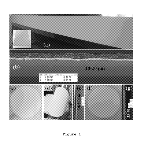
Figure 1 shows (a) Large area Ag films (Example 1) prepared
using tape caster and inset shows a rectangular piece of the
film on PET, (b) optical microscopic image of the free
standing dry film of 18-20 20pm thickness, (c-e) optical
microscopic images of free standing dry film of Example 2 on
PET (30-40 pm thickness) and (f-g) optical microscopic
images of free standing dry film of Example 5 on PET.
Figure 2 shows a schematic representation of die-attach
processes "Pressure Sintering (PS)" Vs. "Pressure Placement
and Pressure-less Sintering (PPPS)" process steps for die-
attach application of the sintering film of the present
invention.
Figure 3 shows a schematic representation of "Pressure
Placement and Pressure-less Sintering" process steps for
die-attach application of the sintering film of the present
invention and its typical process parameters and their
interdependencies.
CA 02944958 2016-10-05
WO 2015/155542
PCT/GB2015/051096
29
Figure 4 shows plots of die-shear of 3mmx3mm Ni/Au coated Si
dies attached on Ni/Ag coated DBC using the film of Example
2 as a function of a) placement time and b) tool temperature
using "Pressure Placement and Pressure-less Sintering Die-
attach Process".
Figure 5 shows SEM images of the cross-section area of
3mmx3mm Ni/Au coated Si dies attached on Ni/Ag coated DBC
using the film of Example 2 at placement time is using
"Pressure Placement and Pressure-less Sintering Die-attach
Process".
Figure 6 shows transferred Ag film on Ni/Au coated Si wafer
and remaining film on PET after transfer.
Figure 7 shows images of diced (3mmx3mm) samples from
thermo-compression bonded (a) Ni/Au coated 4" Si wafer pairs
and (b) Ni/Au coated 4" Si wafer with Ni/Au coated 4" CuW
wafer using 18-20 pm film of Example 2 prepared by
commercially available dicing machine. No chipping is
observed.
Figure 8 shows a C-SAM image of thermo-compression bonded
Ni/Au coated 4" Si wafer pairs using 18-20 pm film of
Example 1.
Figure 9 shows SEM images of the cross-section area of diced
samples revealing BLT and microstructures. These samples
were prepared from thermo-compression bonded Ni/Au coated Si
wafer pairs using 18-20 pm film of Example 1 at different
applied pressures: 0.5 (top left), 1 (top centre), 2 (top
right), 5 (bottom left)and 10 MPa (bottom centre).
CA 02944958 2016-105
WO 2015/155542
PCT/GB2015/051096
Figure 10 shows C-SAM images of thermo-compression bonded
Ni/Au coated 4" Si wafer pairs using 18-20 pm film of
Example 1 without post heating step (step 4).
5
Figure 11 shows representative CSAM image of thermo-
compression bonded Ni/Au coated 4" Si wafer with Ni/Au
coated 4" CuW wafer using 18-20 pm film of Example 1.
10 Figure 12 shows an SEM image of the cross-sectional area of
the ion-polished dies prepared from thermo-compression
bonded Ni/Au coated 4" Si wafers using 30-40 pm film of
Example 2.
15 Figure 13 shows a C-SAM image of thermo-compression bonded
Ni/Au coated 4" Si wafer with Ni/Au coated 4" CuW wafer
using film of Example 2. The C-SAM image confirms good
bonding and there is no delamination or void in the bonded
wafers.
Figure 14 shows an SEM image of the cross-sectional area of
the ion-polished dies prepared from thermo-compression
bonded 4" Si wafer with Ni/Au coated 4" CuW wafer using 30-
40 pm film of Example 2.
Figure 15 shows a plot of die-shear of 3mmx3mm sized dies
prepared from thermo-compression bonded Ni/Au coated 4" Si
wafers pairs and Ni/Au coated 4" Si wafer with Ni/Au coated
4" CuW using film of Example 1 and film of Example 2.
CA 02944958 2016-105
WO 2015/155542 PCT/GB2015/051096
31
The invention will now be described with reference to the
following non-limiting Examples.
Example 1
0 to 8% resin or polymer, 0 to 2% film forming agent and 5
to 30 % solvent mixture were mixed to get a homogeneous
solution. To this mixture, 0 to 2% wetting agents, 0 to 2 %
organic peroxides were added, followed by the addition of 65
to 85% of the aforementioned silver nanopowder (i.e. having
a mean longest dimension of from 5 to 75 nm) and was mixed
using an orbital mixer at 1000 rpm. After mixing, the
mixture was milled in a three roll mill for few minutes to
obtain a homogenous paste.
Example 2
0 to 2% film forming agent, 0 to 5 % silver metallo organic
compound (Ag MOC), 5 to 30 % solvent mixture were mixed in a
jar. To this mixture, 0 to 2% wetting agents, 0 to 2 %
organic peroxides were added, followed by the addition of 65
to 85% of the aforementioned silver nanopowder (i.e. having
a mean longest dimension of from 5 to 75 nm). This mixture
was mixed using an orbital mixer at 1000 rpm. After mixing,
the mixture was milled in a three roll mill for a few
minutes to obtain a homogenous paste.
Example 3
0 to 2% film forming agent, 0 to 8% resin or polymer, 0 to 5
% silver metallo organic compounds (Ag MOC) and 5 to 30 %
solvent mixture were mixed in a jar. To this mixture, 0 to
2% wetting agents, 0 to 2 % organic peroxides were added,
CA 02944958 2016-105
WO 2015/155542
PCT/GB2015/051096
32
followed by the addition of 65- 85% of the aforementioned
silver nanopowder(i.e. having a mean longest dimension of
from 5 to 75 nm). This mixture was mixed using an orbital
mixer at 1000 rpm. After mixing, the mixture was milled in a
three roll mill for a few minutes to obtain a homogenous
paste.
Example 4
0 to 2% film forming agent, 0 to 8% resin or polymer, 0 to 7
% silver metallo organic compounds (Ag MOC) and 5 to 30 %
solvent mixture were mixed in a jar. To this mixture, 0 to
2% wetting agents, 0 to 2 % organic peroxides were added,
followed by the addition of 65 to 95% of silver micron
particles (i.e. having a mean longest dimension of from 100
nm to 50 pm). This mixture was mixed using an orbital mixer
at 1000 rpm. After mixing, the mixture was milled in a three
roll mill for a few minutes.
Example 5
0 to 2% film forming agent, 0 to 8% resin or polymer, 0 to 7
% silver metallo organic compounds (Ag MOC) and 5 to 30 %
solvent mixture were mixed in a jar. To this mixture, 0 to
2% wetting agents, 0 to 2 % organic peroxides were added,
followed by the addition of 65- 95% of a mixture of silver
nano (i.e. having a mean longest dimension of from 5 to 75
nm)and micron particles(i.e. having a mean longest dimension
of from 100 nm to 50 pm). This mixture was mixed using an
orbital mixer at 1000 rpm. After mixing, the mixture was
milled in a three roll mill for a few minutes.
CA 02944958 2016-10-05
WO 2015/155542 PCT/GB2015/051096
33
Thermal conductivity of the sintered silver samples of
Examples 1-5 are found to be in the range of 100 - 250 W.m-
1.K-1. Thermal conductivity of the sintered silver samples
are prepared by heating the paste in Examples 1-5 at 250 C
for 60 min with no applied pressure and are measured using a
Netzsch LFA 447 Nanoflash. Thermal conductivity k (W.m-1.K-1)
was calculated using the following formula: K=a p cp, where,
a is thermal diffusivity (m2.s-1), p is the density of the
material (Kg.m-3) and cp is the specific heat capacity (J.kg-
1.K1).
Film preparation process:
Films were prepared by printing on silicon coated polyester
sheet either using a commercially available tape caster in
roll to roll fashion, using a micro gauge controlled doctors
blade assembly supplied with the tape caster or by manual
stencil printing using a doctor blade.
Commercially available tape caster:
The paste of Example 1 was printed on a silicon coated
polyester sheet using a commercially available tape caster
and was dried at 130 C on its heated surface in roll to
roll fashion. For complete drying, the film takes 10 to 15
minutes. The thickness of the film was controlled using the
gap setting of the doctor blade assembly supplied with the
tape caster. Film thicknesses of 18-20pm and 33-35pm were
prepared by changing the gap setting of the micro gauge
controlled doctor blade assembly. Fig. 1 (a) shows the large
area film prepared using tape caster and inset shows a
rectangular piece of the film on PET. Fig 1 (b) shows the
CA 02944958 2016-10-05 2015/155542
PCT/GB2015/051096
34
optical microscopic image of the free standing dry film of
18-20 20pm thickness. Films having thickness > 5pm can also
be easily obtained by simply changing the gap setting of the
doctor blade assembly.
Manual stencil printing:
The paste of Example 2 was manually stencil printed using a
doctor blade on silicon coated polyester. These as prepared
films were dried at 60-90 C in an oven for 30-90 minutes.
The thickness of such manually printed films of Example 2 is
found to be 20-60 pm. Optical microscopic images of free
standing dry film of Example 2 and Example 5 on PET (30-40
pm thickness) are shown in Fig. 1 (c-e) and Fig. 1 (f-g)
respectively. Alternatively, films also can be printed on
silicon coated polyester sheet using a commercially
available tape caster in roll to roll fashion and thickness
of the film can be controlled using the gap setting of the
micro gauge controlled doctor blade assembly supplied with
the tape caster.
Application of Ag films for die-attachment:
The sintering films of the present invention can be used for
the joining of electronic components using variety of silver
sintering based existing die-attached processes (Pressure
Sintering (PS) Process) including those as described in
patent application US 13/287820, the disclosure of which is
hereby incorporated by reference. In addition, the sintering
films of the present invention can be used in a die attach
"Pressure Placement and Pressure-less Sintering (PPPS)
process". Fig. 2 shows the schematic representation of the
general process steps of "Pressure Sintering (PS)" Vs.
CA 02944958 2016-105
WO 2015/155542
PCT/GB2015/051096
"Pressure Placement and Pressure-less Sintering (PPPS)"
process steps using the sintering films of the present
invention. There are several additional advantages for this
new PPPS process as compared to PS process viz., shorter
5 time required for die-placement (high UPH), low-pressure
requirement for placement (highly advantageous for
processing thin wafers), compatibility with commercial die-
bonder and sintering in external heating equipment (batch
process to improve UPH). Additionally, these sinterable Ag
10 films can also be used for PS process that require
significantly higher pressure (>5 MPa) during sintering
based die-attached processes.
Pressure Placement and Pressure-less Sintering (PPPS)
15 process:
The sintering films of the present invention can be used for
the joining of electronic components using a new silver
sintering low-temperature and low-pressure die-attach
20 process "Pressure Placement and Pressure-less Sintering
(PPPS) process". Fig. 3 shows the schematic representation
of "Pressure Placement and Pressure-less Sintering process"
steps for die-attach application of nano-Ag film, its
typical process parameters and their interdependence.
25 Joining of electronic components using this Pressure
Placement and Pressure-less Sintering process using this
sinterable Ag film is very versatile and the exact
combination of time, temperature and pressure can be
optimized based on the nature of application and thermo-
30 mechanical, electrical and thermal performance requirements.
PPPS die-attach process steps:
CA 02944958 2016-105
WO 2015/155542
PCT/GB2015/051096
36
The overall bonding process may typically include, for
example: 1) Film transfer, 2) Pressure Assisted Die
Placement and 3) Pressureless Sintering, unless stated
otherwise separately elsewhere.
(1) Film Transfer: Sinterable Ag film transfer on the die by
stamping process using optimized combination of time,
pressure and temperature of tool and plate. Typical process
parameters are:
Tool Temperature = Room Temperature to 400 C
.
Plate Temperature = Room Temperature to 400 C
.
Pressure = 0.1 to 5 MPa
.
Time = 0.1 to 60 s
.
(2) Pressure Assisted Die Placement: Placement of sinterable
Ag containing die on DBC (direct bonded copper) substrate
using optimized combination of time, pressure and
temperature of tool and plate. Typical process parameters
are:
Tool Temperature = Room Temperature to 400 C
.
Plate Temperature = Room Temperature to 400 C
.
Pressure = 0.1 to 40 MPa
.
Time = 0.1 to 60 min
.
Additional Heating Time : May include additional 0-60
min immediately after placement (without applying any
external pressure)
(c) Pressureless Sintering: Pressureless sintering is
carried out in an external oven or hot plate. Process
parameters are summarized below:
Sintering Temperature = 150-400 C
.
Sintering Time = 0 to 120 min
.
CA 02944958 2016-105
WO 2015/155542
PCT/GB2015/051096
37
Pressure Assisted Sintering (PS) process:
The sintering films described herein can be used for the
joining of electronic components using pressure assisted
sintering die-attach process. Joining of electronic
components using this pressure assisted sintering process
using this sinterable Ag film is very versatile and the
exact combination of time, temperature and pressure can be
optimized based on the nature of application and thermo-
mechanical, electrical and thermal performance requirement.
PS die-attach process steps:
The overall bonding process may typically include, for
example: 1) Film transfer, 2) Pressure Assisted Die
Placement and Sintering, unless stated otherwise separately
elsewhere.
(1) Film Transfer: Sinterable Ag film transfer on the die by
stamping process using optimized combination of time,
pressure and temperature of tool and plate. Typical process
parameters are:
Tool Temperature = Room Temperature to 400 C
.
Plate Temperature = Room Temperature to 400 C
.
Pressure = 0.1 to 5 MPa
.
Time = 0.1 to 60 s
.
(2) Pressure Assisted Die Placement and Sintering: Placement
of sinterable Ag containing die on DBC substrate using
optimized combination of time, pressure and temperature of
tool and plate. Typical process parameters are:
CA 02944958 2016-105
WO 2015/155542 PCT/GB2015/051096
38
Tool Temperature = Room Temperature to 400 C
.
Plate Temperature = Room Temperature to 400 C
.
Pressure = 0.1 to 40 MPa
.
Time = 0.1s to 60 minutes
.
Additional Heating Time : May include additional 0-60
min immediately after placement (without applying any
external pressure)
General characterization processes of bonded dies:
The bonded dies were characterized with die-shear, thermal
shock and cycling, bond-layer thickness measurements and
microstructure analysis, using SEM after ion-polishing.
Die-attach Application 1 (PPPS):
The application of the sintering film formed of Example 2
has been demonstrated for the joining of electronic
components using a pressure sintering process (Process
schematic is shown in Fig. 3). An example of such
application has been demonstrated attaching Ni/Au coated 3mm
x 3mm Si dies on Au or Ag coated DBC substrates using
sinterable Ag film using a laboratory manual die-bonder.
Fig. 4 shows die-shear results of 3mmx3mm Ni/Au coated Si
dies attached on Ni/Ag coated DBC using the sintering film
formed of Example 22 as a function of a) placement time and
b) tool temperature using "Pressure Placement and Pressure-
less Sintering Die-attach Process". Following process
parameters are used for die-attach:
(1) Film Transfer:
Tool Temperature = 100-200 C
.
Plate Temperature = Room Temperature
.
CA 02944958 2016-10-05
WO 2015/155542 PCT/GB2015/051096
39
Pressure = 1.5 MPa
.
Time = is
.
(2) Pressure Assisted Die Placement:
Tool Temperature = 100-200 C
.
Plate Temperature = 200 C
.
Pressure = 2
.
Time = 0.25 to 1.5 s
.
Additional Heating Time : None
(3) Pressureless Sintering:
Sintering Temperature = 225 C
.
Sintering Time = 60 min
.
Fig. 5 shows the SEM images of the cross-sectional area of
the ion-polished dies prepared from 3mmx3mm Ni/Au coated Si
dies attached on Ni/Ag coated DBC using sintering film
formed of Example 2 with 1 s placement time. The SEM of the
bonding layer shows the necking of the sintered silver
particles with a good packing fraction.
Die-attach Application 2 (PS):
The application of the sintering film formed of Example 5
has been demonstrated for the joining of electronic
components using a pressure assisted sintering process. An
example of such application has been demonstrated attaching
Ni/Au coated 3mm x 3mm Si dies on Au or Ag coated DBC or Ag
coated Cu lead frames substrates the sintering film formed
of Example 5 using a laboratory manual die-bonder by
applying sintering pressure 5-20 MPa at 250 C for 30-90s
sintering time. The die-shear results show strong bonding (>
CA 02944958 2016-105
WO 2015/155542 PCT/GB2015/051096
40 MPa) and the SEM of the bonding layer shows the necking
of the sintered silver particles with a good packing
fraction.
5 Application of Ag films for wafer bonding:
Thermo-compression bonding applications of a pair of Ni/Au
coated 4" Si wafers (Si-Sintered Ag-Si) and Ni/Au coated 4"
Si wafer with Ni/Au coated 4" CuW wafer (Si-Sintered Ag-CuW)
10 are demonstrated using a film formed of Example 1 and a film
formed of Example 2 at 250 C using 1 MPa pressure using a
laboratory press. For all of the demonstration of the wafer
bonding (application 1-4) using these films, the following
bonding processes are followed unless stated otherwise
15 elsewhere.
Wafer bonding process steps:
The overall bonding process may typically include, for
20 example: 1) Film transfer, 2) Wafer stack formation, 3)
Wafer bonding and 4) Post heating, unless stated otherwise
separately elsewhere.
1) Film transfer:
25 The Ag film is transferred from PET surface to either Ni/Au
coated Si or Ni/Au coated CuW at 80-150 C and 1 MPa pressure
for 5 min. The remaining Ag film and PET were removed and Ag
transferred Ni/Au coated Si or Ni/Au coated CuW wafers were
used for stack formation. Fig. 6 shows the images of
30 transferred Ag film on Ni/Au coated Si wafer and remaining
film on PET after transfer.
2) Wafer stack formation:
CA 02944958 2016-105
WO 2015/155542
PCT/GB2015/051096
41
Stack is prepared by placing a Ni/Au coated Si wafer on Ag
film transferred Ni/Au coated Si or Ni/Au coated CuW by step
1. The stack is then heated at 100-150 C and 1 MPa pressure
for 5-15 min.
3) Wafer bonding
Wafers stack processed by step 2 is used for bonding at
250 C and 1 MPa pressure for 15 min.
4) Post heating
Wafers stack processed at 250 by step 3 are used for post
heating at 250 C without any applied pressure for 45 min.
After these processes, bonded wafer is cooled to room
temperature and used for further characterization.
General characterization processes of bonded wafers:
All of the bonded wafers were inspected for delamination and
voids using C-SAM. These bonded wafers were then diced to
obtain different die sizes, like, 3mmx3mm & l0mmx10mm for
various characterizations, such as die-shear, thermal shock
and cycling, bond-layer thickness measurements and
microstructure analysis, using SEM after ion-polishing. For
example, Fig. 7 shows the images of diced (3mmx3mm) samples
using commercially available dicing machine prepared from
thermo-compression bonded (a) Ni/Au coated 4" Si wafer pairs
and (b) Ni/Au coated 4" Si wafer with Ni/Au coated 4" CuW
wafer, using 18-20 pm film of Example 1. No de-bonding and
chipping are observed for all of these bonded wafers,
indicating good bonding.
Wafer Bonding Application 1 (Si-AF1-Si)
Bonding at different applied pressure:
CA 02944958 2016-105
WO 2015/155542
PCT/GB2015/051096
42
Thermo-compression bonding of a pair of Ni/Au coated 4" Si
wafers are demonstrated using 18-20 pm film of Example 1 at
250 C using 0.5, 1, 2 and 5 MPa pressure using a laboratory
press. For 10 MPa pressure a pair of Ni/Au coated 2" Si
wafers were used. All of the bonded wafers were inspected
for delamination and voids using C-SAM and confirmed there
is no-delamination and voids. Fig. 8 shows the C-SAM image
of thermo-compression bonded Ni/Au coated 4" Si wafer pairs
using 18-20 pm film of Example 1. The C-SAM image confirms
good bonding and there is no delamination and voids in the
bonded wafers. These bonded wafers were then diced to
different die sizes, like, 3mmx3mm, l0mmx10mm and used for
determining die-shear, bond-layer thickness measurement and
microstructure analysis using SEM after ion-polishing. To
investigate the effect of the pressure on the microstructure
and bond line thickness (BLT) of the sintered silver layers,
these wafers were diced and investigated using SEM. Fig. 9
shows the SEM images of the cross-sectional area of the ion-
polished dies prepared from thermo-compression bonded pairs
Ni/Au coated Si wafers using 18-20 pm film of Example 1 at
different applied pressures: a) 0.5, b) 1, c) 2, d) 5 and e)
10 MPa. The SEM of the bonding layer shows the necking of
the sintered silver particles with a good packing fraction.
The BUT is found highly pressure dependent at the low
pressure region (0.5 to 2 MPa), after which the effect of
pressure on BUT becomes less prominent. In contrast, the
microstructure of these sintered silver are highly pressure
dependent throughout the experimentally applied pressure
range as evident from the crystallite size, interlinking
neighbors and density. As can be seen, at pressures of 5 and
10 MPa, it produces a highly dense and interlinked
structure. The die-shear of the bonded dies show bulk or
CA 02944958 2016-105
WO 2015/155542
PCT/GB2015/051096
43
interfacial failure and thus it can be concluded that the
sintered silver bonding materials is very strong as compared
to the bonded silicon wafer materials.
Bonding without post heating:
To confirm the necessity of the post heating step, we have
bonded two pairs of Ni/Au coated 4" Si wafers using the 18-
20 pm film formed of Example 1 at 250 C using 1 MPa
pressure using a laboratory press, without performing post
heating step (step 4). As it can be clearly seen in Fig. 10,
there are several delaminating areas present in these
wafers.
Wafer Bonding Application 2 (Si-AF1-CuW):
Thermo-compression bonding of Ni/Au coated 4" Si wafer with
Ni/Au coated 4" CuW wafer are demonstrated using 18-20 pm
film formed of Example 1 at 250 C using 1 MPa pressure
using a laboratory press. Fig. 11 shows the C-SAM image of
thermo-compression bonded Ni/Au coated 4" Si wafer with
Ni/Au coated 4" CuW wafer using 18-20 pm film of Example 1.
The C-SAM image confirms good bonding and there is no
delamination and voids in the bonded wafers. These bonded
wafers were then diced to different die sizes like, 3mmx3mm
& l0mmx10mm and used for determining die-shear, bond-layer
thickness measurement and microstructure analysis, using SEM
after ion-polishing. To investigate the effect of film
thickness on the bond line thickness (BLT) of the sintered
silver layers, we have chosen 18-20 and 32-35 pm films
formed of Example 1 to bond 4" Si wafer with Ni/Au coated
4" CuW wafer at 250 C using 1 MPa pressure using a
CA 02944958 2016-105
WO 2015/155542
PCT/GB2015/051096
44
laboratory press. The SEM of the bonding layer shows the
necking of the sintered silver particles with a good packing
fraction. The BUT is found to be decreased with decreasing
the film thickness. The die-shear of the bonded dies shows
bulk or interfacial failure and thus it can be concluded
that the sintered silver bonding materials is very strong as
compared to the bonded silicon wafer materials.
Wafer Bonding Application 3 (Si-AF2-Si):
Thermo-compression bonding of a pair of Ni/Au coated 4" Si
wafers are demonstrated using 30-40 pm film of Example 2 at
250 C using 1 MPa pressure using a laboratory press. All of
the bonded wafers were inspected for delamination and voids
using C-SAM and confirmed there is no-delamination and
voids. C-SAM images of thermo-compression bonded Ni/Au
coated 4" Si wafer pairs using 30-40 pm film of Example 2
confirms good bonding and there is no delamination and voids
in the bonded wafers. These bonded wafers were then diced to
different die sizes, like, 3mmx3mm, l0mmx10mm and utilized
for die-shear, and bond-layer thickness measurements and
microstructure analysis, using SEM after ion-polishing. Fig.
12 shows the SEM images of the cross-sectional area of the
ion-polished dies prepared from thermo-compression bonded
pairs Ni/Au coated 4" Si wafers using 30-40 pm film of
Example 2 at 1 MPa applied pressure. The SEM of the bonding
layer shows the necking of the sintered silver particles
with a good packing fraction. The die-shear of the bonded
dies show bulk or interfacial failure and thus it can be
concluded that the sintered silver bonding materials is very
strong as compared to the bonded silicon wafer materials.
Wafer Bonding Application 4 (Si-AF2-CuW):
CA 02944958 2016-105
WO 2015/155542
PCT/GB2015/051096
Thermo-compression bonding of Ni/Au coated 4" Si wafer with
Ni/Au coated 4" CuW wafer are demonstrated using 30-40 pm
film of Example 2 at 250 C using 1 MPa pressure using a
5 laboratory press. Fig. 13 shows the C-SAM image of thermo-
compression bonded Ni/Au coated 4" Si wafer with Ni/Au
coated 4" CuW wafer with 30-40 pm film of Example 2. The C-
SAM image confirms good bonding and there is no delamination
and void in the bonded wafers. These bonded wafers were then
10 diced to different die sizes like, 3mmx3mm & l0mmx10mm and
utilized for die-shear and bond-layer thickness measurements
and microstructure analysis using SEM after ion-polishing.
Fig. 14 shows the SEM images of the cross-sectional area of
the ion-polished dies prepared from thermo-compression
15 bonded 4" Si wafer with Ni/Au coated 4" CuW wafer using 30-
40 pm film of Example 2 at 250 C using 1 MPa pressure. The
SEM of the bonding layer shows the necking of the sintered
silver particles with a good packing fraction. The die-
shear, of the bonded dies, shows bulk or interfacial failure
20 and thus, it can be concluded that the sintered silver
bonding materials is very strong as compared to the bonded
silicon wafer materials.
Mechanical and thermo-mechanical characterization of bonded
25 wafers
Die-shear results:
To investigate the mechanical bond strength of bonding
30 sintered Ag layer, the thermo-compression bonded wafers were
diced into 3mmx3mm sized die and die-shear test performed.
The die-shear of the bonded dies show bulk or interfacial
CA 02944958 2016-10-05
WO 2015/155542
PCT/GB2015/051096
46
failure and thus it can be concluded that the sintered
silver bonding materials is very strong as compare to the
bonded silicon wafer materials. Fig. 15 shows comparison of
the die-shear values of 3mmx3mm sized dies prepared from
thermo-compression bonded pair of Ni/Au coated 4" Si wafers
and Ni/Au coated 4" Si wafer with Ni/Au coated 4" CuW wafer
using a film formed of Example 1 and a film formed of
Example 2 at 250 C using 1 MPa pressure.
Thermal shock results:
To investigate the effect of thermal stress on the bonded
wafer and dies using sintered nano-sliver films, the thermo-
compression bonded 4" Si wafer with Ni/Au coated 4" CuW
wafer using a film formed of Example 1 and a film formed of
Example 2 at 250 C and 1 MPa pressure and 10mm x 10mm dies
were subjected to thermal shock experiments following the
JESD22-A104-B Test Condition B, Soak Mode 2 (- 55 to +125
C, 5 mins dwell time, 1000 cycles). The C-SAM images of
both the bonded wafers and dies post 1000 cycles do not
reveal any delamination, voids and cracks in the bonded
wafers.
Thermal cycling results:
To investigate the effect of thermal stress on the bonded
dies using sintered nano-sliver films, 10mm x 10mm diced
samples from the thermo-compression bonded 4" Si wafer with
Ni/Au coated 4" CuW wafer using film formed of Example 1 and
film formed of Example 2 at 250 C and 1 MPa pressure were
subjected to thermal cycling experiments following the IPC
9701-A Standard TC3 / NTC-C Profile (-40 to +125 C, 15 mins
CA 02944958 2016-10-05 2015/155542 PCT/GB2015/051096
47
dwell time, 1000 cycles). The C-SAM images of these dies
post 1000 cycles do not reveal any delamination, voids and
cracks in the bonded wafers.
Other applications of the sintering powders, sintering films
and sintering pastes of the present invention are as
follows:
1. Wafer-to-wafer bonding layers for Vertical LED Designs,
Thin Film Flip Chip Designs and Red LED Designs, based on
both printable pastes and films. There is a significant
need for wafer-to-wafer bonding at low temperatures (under
250 C and also under 200 C) where the bonding layer
exhibits very high temperature properties post bonding. In
the case of LED wafer bonding, this can be accomplished for
example, in the context of either thin film flip chip or
vertical thin film or truncated inverted pyramid LEDs, where
CTE mismatch and therefore strain and defect generation can
be minimized, while allowing for high temperature post
processing with a variety of advanced materials for
enhancing light output and electrical efficiency of the
device. Further, the high temperature and high thermal and
electrical conductivities of the bonding layer allow for
superior thermal transfer, high temperature operation of the
device and superior current spreading, among other
advantages. Such wafer bonding can be accomplished by
lamination of films of the said material on the backside of
the wafers, followed by temperature and pressure processing
in a standard wafer bonder or a press. Another means of
doing the processing includes printing a conformal layer of
paste on the wafer backside, followed by drying and bonding
in a standard wafer bonder or press, under temperature and
pressure conditions. Other applications for such wafer
CA 02944958 2016-105
WO 2015/155542
PCT/GB2015/051096
48
bonding include power semiconductor wafers, Through Silicon
Via (TSV) applications, stacked die applications, MEMS,
concentrated photovoltaic and other applications. Low
temperature sintering enables assembly of high CTE mismatch
stacks as well as temperature sensitive material stacks,
thermoelectric materials and piezoelectric materials.
2. Attachment of semiconductor die (either flip chip or wire
bonded), onto a variety of substrates such as DBC (Direct
Bond Copper), DPC (Direct Plate Copper), MCPCB (Metal Core
PCBs), FR4, Copper lead-frames, Flexible PCBs and
substrates, Copper and Aluminum Heat-Sinks, Fixtures, etc.).
Applications include LED die (light emitting diodes for
example of the lateral, vertical thin film or flip chip
varieties) made from various compound semiconductor
materials, power die made from silicon, concentrated
photovoltaic compound semiconductor cells (e.g. multi-
junction cells) silicon carbide and gallium nitride used in
power modules, and discrete devices, MEMS (micro-
electromechanical sensor) devices of all types,
semiconductor and stacked die and other applications such as
thermoelectric materials and piezoelectric materials.
(a) The attachment of such semiconductor or other die
elements can be accomplished by printing on to the
substrates, followed by die placement via a die bonder or a
pick and place machine, and sintering in either a reflow
oven belt or box oven. Attachment of such semiconductor and
die elements can also be accomplished via dispensing the
paste, followed by die placement and sintering as outlined
above, or doing film transfer and lamination on the die
backside of the film made from the said material, followed
by die placement and tacking onto the substrate, followed by
sintering. Flip chip die can be assembled by printing bumps
CA 02944958 2016-10-05 2015/155542
PCT/GB2015/051096
49
on the substrate, placing the die, followed by sintering.
Low temperature sintering enables assembly of high CTE
mismatch stacks as well as temperature sensitive material
stacks.
3. Attachment of semiconductor packages of various types
(for example bottom termination components such as LGAs,
QFNs, QFPs, etc.), onto a variety of substrates such as DBC
(Direct Bond Copper), DPC (Direct Plate Copper), MCPCB
(Metal Core PCBs), FR4, Flexible PCBs and substrates, Copper
and Aluminum Heat-Sinks, Fixtures, etc.). Applications
include LED packages of various types (for example, ceramic
sub-mount LEDs, SMD LEDs with lead-frame construction, etc,)
power modules, and discrete devices, MEMS (micro-
electromechanical sensor) packages of all types,
semiconductor and stacked die packages and other
applications.
(a) The attachment of such semiconductor or other
packages can be accomplished by printing on to the
substrates, followed by package placement via standard pick
and place machine with Z Height adjustment and / or pressure
capability, and sintering in either a reflow oven belt oven
or box oven. Low temperature sintering enables assembly of
high CTE mismatch stacks as well as temperature sensitive
material stacks.
4. Production of interconnect lines ('circuitry, pads, etc.)
separately and along with flip chip interconnects. For
example, applications for interconnect lines include LED
boards and luminaires, where the interconnect lines can be
applied by a variety of printing (e.g. stencil printing) or
dispensing or jetting techniques. In the case of LED
applications, such interconnects can serve as both
CA 02944958 2016-10-05 2015/155542
PCT/GB2015/051096
electrical and thermal conductors to carry the electrons to
and from the device, and the heat away from the device.
Further, such interconnect lines can be directly applied in
the same step with interconnects for attaching flip chip or
5 wire bonded devices. Another example of such interconnects
is solar cells (either silicon based or thin film based),
where the interconnects in a grid pattern could be used to
collect electrons generated, and also connect one cell to
another.
5. Reflective layer printing for LED and optical
applications. The said material can be used to print
reflective layers on to substrates such as DBC (Direct Bond
Copper), DPC (Direct Plate Copper), MCPCB (Metal Core PCBs),
FR4, Flexible PCBs and substrates, Copper and Aluminum Heat-
Sinks, Fixtures, etc.), in order to provide light output
enhancement and therefore luminous efficacy enhancement of
LED and other optical systems. Such reflective layers can
be formed via stencil or screen printing, jetting or
dispensing or film lamination of the said material.
6. Hermetic and near hermetic sealing for packages,
perimeter seals, etc. for LED, MEMS, OLED and PV
applications and general semiconductor packaging. There is
a significant need for hermetic sealing of LED, OLED, MEMS
and thin film PV packages, to protect the devices from
moisture ingress. The said material can exhibit hermetic or
near hermetic sealing behavior with proper application and
sintering. The said material can be applied in various
stages of the manufacturing processes for the above devices:
Either at the wafer level with wafer bonding, or in the
packaging process via film lamination and bonding, or paste
jetting/dispensing followed by lid or glass or laminate
CA 02944958 2016-10-05
WO 2015/155542
PCT/GB2015/051096
51
cover attach and sintering. Low temperature sintering
enables assembly of high CTE mismatch stacks as well as
temperature sensitive material stacks.
7. ACE Replacements. Arrays of bumps of the said material
can be delivered to the substrate via stencil printing, bump
transfer, or high speed jet dispensing. Such arrays can be
used to serve as electrical contacts to assemble devices
without explicit high degrees of alignment