Note: Descriptions are shown in the official language in which they were submitted.
CA 02945093 2016-10-06
WO 2015/156854 PCT/US2015/010274
Multi-Module DC-to-DC Power Transformation System
FIELD
This innovation pertains to conversion of electric power from one de voltage
to another
de voltage without the use of magnetically-based transformers.
BACKGROUND
Technologies used in conversion between alternating current (ac) and direct
current (dc)
have advanced rapidly over the past decades, as has the use of de as a means
of transporting
large amounts of power. De transports power more efficiently than ac and
unlike ac, is able to do
so at a controlled level, e.g. at a level corresponding to the maximum thermal
capability of the
conductors used.
The number of high voltage dc transmission projects has grown in distance,
voltage level
and power rating. Furthermore the need for dc-to-dc transformation has been
limited since,
irrespective of the dc transmission voltage, ac transformers are included in
both sending and
receiving terminals so that conversion to a voltage convenient to the local
system is quite straight
forward. However ongoing evolution of the world's electric supply system gives
rise to at least
four general applications where direct dc-to-dc transformation can have an
important role.
1. Both in Europe and North America, system planners foresee the need for an
extensive,
very high voltage dc network to serve as an overlay to the existing ac
transmission system.
However in addition to the connection of such a grid to key points in that ac
system, an
economic dc-to-dc transformer will allow both interconnection of that grid to
a number of
major existing dc transmission lines and transformation of different dc
voltages among dc
lines comprising a dc grid, thereby providing major additional economic
benefits to
consumers of electricity.
2. In context of a de grid the ac-to-dc converters that connect ac systems to
the dc grid will
have limited control of power through the various dc transmission lines
comprising the
grid. De-to-de transformers placed strategically in the dc grid will provide a
desired de
power flow through the transmission lines of the de grid where it is not
possible to
accomplish with the ac-to-dc converters
CA 02945093 2016-10-06
WO 2015/156854 PCT/US2015/010274
2
3. The electrical architecture of wind farms is relatively complex and, in
some systems,
makes use of ac-to-dc conversion at the wind turbine site to accommodate the
asynchronous nature of the ac voltage generated by variable speed blades.
Rather than
reconvert that de to synchronous ac, as is now the practice, direct
transformation of that de
energy to a higher dc level for aggregation within a wind farm, and to a yet
higher de
voltage for transmission to a load center, could affect major cost reductions
in the
aggregation of power at a central point on the wind farm as well as
transmission of the
collected power to a convenient point on the ac receiving system.
4. Household, commercial, and industrial loads are increasingly either
dependent on de or, in
some cases, could operate more efficiently if converted to dc. Charging load
for electric
automobiles, projected to grow very rapidly as a percentage of total
electrical load, is a
prime example. This realization has steadily increased the interest in dc
distribution
systems whereby de loads, rather than depending on either small scale plug-in
or internal
ac-to-dc converters, could be served directly from existing distributions
poles or cable
routes.
DESCRIPTION OF PRIOR ART
There is a wealth of technology, patent filings, and experience with dc-to-dc
conversion
at very low voltage (electronic) levels, e.g. within power supplies for
computers, telephones, and
other electronic devices. However this technology has been developed with
vastly different
needs and different constraints than those characterizing higher voltage power-
level applications
as addressed in the present disclosure. For example insulation requirements at
the millivolt level
are a secondary issue, while at high dc voltage it is paramount. Available
switching devices
differ as well, as do constraints on practical capacitor-to-capacitor and
capacitor-to-node
switching methods. At electronic levels heat generation is a greater limit to
losses than efficiency
whereas the reverse is true in high voltage power applications. Furthermore,
since inclusion of
reactors within circuit boards is impractical, transfer of charge from one
capacitor to another or
between two capacitors must be done directly, thus resulting in high losses.
Thus opportunities
for direct adaptation of electronic technology to high voltage dc applications
are limited.
Where conversion of between two higher de voltages is needed, as is the case
in some
industrial applications, de is first converted to a convenient ac level, often
at a high ac frequency
to reduce the cost of a transformer used to change to another ac voltage and
thence, through an
CA 02945093 2016-10-06
WO 2015/156854 PCT/US2015/010274
3
ac-to-dc then transformed by a conventional inductive transformer to a
different ac voltage, and
finally transformed from ac to the desired de secondary voltage. While
effective technically,
triple transformation schemes of this type are expensive and relatively
inefficient.
SUMMARY
The foregoing illustrates the need for an efficient and economical de-to-de
transformer
(DCT) (i.e., a transformation system at high power levels) capable of both
upward and
downward transformation of voltage and, where necessary, operating at the
highest existing dc
voltage levels at ratings in the thousands of megawatts. To match the
functionality of ac
transformers through which power transfer is proportional to phase angle
difference between
primary and secondary systems, a DCT should operate, without a power
controller, to the
difference in voltage between primary and secondary systems. The systems and
methods for
capacitive energy transformation described herein are capable of fulfilling
that requirement with
efficiencies comparable to existing ac-to-ac magnetic transformation.
Resonant switching, i.e. the connection between capacitors and a high voltage
node
through a reactor such that energy interchange is oscillatory and can be
interrupted at the first
current zero, is used in this disclosure. It will find application in various
situations analogous to
the function served by magnetically-based transformers in ac systems, e.g.
regulating power flow
between two or more dc systems or among multiple lines comprising a high
voltage dc grid as
well as transforming modest levels of power from a very high de voltage at
which dc-to-ac
conversion is uneconomic to a lower dc voltage level where conversion to ac is
less costly. It
will also find application in transformation of variable frequency sources
such as wind
generators to a higher dc voltage, resulting in more economic connection of
individual wind
generators to a common point and connection of their aggregation to a
convenient point on the
receiving ac grid, as well as conversion of ac to dc for distribution, as dc,
to homes, business and
industry. Other applications of the subject system will be apparent to those
skilled in the art and
are within the scope of this disclosure.
This disclosure features a multi-module de-to-de power transformation system
that is
constructed and arranged to transform power from a first high de voltage node
to a separate
second high dc voltage node. The system includes (a) a column comprising a
plurality of half-
bridge modules connected in series, each half-bridge module comprising a
series connected
CA 02945093 2016-10-06
WO 2015/156854 PCT/US2015/010274
4
capacitance capable of being either electrically inserted into the column or
electrically isolated
and electrically bypassed, wherein a first end of the column is electrically
connected to ground,
(b) two high voltage switches, each in series with a reactor; one high-voltage
switch adapted to
electrically connect a second end of the column to the first high voltage node
and the other
high-voltage switch adapted to electrically connect the second end of the
column to the second
high voltage node, and (c) a controller adapted to control the states of the
switches within the
column and the two high voltage switches so as to transform power by resonant
exchange of
energy between multiple capacitances within the column and the two nodes.
A half-cycle of resonant and sinusoidally varying current, initiated by the
connection of
multiple capacitances of the column to high voltage nodes and interrupted at
its first current-zero
point, may be used by the controller as a means to achieve exchange of energy
between those
multiple capacitances and the high voltage nodes. A ratio of input and output
voltage can be
established by causing the controller to affect switch positions which
electrically bypass selected
capacitances of the column between acceptance of charge from the first high
voltage de node and
delivery of charge to the second high voltage dc node.
Stable operation may be achieved by equalizing the charge on a group of
capacitances,
such charge equalization accomplished by using the controller to selectively
reassign by-pass
states among multiple capacitances during the connection to a lower voltage
node. Stable
operation may be achieved by using the controller to bypass different
capacitances from one
charge-discharge cycle to the next.
The system may have multiple columns connected in parallel between ground and
the
two high voltage nodes, with separate high-voltage switches in series with a
reactor between the
second end of each column and each of the two nodes, and wherein the
controller is adapted to
control the states of all of the switches. The controller may be further
adapted to establish input
and output current pulses to or from multiple columns that are additive. The
controller may be
further adapted to cause the generation of pulses from each of the columns and
that are equally
spaced in time from each other.
A half-cycle of resonant and sinusoidally varying current, initiated by the
connection of
multiple capacitances of the column to high voltage nodes and interrupted at
its first current-zero
point, may be used by the controller as a means to achieve exchange of energy
between those
CA 02945093 2016-10-06
WO 2015/156854 PCT/US2015/010274
multiple capacitances and the high voltage nodes. A ratio of input and output
voltage may be
established by causing the controller to affect switch positions which
electrically bypass selected
capacitances of each column between acceptance of charge from the first high
voltage dc node
and delivery of charge to the second high voltage de node.
Stable operation may be achieved by equalizing the charge on a group of
capacitances in
each column, such charge equalization accomplished by using the controller to
selectively
reassign by-pass state among multiple capacitances during the connection to a
lower voltage
node, Stable operation may be achieved by using the controller to bypass
different capacitances
in each column from one charge-discharge cycle to the next.
Also featured herein is a system for power transfer regulation from a first
node at one
high dc voltage to a second node at nominally the same high dc voltage. The
system includes a
plurality of capacitances and a controller that is adapted to use the
capacitances so as to
resonantly exchange energy between the capacitances and the two nodes.
A half-cycle of resonant and sinusoidally varying current, initiated by the
connection of
multiple capacitances of the column to high voltage nodes and interrupted at
its first current-zero
point, may be used by the controller as a means to achieve exchange of energy
between those
multiple capacitances and the high voltage nodes. A ratio of input and output
voltage can be
established by causing the controller to affect switch positions which
electrically bypass selected
capacitances between acceptance of charge from the first high voltage de node
and delivery of
charge to the second high voltage de node.
Stable operation may be achieved by equalizing the charge on a group of
capacitances,
such charge equalization accomplished by using the controller to selectively
reassign by-pass
state among multiple capacitances. Stable operation may be achieved by using
the controller to
bypass different capacitances from one charge-discharge cycle to the next.
The controller may be further adapted to establish input and output current
pulses to or
from multiple columns that are additive. The controller may be further adapted
to cause the
generation of pulses that are equally spaced in time from each other. A half-
cycle of resonant and
sinusoidally varying current, initiated by the connection of multiple
capacitances of the column
to high voltage nodes and interrupted at its first current-zero point, may be
used by the controller
as a means to achieve exchange of energy between those multiple capacitances
and the high
CA 02945093 2016-10-06
WO 2015/156854 PCT/US2015/010274
6
voltage nodes. A ratio of input and output voltage can be established by
causing the controller to
affect switch positions which electrically bypass selected capacitances
between acceptance of
charge from the first high voltage dc node and delivery of charge to the
second high voltage dc
node. Stable operation may be achieved by equalizing the charge on a group of
capacitances,
such charge equalization accomplished by using the controller to selectively
reassign by-pass
state among multiple capacitances during the connection to a voltage node.
Stable operation may
be achieved by using the controller to bypass different capacitances from one
charge-discharge
cycle to the next.
BRIEF DESCRIPTION OF THE DRAWINGS
Other objects, features and advantages will occur to those skilled in the art
from the
following description of the preferred embodiments of the innovations and the
accompanying
drawings.
Figure 1 shows a power level half-bridge module with internal switches
configured to
disconnect and bypass the internal capacitor.
Figure 2 shows a power level half-bridge module with internal switches
configured to
insert the internal capacitor into the circuit to which it is connected.
Figure 3 shows a multi-modular dc-to-dc power transformation system embodiment
configured for initial pre-operational charging of capacitors within half-
bridge modules.
Figure 4 shows a multi-modular dc-to-dc power transfoimation system embodiment
configured to receive charge from one high voltage de node.
Figure 5 shows a multi-modular dc-to-dc power transformation system configured
to
deliver charge to a second high voltage dc node.
Figure 6 shows the resonant nature of the low voltage input current pulse and
the output
current pulse in a multi-modular dc-to-dc power transformation system.
Figure 7 shows an example in which multiple multi-modular dc-to-dc
transformation
systems are used both to smooth input and output current levels and to
increase the power
capability of a compound dc-to-dc transformation system.
CA 02945093 2016-10-06
WO 2015/156854 PCT/US2015/010274
7
Figure 8 shows the nature of input and output current wave-form resulting from
an
example compound dc-to-dc transformation system comprised of three individual
dc-to-dc
transformers.
EMBODIMENTS
To simplify explanation of the embodiments cited herein, commonly used power
electronic switching devices such as thyristors, insulated gate bipolar
transistors (IGBTs) and
diodes, are all represented herein by a simple switch symbol, their function
being clear from the
context of the figures presented. Furthermore the more general identification
of "nodes" will, in
high voltage power applications correspond to "busses."
Embodiments cited herein are based solely on electrical charge transfers
between high
voltage dc busses and multiple capacitors. Transfers of that kind would result
in high losses
unless done resonantly, i.e. by placing an inductance in series with the
switch effecting the
transfer, thus causing a resonant sinusoidal wave of current which can be
interrupted at current
zero by power electronic switching devices, e.g. thyristors or solid state
bidirectional switches,
leaving the capacitor(s) involved with either an increase or decrease in
charge and a
corresponding higher or lower voltage. The principles of such resonant
transfers are well known
to those versed in the art.
Capacitor(s) 93 involved in one embodiment of the present system is embedded
in a half-
bridge module 90 as illustrated in figure 1. The term "half- bridge" as used
in this disclosure
refers either to (1) a composite capacitor and switch module as shown in
figure 1 which is
capable of either electrically inserting a capacitance into a series circuit
or isolating that
capacitance and bypassing it within the same series circuit and is commonly
identified with the
name "half-bridge," or (2) any other configuration of switches and
capacitances which
collectively function as the half-bridge described above. Note that the
capacitance 93 is
illustrated as a single capacitor but the capacitance could also be
accomplished with a series of
electrically coupled capacitors or other devices that exhibit capacitance.
Also shown in figure1 is a controller 110 which regulates the sequence and
timing of all
switches in the various embodiments described herein; this controller is
present in each example
but is not shown in every drawing. The controller can be part of a custom
circuit that includes the
half bridges or it can be a separate controller that is operably coupled to
the switches. Figure 1
CA 02945093 2016-10-06
WO 2015/156854 PCT/US2015/010274
8
also shows a commonly applied protective device 94 to protect elements within
the half-bridge in
the event of an electrical fault in the system within which it is applied.
Such modules 90 may
consist either of independently arrayed switches 91, 92 and capacitor 93 or
commercially
available and commonly applied half-bridge modules 90 consisting of the same
components 91,
92, 93. Commercially available modules are equipped with capacitors 93 of
relatively high
microfarad rating.
Capacitor 93 may be either inserted into circuit 20 by opening of switch 91
and closing
switch 92, or removed from circuit 20 and bypassed by opening switch 92 and
closing switch 91.
Changing from one state to another within such a module 90 can be achieved in
the order of
microseconds; orders of magnitude shorter than a reasonable period of resonant
charge exchange
between capacitors 93. Whereas figure 1 shows the capacitor 93 within the half-
bridge
disconnected from the series circuit of which it is a part by the closing of
switch 91 and opening
of switch 92, figure 2 shows the same capacitor 93 inserted into the series
circuit by opening of
switch 91 and closing of switch 92.
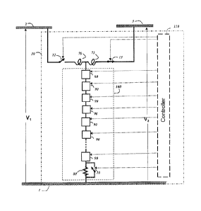
Figure 3 illustrates a basic embodiment of a multi-module dc-to-dc power
transformation
system 30 disclosed herein which uses a column 100 comprised of multiple half-
bridge modules
90 connected in series. Column 100 can be alternately connected either to a
first high voltage dc
node 2 through reactor 70 and switch 12 or a second high voltage dc node 3
through a second
reactor 71 and second switch 13. In practice, these switches 12 and 13 and
their counterparts in
subsequent drawings are complementary, i.e. when one switch is closed the
other will always be
open, thus always providing galvanic isolation between the two high voltage dc
nodes 2 and 3.
Reactors 70 or 71 may be made to vary in value when the de voltage transformer
ratio is made
adjustable.
The embodiment shown in figure 3 will operate either as a step-up or a step-
down
transformer of energy. In either case this embodiment operates with two
repetitive steps which
comprise an operating cycle. Consider first operation as a step-up DCT
Start-up
Assume there are a total of n half-bridge modules 90 within the column of
capacitive
modules 100, each containing a capacitor 93 which can, as illustrated in
figure 1, be
electrically inserted into that column 100 or bypassed and electrically
removed from that
CA 02945093 2016-10-06
WO 2015/156854 PCT/US2015/010274
9
column 100. Assume further, that the V2 > V1 so that the DCT illustrated in
figure 3 is
intended to convert energy at a nominal voltage V1 up to energy at a higher
nominal
voltage V2. During initial start-up energization, switch 12 is open and switch
13 is caused
to close as shown in figure 3, thus providing an initial charging path for the
column of
capacitive modules 100 from the second high voltage node 3 to ground 1. During
this
initial charging, switch 10 is opened, inserting resistor 80 into the initial
charging path,
thereby avoiding resonant overshoot and leaving each of the n capacitors 93
within the
column of modules 100 with a charge of V2/n. Switch 13 is then opened and
switch 10
permanently closed for normal operation. Ground is defined as being either an
actual
ground, or to a metallic return conductor, or to the same end of another DCT
connected to
a pole of opposite polarity in a dc system with no immediate ground.
Step 1:
Switch 13 being now open, m (where m is less than n) capacitors 93 within the
capacitive
modules 90 comprising the column 100 are bypassed, thus leaving the capacitive
column
100 with a reduced voltage of (n-m)/n x V2. Suppose, for example, that n and m
are
selected such that the ratio (n-m)/n is exactly equal to VI/V2. In that ease
the voltage on
either side of switch 12 will be the same and closing that switch 12 as
illustrated in figure
4 will cause no charge transfer from the first high voltage bus 2 to the
capacitive column
100. Suppose however that the voltage on the first high voltage node 2 is
caused to be
somewhat greater than (n-m)/n X V2. In that case closing of switch 12 in
figure 4 will
result in a resonant charge transfer from the first high voltage node 2 to n-m
of the
capacitors 93 within the capacitive column 100 while, as noted above, m of
those
capacitors 93, still bypassed remain charged to V2/n. If both the m bypassed
capacitors 93
and the n-m unbypassed capacitors, in series, were then simply connected
resonantly to
the second high voltage bus 3 as shown in figure 5, the voltage of the
capacitive column
100 would exceed V2 and result in energy being transferred to that bus. The
result
however would also leave n-m capacitors with higher post-discharge voltage
than the m
capacitors ¨ a difference that would grow with each repeating cycle. Thus
within this
embodiment, during the resonant half cycle of charging time during which n-m
capacitors
93 are receiving charge from the first high voltage node 2 as shown in figure
4, the actual
number of the bypassed capacitors remains equal to m. However, the
capacitor(s) that are
CA 02945093 2016-10-06
WO 2015/156854 PCT/US2015/010274
bypassed should be rotated among capacitors 93, in one or multiple cycles in a
sequence
and for time durations that assures that all capacitors, m and n-m have equal
charge and
voltage variations. This is a commonly used charge equalization process called
"sorting."
Step 2:
This step consists only of closing switch 13 to resonantly discharge the total
capacitive
column 100, now with all bypasses removed, to the second high voltage bus 3 as
is
shown in figure 5.
A modification of this embodiment, which will also overcome the cumulative
unbalance
in capacitor voltages cited above and remedied above by sorting procedures,
can be achieved by
continually rotating the assignment of bypassed capacitors between charge and
discharge cycles.
Thus a capacitor which is bypassed in one cycle may not be bypassed in the
next several cycles,
and a capacitor not bypassed in that cycle may be bypassed in the next, the
selection in each case
being made so as to stabilize charge distribution among all capacitors over a
large number of
cycles.
It will be apparent from the above that in this embodiment the amount of power
flowing
from the primary node 2 to the secondary node 3 will depend on the degree to
which the primary
voltage rises above V2 x (n-m)/n and, further, that if that voltage on the
primary bus 2 falls below
V2 x n-m)/n, the sequence set forth above will result in power flow from
second high voltage
node 3 to the first high voltage node 2.
It is equally apparent that flow direction and level will respond in the same
manner to
changes in the voltage level of the secondary node 3. These changes in power
flow are the
consequence of external voltage adjustments rather than a power control
signal. Thus flow
through this dc transformation system embodiment will be governed by the ratio
of terminal
voltages in relationship to the ratio of n and m, just as, with an ac
transformer, flow is dictated by
the phase angle difference of the systems on its two terminals. If this
embodiment is used to link
to independent de systems it will exchange power between those systems without
internal power
controls and in response to voltage adjustments on either system. Furthermore
if the embodiment
links two dc systems of identical voltage, variations in the selection of m,
the number of
bypassed capacitors 90, during the course of operation of those two systems
can be used allow
control of power flow in either direction between those two systems.
CA 02945093 2016-10-06
WO 2015/156854 PCT/US2015/010274
11
The number of capacitive modules 90 provided in the column 100 may exceed the
number used in the process described above in order to be inserted to replace
a capacitive
module 90 which fails in operation and is permanently bypassed pending
replacement.
Explanation of the foregoing embodiment was based on step-up operation of the
embodiment discussed. It will be apparent to those versed in the art that the
reverse sequence of
operation will transfer power from a higher to a lower voltage bus,
constituting step-down
operation.
The voltage ratio of the DCT can be changed by changing the number of bypassed
capacitors during Step 1 and adjusting the value of the reactor accordingly to
maintain the same
resonant frequency. Thus another embodiment of the invention, wherein the
number m of
bypassed capacitors is varied, can be used within a high voltage de grid to
regulate flow on one
or more particular lines.
Resonant switching within the foregoing method and system will result in both
input and
output pulse wave forms of the nature shown in figure 6; a waveform that would
be very difficult
to convert to a useful, constant de current. However a second (compound)
embodiment of this
invention consists of two or more DCTs in parallel (three in the example
illustration of figure 7)
wherein each is caused to generate pulses equally spaced in time from each
other; thus producing
a series of additive current pulses as illustrated in figure 8 for the three
DCT case. The resulting
composite dc waveform has been shown by detailed transient simulation to be
easily filtered to a
smooth de current. In addition to smoothing both output and input waveforms,
the compound
DCT embodiment increases the composite megawatt transfer capability of an
individual DCT by
a factor equal to the number of paralleled DCTs.
Any device embodied into a high voltage dc system must be capable of
sustaining
accidental short circuits within the connected de system(s) and, conversely,
must not, as a result
of short circuits within itself or through its connection to another system,
increase the risk or
consequences of a short circuit to the connected system(s).
The DCT embodiments cited herein meet those criteria. A fault on either node 2
or node
3 in figure 7 will not be conveyed to the other node since at no time is there
a galvanic path from
one node to the other. When one of each switch pairs 12 and 13, 14 and 15, or
16 and 17 in
figure 7 are closed, the other is open.
CA 02945093 2016-10-06
WO 2015/156854 PCT/US2015/010274
12
It will be apparent to those versed in the art that in the event of a fault to
ground within
individual modules such as 90 in figure 2, state of the art methods can be
employed within half-
bridge modules such as that illustrated in figure 1 as component 94 to protect
remaining
modules.
One or more inductors may be included in the capacitor column comprised of
individual
modules 90 to protect direct capacitor discharge in the event of an internal
fault. The total
inductance so included in the capacitor column is determined with respect to
the values of
inductors 70 and 71 to maintain the designed frequency of resonance.
A number of implementations have been described. Nevertheless, it will be
understood
that additional modifications may be made without departing from the scope of
the inventive
concepts described herein, and, accordingly, other embodiments are within the
scope of the
following claims.