Note: Descriptions are shown in the official language in which they were submitted.
CA 02945146 2016-10-06
WO 2015/157217 PCT/US2015/024624
IMPROVED DEVICES FOR SEPARATION OF BIOLOGICAL MATERIALS
CROSS-REFERENCE
[0001] This application claims the benefit of U.S. Provisional Application
Serial No.
61/977,006, filed April 8, 2014; and U.S. Provisional Application Serial No.
61/977,249, filed
April 9, 2014; each of which is incorporated herein by reference in their
entirety.
BACKGROUND OF THE INVENTION
[0002] Separation of nanoscale analytes from other material present in
biological samples is an
important step in the purification of biological analyte material, including
nucleic acids, for later
diagnostic or biological characterization. Current techniques are typically
bulky, requiring large
volumes of sample for operation. There continues to be a need for a robust
platform capable of
isolating nanoscale analytes from complex biological samples using minimal
sample volume
without requiring additional purification steps.
SUMMARY OF THE INVENTION
[0003] In some instances, the present invention fulfills a need for improved
methods of
separating nanoscale analytes from complex biological samples utilizing
minimal volumes of
samples in an efficient manner. In some aspects provided herein, samples are
processed and
nanoscale analytes isolated in a short period of time. In other aspects, the
isolated nanoscale
analytes require no further sample preparation or enrichment. In still other
aspects, minimal
amounts of starting material is used to isolate sufficient nanoscale analyte
material to a desired
level of purity and concentration such that additional analysis and
characterization can take
place without further processing or purification. In yet other aspects, the
methods, devices and
compositions disclosure herein are amenable to multiplexed and high-throughput
operation. The
nanoscale analytes isolated using the methods and devices disclosed herein are
elutable and
directly transferrable and capable of analysis and characterization without
further manipulation
to be used in other devices and methods employed for diagnostic purposes.
[0004] In one aspect, disclosed herein, in some embodiments, are compositions,
devices and
methods for isolating a nanoscale analyte from a biological sample using a
plurality of
alternating current (AC) electrodes as disclosed herein. In some embodiments,
the AC
electrodes are configured to be selectively energized to establish AC
electrokinetic high fields.
In other embodiments, the AC electrodes are configured to be selectively
energized to establish
AC electrokinetic low fields. In yet other embodiments, the AC electrodes are
configured to be
selectively energized to establish AC electrokinetic high field regions and AC
electrokinetic low
field regions.
[0005] In some embodiments, the methods, devices and compositions disclosed
herein utilize an
array of electrode configurations and designs to improve capture of nanoscale
analytes at the
- 1 -
CA 02945146 2016-10-06
WO 2015/157217 PCT/US2015/024624
surface of the electrodes. In some embodiments, the array of electrodes are
configured such that
fluid flow around or within the vicinity of the electrodes are disrupted or
altered, allowing the
localization and/or retention of nanoscale analytes around or within the
electrode arrays.
[0006] In some embodiments, flow around or within the vicinity of the
electrodes is
substantially reduced or lessened as compared to conventional electrodes. In
yet other
embodiments, the reduction of flow is due to the composition of the electrode
and/or electrode
array. In still other embodiments, the reduction of flow is due to the
physical design or
configuration of the electrode and/or array. In other embodiments, the
reduction of flow is due
to a combination of the composition of the electrode and/or electrode array as
well as a physical
change in the design or configuration of the electrode and/or electrode array.
In still other
embodiments, the reduction of flow is due to compositions and/or physical
configurations
directly outside of the physical boundary of the electrode array. In yet other
embodiments, the
reduction of flow is due to a combination of compositions and/or alterations
of physical designs
and configurations of the electrode and/or electrode array in combination with
compositions
and/or physical configurations outside of the physical boundary of the
electrode and/or electrode
array.
[0007] In some embodiments, the electrodes are capable of sourcing greater
than 50 mA of
current. In some embodiments, the electrodes are capable of sourcing greater
than 100 mA of
current. In some embodiments, the electrodes are capable of sourcing greater
than 250 mA of
current. In some embodiments, the electrodes are capable of sourcing greater
than 500 mA of
current.
[0008] In some embodiments, disclosed herein is a device for isolating a
nanoscale analyte in a
sample, the device comprising: (1) a housing; (2) a heater and/or a reservoir
comprising a
protein degradation agent; and (3) a plurality of alternating current (AC)
electrodes as disclosed
herein within the housing, the AC electrodes configured to be selectively
energized to establish
AC electrokinetic high field and AC electrokinetic low field regions, wherein
the electrodes
comprise conductive material configured on or around the electrodes which
reduces, disrupts or
alters fluid flow around or within the vicinity of the electrodes as compared
to fluid flow in
regions between or substantially beyond the electrode vicinity. In some
embodiments, the
conductive material is substantially absent from the center of the individual
electrodes in the
array. In some embodiments, the conductive material is present at the edges of
the individual
electrodes in the electrode array. In some embodiments, the conductive
material is in the shape
of an open disk. In some embodiments, the electrode is configured in a hollow
ring shape. In
some embodiments, the electrode is configured in a hollow tube shape. In some
embodiments,
the array of electrodes comprises non-conductive material. In some
embodiments, the non-
- 2 -
CA 02945146 2016-10-06
WO 2015/157217 PCT/US2015/024624
conductive material surrounds the conductive material within the electrodes
and serves as a
physical barrier to the conductive material. In some embodiments, the
conductive material
within the electrodes fills depressions in the non-conductive material of the
array. In some
embodiments, the array of electrodes is configured in three-dimensions. In
some embodiments,
the conductive material within the electrodes is configured at an angle. In
some embodiments,
the conductive material within the electrodes is configured into a hollow
triangular tube. In some
embodiments, the conductive material within the electrodes is configured into
angles between
neighboring planar electrode surfaces of less than about 180 degrees. In some
embodiments, the
conductive material configured into angles between neighboring planar
electrode surfaces of
equal to or less than 180 degrees. In some embodiments, the conductive
material within the
electrodes is configured into angles of more than about or equal to 60
degrees. In some
embodiments, the conductive material configured into angles between
neighboring planar
electrode surfaces of equal to or more than 60 degrees. In some embodiments,
the conductive
material within the electrodes is configured into a depressed concave shape.
In some
embodiments, the three-dimensional configuration of the conductive material
increases the total
surface area of the conductive material within the electrodes. In some
embodiments, the
individual electrodes are about 40 ium to about 100 ).tm in diameter. In some
embodiments, the
electrodes are in a non-circular configuration. In some embodiments, the angle
of orientation
between non-circular configurations is between about 25 and 90 degrees. In
some embodiments,
the non-circular configuration comprises a wavy line configuration, wherein
the configuration
comprises a repeating unit comprising the shape of a pair of dots connected by
linker, wherein
the linker tapers inward toward the midpoint between the pair of dots, wherein
the diameters of
the dots are the widest points along the length of the repeating unit, wherein
the edge to edge
distance between a parallel set of repeating units is equidistant, or roughly
equidistant.
[0009] In some embodiments, the (AC) electrodes in the array comprise one or
more floating
electrodes. The floating electrodes are not energized to establish AC
electrokinetic regions. In
some embodiments, a floating electrode surrounds an AC electrode. In further
embodiments, the
floating electrodes in the array induce an electric field with a higher
gradient than an electric
field induced by non-floating electrodes in the array.
[0010] In another aspect, disclosed herein, in some embodiments, is a method
for isolating a
nanoscale analyte in a sample, the method comprising: a. applying the sample
to a device, the
device comprising an array of electrodes capable of establishing an AC
electrokinetic field
region wherein the electrodes comprise conductive material configured on or
around the
electrodes which reduces, disrupts or alters fluid flow around or within the
vicinity of the
electrodes as compared to fluid flow in regions between or substantially
beyond the electrode
- 3 -
CA 02945146 2016-10-06
WO 2015/157217 PCT/US2015/024624
vicinity; b. producing at least one AC electrokinetic field region, wherein
the at least one AC
electrokinetic field region is a dielectrophoretic high field region; and c.
isolating the nanoscale
analyte in the dielectrophoretic high field region. In some embodiments, the
conductive material
is substantially absent from the center of the individual electrodes in the
array. In some
embodiments, the conductive material is present at the edges of the individual
electrodes in the
electrode array. In some embodiments, the conductive material is in the shape
of an open disk.
In some embodiments, the electrode is configured in a hollow ring shape. In
some embodiments,
the electrode is configured in a hollow tube shape. In some embodiments, a
reduction in
conductive material within the electrodes results in reduced fluid flow in and
around the
electrode surface, leading to an increase in nanoscale analyte capture on the
surface of the
electrode. In some embodiments, the increase in nanoscale analyte capture is
at least 10%, at
least 20%, at least 30%, at least 40%, at least 50%, at least 60%, at least
70%, at least 80%, at
least 90% or at least 100% or more nanoscale analyte captured than if using
conventional
electrode configuration or designs without a reduction in conductive material
within the
electrodes. In some embodiments, the array of electrodes comprises non-
conductive material. In
some embodiments, the non-conductive material surrounds the conductive
material within the
electrodes and serves as a physical barrier to the conductive material. In
some embodiments, the
conductive material within the electrodes fills depressions in the non-
conductive material of the
array. In some embodiments, the array of electrodes is configured in three-
dimensions. In some
embodiments, the conductive material within the electrodes is configured at an
angle. In some
embodiments, the conductive material within the electrodes is configured into
a hollow
triangular tube. In some embodiments, the conductive material within the
electrodes is
configured into angles between neighboring planar electrode surfaces of less
than about 180
degrees. In some embodiments, the conductive material configured into angles
between
neighboring planar electrode surfaces of equal to or less than 180 degrees. In
some
embodiments, the conductive material within the electrodes is configured into
angles of more
than about 60 degrees. In some embodiments, the conductive material configured
into angles
between neighboring planar electrode surfaces of equal to or more than 60
degrees. In some
embodiments, the conductive material within the electrodes is configured into
a depressed
concave shape. In some embodiments, the three-dimensional configuration of the
conductive
material increases the total surface area of the conductive material within
the electrodes. In some
embodiments, the individual electrodes are about 40ium to about 100 iLtm in
diameter. In some
embodiments, the electrodes are in a non-circular configuration. In some
embodiments, the
angle of orientation between non-circular configurations is between about 25
and 90 degrees. In
some embodiments, the non-circular configuration comprises a wavy line
configuration, wherein
- 4 -
CA 02945146 2016-10-06
WO 2015/157217 PCT/US2015/024624
the configuration comprises a repeating unit comprising the shape of a pair of
dots connected by
linker, wherein the linker tapers inward toward the midpoint between the pair
of dots, wherein
the diameters of the dots are the widest points along the length of the
repeating unit, wherein the
edge to edge distance between a parallel set of repeating units is
equidistant, or roughly
equidistant. In some embodiments, the AC electrokinetic field is produced
using an alternating
current having a voltage of 1 volt to 40 volts peak-peak, and/or a frequency
of 5 Hz to 5,000,000
Hz and duty cycles from 5% to 50%. In some embodiments, the sample comprises a
fluid. In
some embodiments, the conductivity of the fluid is less than 300 mS/m. In some
embodiments,
the conductivity of the fluid is greater than 300 mS/m. In some embodiments,
the electrodes are
selectively energized to provide the first dielectrophoretic high field region
and subsequently or
continuously selectively energized to provide the second dielectrophoretic
high field region. In
some embodiments, the nanoscale analyte is a nucleic acid. In some
embodiments, the isolated
nucleic acid comprises less than about 10% non-nucleic acid cellular material
or cellular protein
by mass. In some embodiments, the fluid comprises cells. In some embodiments,
the method
further comprises lysing cells on the array. In some embodiments, the cells
are lysed using a
direct current, a chemical lysing agent, an enzymatic lysing agent, heat,
pressure, sonic energy,
or a combination thereof. In some embodiments, the method further comprises
degradation of
residual proteins after cell lysis. In some embodiments, the cells are lysed
using a direct current
with a voltage of 1-500 volts, a pulse frequency of 0.2 to 200 Hz with duty
cycles from 10-50%,
and a pulse duration of .01 to 10 seconds applied at least once. In some
embodiments, the array
of electrodes is spin-coated with a hydrogel having a thickness between about
0.1 microns and 1
micron. In some embodiments, the hydrogel is deposited onto the array of
electrodes by
chemical vapor deposition or surface-initiated polymerization. In yet other
embodiments, the
hydrogel is deposited onto the array of electrodes by dip coating, spray
coating, inkjet printing,
Langmuir-Blodgett coating, or combinations thereof. In still other
embodiments, the hydrogel is
deposited onto the array of eletrodes by grafting of polymers by end-
functionalized groups or by
self-assembly from solution thru solvent selectivity.
[0011] In some embodiments, the hydrogel comprises two or more layers of a
synthetic
polymer. In some embodiments, the hydrogel has a viscosity between about 0.5
cP to about 5 cP
prior to spin-coating or deposition onto the array of electrodes. In some
embodiments, the
hydrogel has a conductivity between about 0.1 S/m to about 1.0 S/m. In some
embodiments, the
method is completed in less than 10 minutes. In some embodiments, the array of
electrodes
comprises a passivation layer with a relative electrical permittivity from
about 2.0 to about 4Ø
[0012] In some embodiments, the electrodes comprise one or more floating
electrodes. The
floating electrodes are not energized to establish AC electrokinetic regions.
A floating electrode
- 5 -
CA 02945146 2016-10-06
WO 2015/157217 PCT/US2015/024624
surrounds an energized electrode. In some embodiments, the floating electrodes
in the array
induce an electric field with a higher gradient than an electric field induced
by non-floating
electrodes in the array.
[0013] All publications, patents, and patent applications mentioned in this
specification are
herein incorporated by reference to the same extent as if each individual
publication, patent, or
patent application was specifically and individually indicated to be
incorporated by reference.
BRIEF DESCRIPTION OF THE DRAWINGS
[0014] The novel features of the invention are set forth with particularity in
the appended
claims. A better understanding of the features and advantages of the present
invention will be
obtained by reference to the following detailed description that sets forth
illustrative
embodiments, in which the principles of the invention are utilized, and the
accompanying
drawings of which:
[0015] Figure 1 exemplifies a standard electrode configuration in the shape of
a hollow disk.
The electrode comprises conductive material around the edges of the electrode.
The color filled
electrodes represent the anodes and the non-color filled electrodes represent
the cathodes.
[0016] Figure 2 exemplifies an electrode configuration in the shape of a
hollow ring. The
electrode comprises conductive material around the edges of the electrode. The
color filled
electrodes represent the anodes and the non-color filled electrodes represent
the cathodes.
[0017] Figure 3 exemplifies an electrode configuration, wherein the electrodes
are in a wavy
line configuration, wherein the configuration comprises a repeating unit
comprising the shape of
a pair of dots connected by a linker, wherein the linker tapers inward toward
the midpoint
between the pair of dots, wherein the diameters of the dots are the widest
points along the length
of the repeating unit, wherein the edge to edge distance between a parallel
set of repeating units
is equidistant, or roughly equidistant. The electrode comprises conductive
material on every
other wavy line configuration. The color filled electrodes represent the
anodes and the non-color
filled electrodes represent the cathodes.
[0018] Figure 4 exemplifies an electrode configuration in the shape of a
continuous hollow
wavy line configuration. The electrodes comprise conductive material around
the edges of the
electrode. The color filled electrodes represent the anodes and the non-color
filled electrodes
represent the cathodes.
[0019] Figure 5 exemplifies an array of electrodes wherein the electrodes are
configured in the
shape of a hollow ring with an extruded center. The electrodes comprise
conductive material
around the edges of the electrodes. The exemplified ring has a 10 iLim annulus
of exposed
platinum. The color filled electrodes represent the anodes and the non-color
filled electrodes
represent the cathodes.
- 6 -
CA 02945146 2016-10-06
WO 2015/157217 PCT/US2015/024624
[0020] Figure 6 exemplifies a bright field image of a microlectrode array
comprising electrodes
in a hollow disk configuration in an unknown sample chamber. The disks
comprised exposed
platinum. The "black dots" that appear in the image are red blood cells.
[0021] Figure 7 exemplifies a fluorescent image of the microlectrode hollow
disk array in the
unknown sample chamber with nanoscale analyte isolated on the edge of each
microelectrode.
[0022] Figure 8 exemplifies a fluorescent image of the microlectrode hollow
disk array in the
unknown sample chamber with nanoscale analyte isolated on the edge of each
microelectrode at
the end of the 20 minute process.
[0023] Figure 9 exemplifies a fluorescent image of the microlectrode array in
the unknown
sample chamber after release of the nanoscale analyte from the edges of the
electrode by
termination of production of AC electrokinetics.
[0024] Figure 10 exemplifies the DEP gradient on a microelectrode hollow disk
array. The
DEP gradient magnitude is represented by color. A positive DEP zone is located
on the edge of
the electrodes while a negative DEP zone is located between the electrodes.
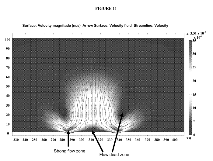
[0025] Figure 11 exemplifies the ACET flow pattern in the electrode chamber.
The magnitude
of the flow is depicted by color, where the strongest flow is seen a few
microns above the
chamber edge, while flow dead zones are located in the vortices center and in
the electrode ring
center, as indicated by the arrows. Stream lines exemplify the vortices formed
by the ACET
effect. Red arrows indicate flow direction.
[0026] Figure 12 exemplifiers a flow velocity profile (right) and a DEP
gradient (right)
generated by the microelectrode array with new floating electrode design.
DETAILED DESCRIPTION OF THE INVENTION
[0027] Described herein are methods, devices and systems suitable for
isolating or separating
nanoscale analytes from complex samples. In specific embodiments, provided
herein are
methods, devices and systems for isolating or separating a nanoscale analyte
from a sample
comprising other particulate material. In some aspects, the methods, devices
and systems may
allow for rapid separation of particles and nanoscale analytes in a sample. In
other aspects, the
methods, devices and systems may allow for rapid isolation of nanoscale
analytes from particles
in a sample. In various aspects, the methods, devices and systems may allow
for a rapid
procedure that requires a minimal amount of material and/or results in a
highly purified
nanoscale analyte isolated from complex fluids such as blood or environmental
samples.
[0028] Provided in certain embodiments herein are methods, devices and systems
for isolating
or separating nanoscale analytes from a sample, the methods, devices, and
systems comprising
applying the fluid to a device comprising an array of electrodes as disclosed
herein and being
capable of generating AC electrokinetic forces (e.g., when the array of
electrodes are energized).
- 7 -
CA 02945146 2016-10-06
WO 2015/157217 PCT/US2015/024624
AC Electrokinetics (ACE) capture is a functional relationship between the
dielectrophoretic
force (FDEp) and the flow force (FFLow) derived from the combination of AC
electrothermal
(ACET) and AC electroosmostic (ACE0) flows. In some embodiments, the
dielectrophoretic
field generated is a component of AC electrokinetic force effects. In other
embodiments, the
component of AC electrokinetic force effects is AC electroosmosis or AC
electrothermal effects.
In some embodiments the AC electrokinetic force, including dielectrophoretic
fields, comprises
high-field regions (positive DEP, i.e. area where there is a strong
concentration of electric field
lines due to a non-uniform electric field) and/or low-field regions (negative
DEP, i.e. area where
there is a weak concentration of electric field lines due to a non-uniform
electric field).
[0029] In specific instances, the nanoscale analytes (e.g., nucleic acid) are
isolated (e.g., isolated
or separated from particulate material) in a field region (e.g., a high field
region) of a
dielectrophoretic field. In some embodiments, the method, device, or system
includes isolating
and concentrating nanoscale analytes in a high field DEP region. In some
embodiments, the
method, device, or system includes isolating and concentrating nanoscale
analytes in a low field
DEP region The method also optionally includes devices and/or systems capable
of performing
one or more of the following steps: washing or otherwise removing residual
(e.g., cellular or
proteinaceous) material from the nanoscale analyte (e.g., rinsing the array
with water or buffer
while the nanoscale analyte is concentrated and maintained within a high field
DEP region of the
array), degrading residual proteins (e.g., degradation occurring according to
any suitable
mechanism, such as with heat, a protease, or a chemical), flushing degraded
proteins from the
nanoscale analyte, and collecting the nanoscale analyte. In some embodiments,
the result of the
methods, operation of the devices, and operation of the systems described
herein is an isolated
nanoscale analyte, optionally of suitable quantity and purity for further
analysis or
characterization in, for example, enzymatic assays (e.g. PCR assays).
[0030] In some embodiments, the methods, devices and compositions disclosed
herein utilize
electrode configurations and designs to improve separation and capture of the
nanoscale analytes
from particulate material. In some embodiments, the electrode arrays are
configured such that
fluid flow around or within the vicinity of the electrodes are disrupted or
altered, allowing the
localization and/or retention of nanoscale analytes around or within the
electrode arrays. In
other embodiments, the improvement in nanoscale analyte capture is at least
10%, at least 20%,
at least 30%, at least 40%, at least 50%, at least 60%, at least 70%, at least
80%, at least 90% or
at least 100% or more nanoscale analyte captured than if using conventional
electrode
configuration or designs, which do not have a reduction in conductive material
within the
electrodes.
- 8 -
CA 02945146 2016-10-06
WO 2015/157217 PCT/US2015/024624
[0031] In some embodiments, the array of electrodes as disclosed herein is
spin-coated with a
hydrogel having a thickness between about 0.1 microns and 1 micron. In some
embodiments, the
hydrogel is deposited onto the array of electrodes by chemical vapor
deposition or surface-
initiated polymerization. In yet other embodiments, the hydrogel is deposited
onto the array of
electrodes by dip coating, spray coating, inkjet printing, Langmuir-Blodgett
coating, or
combinations thereof. In still other embodiments, the hydrogel is deposited
onto the array of
electrodes by grafting of polymers by end-functionalized groups or by self-
assembly from
solution thru solvent selectivity. In some embodiments, the hydrogel comprises
two or more
layers of a synthetic polymer. In some embodiments, the hydrogel has a
viscosity between about
0.5 cP to about 5 cP prior to spin-coating or deposition onto the array of
electrodes. In some
embodiments, the hydrogel has a conductivity between about 0.1 S/m to about
1.0 S/m.
[0032] In some embodiments, the isolated nanoscale analyte comprises less than
about 10%
non-nanoscale analyte by mass. In some embodiments, the method is completed in
less than 10
minutes.
[0033] In some embodiments, the method further comprises degrading residual
proteins on the
array. In some embodiments, the residual proteins are degraded by one or more
of a chemical
degradant or an enzymatic degradant. In some embodiments, the residual
proteins are degraded
by Proteinase K.
[0034] In some embodiments, the nanoscale analyte is a nucleic acid. In other
embodiments, the
nucleic acid is further amplified by polymerase chain reaction. In some
embodiments, the
nucleic acid comprises DNA, RNA, or any combination thereof. In some
embodiments, the
isolated nucleic acid comprises less than about 80%, less than about 70%, less
than about 60%,
less than about 50%, less than about 40%, less than about 30%, less than about
20%, less than
about 10%, less than about 5%, or less than about 2% non-nucleic acid cellular
material and/or
protein by mass. In some embodiments, the isolated nucleic acid comprises
greater than about
99%, greater than about 98%, greater than about 95%, greater than about 90%,
greater than
about 80%, greater than about 70%, greater than about 60%, greater than about
50%, greater
than about 40%, greater than about 30%, greater than about 20%, or greater
than about 10%
nucleic acid by mass. In some embodiments, the method is completed in less
than about one
hour. In some embodiments, centrifugation is not used. In some embodiments,
the residual
proteins are degraded by one or more of chemical degradation and enzymatic
degradation. In
some embodiments, the residual proteins are degraded by Proteinase K. In some
embodiments,
the residual proteins are degraded by an enzyme, the method further comprising
inactivating the
enzyme following degradation of the proteins. In some embodiments, the enzyme
is inactivated
by heat (e.g., 50 to 95 C for 5 ¨ 15 minutes). In some embodiments, the
residual material and
- 9 -
CA 02945146 2016-10-06
WO 2015/157217 PCT/US2015/024624
the degraded proteins are flushed in separate or concurrent steps. In some
embodiments, the
isolated nanoscale analyte is collected by (i) turning off the second AC
electrokinetic field
region; and (ii) eluting the nanoscale analyte from the array in an eluant. In
some embodiments,
a nanoscale analyte is isolated in a form suitable for sequencing. In some
embodiments, the
nanoscale analyte is isolated in a fragmented form suitable for shotgun-
sequencing.
[0035] In some embodiments, the nucleic acid is sequenced by Sanger
sequencing,
pyrosequencing, ion semiconductor sequencing, polony sequencing, sequencing by
ligation,
DNA nanoball sequencing, sequencing by ligation, or single molecule
sequencing. In some
embodiments, the method further comprises performing a reaction on the DNA
(e.g.,
fragmentation, restriction digestion, ligation) that is isolated and eluted
from the devices
disclosed herein. In some embodiments, the reaction occurs on or near the
array or in the device.
In some embodiments, the fluid or biological sample comprises no more than
10,000 cells.
[0036] In some embodiments, the sample is a biological sample and has a low
conductivity or a
high conductivity. In some embodiments, the sample comprises a bodily fluid,
blood, serum,
plasma, urine, saliva, a food, a beverage, a growth medium, an environmental
sample, a liquid,
water, clonal cells, or a combination thereof. In some embodiments, the cells
comprise clonal
cells, pathogen cells, bacteria cells, viruses, plant cells, animal cells,
insect cells, and/or
combinations thereof.
[0037] In some embodiments, the devices and methods disclosed herein further
comprises using
at least one of an elution tube, a chamber and a reservoir to perform
amplification of isolated
nucleic acids as the nanoscale analyte. In some embodiments, amplification of
the isolated and
eluted nucleic acid is polymerase chain reaction (PCR)-based. In some
embodiments,
amplification of the nucleic acid is performed in a serpentine microchannel
comprising a
plurality of temperature zones. In some embodiments, amplification is
performed in aqueous
droplets entrapped in immiscible fluids (i.e., digital PCR). In some
embodiments, the
thermocycling comprises convection. In some embodiments, the device comprises
a surface
contacting or proximal to the electrodes, wherein the surface is
functionalized with biological
ligands that are capable of selectively capturing biomolecules. In some
embodiments, the
surface selectively captures biomolecules by: a.nucleic acid hybridization; b.
antibody - antigen
interactions; c. biotin - avidin interactions; d. ionic or electrostatic
interactions; or e. any
combination thereof. In some embodiments, the surface is functionalized to
minimize and/or
inhibit nonspecific binding interactions by: a. polymers (e.g., polyethylene
glycol PEG); b. ionic
or electrostatic interactions; c.surfactants; or d. any combination thereof.
In some embodiments,
the device comprises a plurality of microelectrode devices oriented (a) flat
side by side, (b)
facing vertically, or (c) facing horizontally. In some embodiments, the device
comprises a
- 10 -
CA 02945146 2016-10-06
WO 2015/157217 PCT/US2015/024624
module capable of performing Sanger sequencing. In some embodiments, the
module capable of
performing Sanger sequencing comprises a module capable of capillary
electrophoresis, a
module capable of multi-color fluorescence detection, or a combination
thereof.
[0038] In some instances, it is advantageous that the methods described herein
are performed in
a short amount of time, the devices are operated in a short amount of time,
and the systems are
operated in a short amount of time. In some embodiments, the period of time is
short with
reference to the "procedure time" measured from the time between adding the
fluid to the device
and obtaining isolated nanoscale analyte. In some embodiments, the procedure
time is less than
3 hours, less than 2 hours, less than 1 hour, less than 30 minutes, less than
20 minutes, less than
minutes, or less than 5 minutes.
[0039] In another aspect, the period of time is short with reference to the
"hands-on time"
measured as the cumulative amount of time that a person must attend to the
procedure from the
time between adding the fluid to the device and obtaining isolated nanoscale
analyte. In some
embodiments, the hands-on time is less than 20 minutes, less than 10 minutes,
less than 5
minute, less than 1 minute, or less than 30 seconds.
[0040] In some instances, it is advantageous that the devices described herein
comprise a single
vessel, the systems described herein comprise a device comprising a single
vessel and the
methods described herein can be performed in a single vessel, e.g., in a
dielectrophoretic device
as described herein. In some aspects, such a single-vessel embodiment
minimizes the number of
fluid handling steps and/or is performed in a short amount of time. In some
instances, the
present methods, devices and systems are contrasted with methods, devices and
systems that use
one or more centrifugation steps and/or medium exchanges. In some instances,
centrifugation
increases the amount of hands-on time required to isolate nanoscale analytes.
In another aspect,
the single-vessel procedure or device isolates nanoscale analytes using a
minimal amount of
consumable reagents.
Devices and Systems
[0041] In some embodiments, described herein are devices for isolating,
purifying and
collecting a nanoscale analyte from a sample. In one aspect, described herein
are devices for
isolating, purifying and collecting or eluting a nanoscale from a complex
sample other
particulate material, including cells and the like. In other aspects, the
devices disclosed herein
are capable of isolating, purifying, collecting and/or eluting nanoscale
analytes from a sample
comprising cellular or protein material. In yet other aspects, the devices
disclosed herein are
capable of isolating, purifying, collecting and/or eluting nanoscale analytes
from samples
comprising a complex mixture of organic and inorganic materials. In some
aspects, the devices
disclosed herein are capable of isolating, purifying, collecting and/or
eluting nanoscale analytes
-11-
CA 02945146 2016-10-06
WO 2015/157217 PCT/US2015/024624
from samples comprising organic materials. In yet other aspects, the devices
disclosed herein
are capable of isolating, purifying, collecting and/or eluting nanoscale
analytes from samples
comprising inorganic materials.
[0042] In some embodiments, disclosed herein is a device for isolating a
nanoscale analyte in a
sample, the device comprising: a. a housing; b. a heater and/or a reservoir
comprising a protein
degradation agent; and c. a plurality of alternating current (AC) electrodes
as disclosed herein
within the housing, the AC electrodes configured to be selectively energized
to establish AC
electrokinetic high field and AC electrokinetic low field regions, wherein the
electrodes
comprise conductive material configured on or around the electrodes which
reduces, disrupts or
alters fluid flow around or within the vicinity of the electrodes as compared
to fluid flow in
regions between or substantially beyond the electrode vicinity. In some
embodiments, the
conductive material is substantially absent from the center of the individual
electrodes in the
array. In some embodiments, the conductive material is present at the edges of
the individual
electrodes in the electrode array.
[0043] In some embodiments, an AC electrokinetic field is generated to
collect, separate or
isolate nanoscale analytes. In some embodiments, the nanoscale analytes are
biomolecules, such
as nucleic acids. In some embodiments, the AC electrokinetic field is a
dielectrophoretic field.
Accordingly, in some embodiments dielectrophoresis (DEP) is utilized in
various steps of the
methods and devices described herein.
[0044] Accordingly provided herein are systems and devices comprising a
plurality of
alternating current (AC) electrodes as disclosed herein, the AC electrodes
configured to be
selectively energized to establish a dielectrophoretic (DEP) field region. In
some aspects, the
AC electrodes may be configured to be selectively energized to establish
multiple
dielectrophoretic (DEP) field regions, including dielectrophoretic (DEP) high
field and
dielectrophoretic (DEP) low field regions. In some instances, AC
electrokinetic effects provide
for concentration of larger particulate material in low field regions and/or
concentration (or
collection or isolation) of nanoscale analytes (e.g., macromolecules, such as
nucleic acid) in high
field regions of the DEP field. For example, further description of the
electrodes and the
concentration of cells in DEP fields may be found in PCT patent publication WO
2009/146143
A2, which is incorporated herein for such disclosure.
[0045] In specific embodiments, DEP is used to concentrate nanoscale analytes
and larger
particulate matter either concurrently or at different times. In certain
embodiments, methods and
devices described herein are capable of energizing the array of electrodes as
disclosed herein so
as to produce at least one DEP field. In other embodiments, the methods and
devices described
here further comprise energizing the array of electrodes so as to produce a
first, second, and any
- 12 -
CA 02945146 2016-10-06
WO 2015/157217 PCT/US2015/024624
further optional DEP fields. In some embodiments, the devices and systems
described herein are
capable of being energized so as to produce a first, second, and any further
optional DEP fields.
[0046] DEP is a phenomenon in which a force is exerted on a dielectric
particle when it is
subjected to a non-uniform electric field. Depending on the step of the
methods described
herein, aspects of the devices and systems described herein, and the like, the
dielectric particle in
various embodiments herein is a biological nanoscale analyte, such as a
nucleic acid molecule.
Different steps of the methods described herein or aspects of the devices or
systems described
herein may be utilized to isolate and separate different components, such as
intact cells or other
particular material; further, different field regions of the DEP field may be
used in different
steps of the methods or aspects of the devices and systems described herein.
The
dielectrophoretic force generated in the device does not require the particle
to be charged. In
some instances, the strength of the force depends on the medium and the
specific particles'
electrical properties, on the particles' shape and size, as well as on the
frequency of the electric
field. In some instances, fields of a particular frequency selectively
manipulate particles. In
certain aspects described herein, these processes allow for the separation of
nanoscale analytes,
including nucleic acid molecules, from other components, such as cells and
proteinaceous
material.
[0047] Also provided herein are systems and devices comprising a plurality of
direct current
(DC) electrodes. In some embodiments, the plurality of DC electrodes comprises
at least two
rectangular electrodes, spread throughout the array. In some embodiments, the
electrodes are
located at the edges of the array. In some embodiments, DC electrodes are
interspersed between
AC electrodes.
[0048] In some embodiments, disclosed herein is a device for isolating a
nanoscale analyte in a
sample, the device comprising: (1) a housing; (2) a plurality of alternating
current (AC)
electrodes as disclosed herein within the housing, the AC electrodes
configured to be selectively
energized to establish AC electrokinetic high field and AC electrokinetic low
field regions,
whereby AC electrokinetic effects provide for concentration of the nanoscale
analytes cells in an
electrokinetic field region of the device. In some embodiments, the plurality
of electrodes is
configured to be selectively energized to establish a dielectrophoretic high
field and
dielectrophoretic low field regions.
[0049] In some embodiments, disclosed herein is a device comprising: (1) a
plurality of
alternating current (AC) electrodes as disclosed herein, the AC electrodes
configured to be
selectively energized to establish AC electrokinetic high field and AC
electrokinetic low field
regions; and (2) a module capable of performing enzymatic reactions, such as
polymerase chain
reaction (PCR) or other enzymatic reaction. In some embodiments, the plurality
of electrodes is
- 13 -
CA 02945146 2016-10-06
WO 2015/157217 PCT/US2015/024624
configured to be selectively energized to establish a dielectrophoretic high
field and
dielectrophoretic low field regions. In some embodiments, the device is
capable of isolating a
nanoscale analyte from a sample, collecting or eluting the nanoscale analyte
and further
performing an enzymatic reaction on the nanoscale analyte. In some
embodiments, the
enzymatic reaction is performed in the same chamber as the isolation and
elution stages. In
other embodiments, the enzymatic reaction is performed in another chamber than
the isolation
and elution stages. In still other embodiments, a nanoscale analyte is
isolated and the enzymatic
reaction is performed in multiple chambers.
[0050] In some embodiments, the device further comprises at least one of an
elution tube, a
chamber and a reservoir to perform an enzymatic reaction. In some embodiments,
the enzymatic
reaction is performed in a serpentine microchannel comprising a plurality of
temperature zones.
In some embodiments, the enzymatic reaction is performed in aqueous droplets
entrapped in
immiscible fluids (e.g., digital PCR). In some embodiments, the thermal
reaction comprises
convection. In some embodiments, the device comprises a surface contacting or
proximal to the
electrodes, wherein the surface is functionalized with biological ligands that
are capable of
selectively capturing biomolecules.
[0051] In one aspect, described herein is a device comprising electrodes,
wherein the electrodes
are placed into separate chambers and DEP fields are created within an inner
chamber by
passage through pore structures. The exemplary device includes a plurality of
electrodes and
electrode-containing chambers within a housing. A controller of the device
independently
controls the electrodes, as described further in PCT patent publication WO
2009/146143 A2,
which is incorporated herein for such disclosure.
[0052] In some embodiments, chambered devices are created with a variety of
pore and/or hole
structures (nanoscale, microscale and even macroscale) and contain membranes,
gels or filtering
materials which control, confme or prevent cells, nanoparticles or other
entities from diffusing
or being transported into the inner chambers while the AC/DC electric fields,
solute molecules,
buffer and other small molecules can pass through the chambers.
[0053] Such devices include, but are not limited to, multiplexed electrode and
chambered
devices, devices that allow reconfigurable electric field patterns to be
created, devices that
combine DC electrophoretic and fluidic processes; sample preparation devices,
sample
preparation, enzymatic manipulation of isolated nucleic acid molecules and
diagnostic devices
that include subsequent detection and analysis, lab-on-chip devices, point-of-
care and other
clinical diagnostic systems or versions.
[0054] In some embodiments, a planar electrode array device comprises a
housing through
which a sample fluid flows. In some embodiments, fluid flows from an inlet end
to an outlet
- 14 -
CA 02945146 2016-10-06
WO 2015/157217 PCT/US2015/024624
end, optionally comprising a lateral analyte outlet. The exemplary device
includes multiple AC
electrodes. In some embodiments, the sample consists of a combination of
micron-sized entities
or cells, larger nanoscale analytes and smaller nanoscale analytes or
biomolecules.
[0055] In some embodiments, the smaller nanoscale analytes are proteins,
smaller DNA, RNA
and cellular fragments. In some embodiments, the planar electrode array device
is a 60x20
electrode array that is optionally sectioned into three 20x20 arrays that can
be separately
controlled but operated simultaneously. The optional auxiliary DC electrodes
can be switched on
to positive charge, while the optional DC electrodes are switched on to
negative charge for
electrophoretic purposes. In some instances, each of the controlled AC and DC
systems is used
in both a continuous and/or pulsed manner (e.g., each can be pulsed on and off
at relatively short
time intervals) in various embodiments. The optional planar electrode arrays
along the sides of
the sample flow are optionally used to generate DC electrophoretic forces as
well as AC DEP.
Additionally, microelectrophoretic separation processes may be optionally
carried out, in
combination with nanopore or hydrogel layers on the electrode array, using
planar electrodes in
the array and/or auxiliary electrodes in the x-y-z dimensions.
[0056] In various embodiments these methods, devices and systems are operated
in the AC
frequency range of from 1,000 Hz to 100 MHz, at voltages which could range
from
approximately 1 volt to 2000 volts pk-pk; at DC voltages from 1 volt to 1000
volts, at flow rates
of from 10 microliters per minute to 10 milliliter per minute, and in
temperature ranges from 1
C to 120 C. In some embodiments, the methods, devices and systems are
operated in AC
frequency ranges of from about 3 to about 15 kHz. In some embodiments, the
methods, devices,
and systems are operated at voltages of from 5-25 volts pk-pk. In some
embodiments, the
methods, devices and systems are operated at voltages of from about 1 to about
50 volts/cm. In
some embodiments, the methods, devices and systems are operated at DC voltages
of from
about 1 to about 5 volts. In some embodiments, the methods, devices and
systems are operated
at a flow rate of from about 10 microliters to about 500 microliters per
minute. In some
embodiments, the methods, devices and systems are operated in temperature
ranges of from
about 20 C to about 60 C.
[0057] In some embodiments, the methods, devices and systems are operated in
AC frequency
ranges of from 1,000 Hz to 10 MHz. In some embodiments, the methods, devices
and systems
are operated in AC frequency ranges of from 1,000 Hz to 1 MHz. In some
embodiments, the
methods, devices and systems are operated in AC frequency ranges of from 1,000
Hz to 100
kHz. In some embodiments, the methods, devices and systems are operated in AC
frequency
ranges of from 1,000 Hz to 10 kHz. In some embodiments, the methods, devices
and systems
- 15 -
CA 02945146 2016-10-06
WO 2015/157217 PCT/US2015/024624
are operated in AC frequency ranges of from 10 kHz to 100 kHz. In some
embodiments, the
methods, devices and systems are operated in AC frequency ranges of from 100
kHz to 1 MHz.
[0058] In some embodiments, the methods, devices and systems are operated at
voltages from
approximately 1 volt to 1500 volts pk-pk. In some embodiments, the methods,
devices and
systems are operated at voltages from approximately 1 volt to 1500 volts pk-
pk. In some
embodiments, the methods, devices and systems are operated at voltages from
approximately 1
volt to 1000 volts pk-pk. In some embodiments, the methods, devices and
systems are operated
at voltages from approximately 1 volt to 500 volts pk-pk. In some embodiments,
the methods,
devices and systems are operated at voltages from approximately 1 volt to 250
volts pk-pk. In
some embodiments, the methods, devices and systems are operated at voltages
from
approximately 1 volt to 100 volts pk-pk. In some embodiments, the methods,
devices and
systems are operated at voltages from approximately 1 volt to 50 volts pk-pk.
[0059] In some embodiments, the methods, devices and systems are operated at
DC voltages
from 1 volt to 1000 volts. In some embodiments, the methods, devices and
systems are operated
at DC voltages from 1 volt to 500 volts. In some embodiments, the methods,
devices and
systems are operated at DC voltages from 1 volt to 250 volts. In some
embodiments, the
methods, devices and systems are operated at DC voltages from 1 volt to 100
volts. In some
embodiments, the methods, devices and systems are operated at DC voltages from
1 volt to 50
volts.
[0060] In some embodiments, the AC electrokinetic field is produced using an
alternating
current having a voltage of 1 volt to 40 volts peak-peak, and/or a frequency
of 5 Hz to 5,000,000
Hz and duty cycles from 5% to 50%.
[0061] In some embodiments, the methods, devices, and systems are operated at
flow rates of
from 10 microliters per minute to 1 ml per minute. In some embodiments, the
methods, devices,
and systems are operated at flow rates of from 10 microliters per minute to
500 microliters per
minute. In some embodiments, the methods, devices, and systems are operated at
flow rates of
from 10 microliters per minute to 250 microliters per minute. In some
embodiments, the
methods, devices, and systems are operated at flow rates of from 10
microliters per minute to
100 microliters per minute.
[0062] In some embodiments, the methods, devices, and systems are operated in
temperature
ranges from 1 C to 100 C. In some embodiments, the methods, devices, and
systems are
operated in temperature ranges from 20 C to 95 C. In some embodiments, the
methods,
devices, and systems are operated in temperature ranges from 25 C to 100 C.
In some
embodiments, the methods, devices, and systems are operated at room
temperature.
- 16 -
CA 02945146 2016-10-06
WO 2015/157217 PCT/US2015/024624
[0063] In some embodiments, the controller independently controls each of the
electrodes. In
some embodiments, the controller is externally connected to the device such as
by a socket and
plug connection, or is integrated with the device housing.
[0064] In some embodiments, the device comprises a housing and a heater or
thermal source
and/or a reservoir comprising a protein degradation agent. In some
embodiments, the heater or
thermal source is capable of increasing the temperature of the fluid to a
desired temperature
(e.g., to a temperature suitable for degrading proteins, about 30 C, 40 C,
50 C, 60 C, 70 C,
or the like). In some embodiments, the heater or thermal source is suitable
for operation as a
PCR thermocycler. In other embodiments, the heater or thermal source is used
to maintain a
constant temperature (isothermal conditions). In some embodiments, the protein
degradation
agent is a protease. In other embodiments, the protein degradation agent is
Proteinase K and the
heater or thermal source is used to inactivate the protein degradation agent.
[0065] In some embodiments, the device comprises a second reservoir comprising
an eluant.
The eluant is any fluid suitable for eluting the isolated nanoscale analyte
from the device. In
some instances the eluant is water or a buffer. In some instances, the eluant
comprises reagents
required for a DNA sequencing method.
[0066] In some embodiments, a system or device described herein is capable of
maintaining a
constant temperature. In some embodiments, a system or device described herein
is capable of
cooling the array or chamber. In some embodiments, a system or device
described herein is
capable of heating the array or chamber. In some embodiments, a system or
device described
herein comprises a thermocycler. In some embodiments, the devices disclosed
herein comprise
a localized temperature control element. In some embodiments, the devices
disclosed herein are
capable of both sensing and controlling temperature.
[0067] In some embodiments, the devices further comprise heating or thermal
elements. In
some embodiments, a heating or thermal element is localized underneath an
electrode. In some
embodiments, the heating or thermal elements comprise a metal. In some
embodiments, the
heating or thermal elements comprise tantalum, aluminum, tungsten, or a
combination thereof.
Generally, the temperature achieved by a heating or thermal element is
proportional to the
current running through it. In some embodiments, the devices disclosed herein
comprise
localized cooling elements. In some embodiments, heat resistant elements are
placed directly
under the exposed electrode array. In some embodiments, the devices disclosed
herein are
capable of achieving and maintaining a temperature between about 20 C and
about 120 C. In
some embodiments, the devices disclosed herein are capable of achieving and
maintaining a
temperature between about 30 C and about 100 C. In other embodiments, the
devices disclosed
herein are capable of achieving and maintaining a temperature between about 20
C and about
- 17 -
CA 02945146 2016-10-06
WO 2015/157217 PCT/US2015/024624
95 C. In some embodiments, the devices disclosed herein are capable of
achieving and
maintaining a temperature between about 25 C and about 90 C, between about 25
C and about
85 C, between about 25 C and about 75 C, between about 25 C and about 65
C or between
about 25 C and about 55 C. In some embodiments, the devices disclosed herein
are capable of
achieving and maintaining a temperature of about 20 C, about 30 C, about 40
C, about 50 C,
about 60 C, about 70 C, about 80 C, about 90 C, about 100 C, about 110 C
or about 120 C.
Electrodes
[0068] In some embodiments, the methods, devices and compositions disclosed
herein utilize
electrode configurations and designs to improve separation and capture of the
nanoscale analytes
from particulate material. In some embodiments, the electrode arrays are
configured such that
fluid flow around or within the vicinity of the electrodes are disrupted or
altered, allowing the
localization and/or retention of nanoscale analytes around or within the
electrode arrays. In
other embodiments, the improvement in nanoscale analyte capture is at least
10%, at least 20%,
at least 30%, at least 40%, at least 50%, at least 60%, at least 70%, at least
80%, at least 90% or
at least 100% or more nanoscale analyte captured than if using conventional
electrode
configuration or designs.
[0069] In some embodiments, the conductive material is in the shape of an open
disk. In some
embodiments, the electrode is configured in a hollow ring shape. In some
embodiments, the
electrode is configured in a hollow tube shape. In some embodiments, the array
of electrodes as
disclosed herein comprises non-conductive material. In some embodiments, the
non-conductive
material surrounds the conductive material within the electrodes and serves as
a physical barrier
to the conductive material. In some embodiments, the conductive material
within the electrodes
fills depressions in the non-conductive material of the array. In some
embodiments, the array of
electrodes as disclosed herein is configured in three-dimensions.
[0070] In one embodiment, the array of electrodes as disclosed herein
comprises conductive
material in only a fraction of the electrode array. In some embodiments, the
conductive material
is only present in less than about 10% of the electrode array. In some
embodiments, the
conductive material is only present in about 10% of the electrode array. In
other embodiments,
the conductive material is only present in about 20% of the electrode array.
In still other
embodiments, the conductive material is only present in about 30% of the
electrode array. In yet
other embodiments, the conductive material is only present in about 40% of the
electrode array.
In still other embodiments, the conductive material is only present in about
50% of the electrode
array. In some embodiments, the conductive material is only present in about
60% of the
electrode array. In one embodiment, the conductive material is only present in
about 70% of the
electrode array. In still other embodiments, the conductive material is only
present in about 80%
- 18 -
CA 02945146 2016-10-06
WO 2015/157217 PCT/US2015/024624
of the electrode array. In yet other embodiments, the conductive material is
only present in
about 90% of the electrode array.
[0071] In still other embodiments, the conductive material is only present in
about 10%, in
about 15%, in about 20%, in about 25%, in about 30%, in about 35%, in about
40%, in about
45%, in about 50%, in about 55%, in about 60%, in about 65%, in about 70%, in
about 75%, in
about 80%, in about 85% and in about 90% of the electrode array. In yet other
embodiments,
the conductive material is present in about 10-70% of the electrode array, in
about 10-60% of
the electrode array, in about 10-50% of the electrode array, in about 10-40%
of the electrode or
in about 10-30% of the electrode array. In other embodiments, the conductive
material is
present in about 30-90% of the electrode array, in about 30-80% of the
electrode array, in about
30-70% of the electrode array, in about 30-60% of the electrode array or in
about 30-50% of the
electrode array. In some embodiments, the conductive material is present in
about 8 to about
40% of the electrode array.
[0072] In yet other embodiments, the conductive material is substantially
absent from the center
of the individual electrodes in the electrode array. In other embodiments, the
conductive
material is only present at the edges of the individual electrodes in the
electrode array. In still
other embodiments, the conductive material is in the shape of an open disk,
which comprises
conductive material that is discontinuous in the open disk electrode. In some
embodiments, the
electrode is a hollow ring electrode shape, which comprises conductive
material in the electrode
array that is substantially absent from the center of the individual
electrodes or is only at the
edge of the individual electrodes. The hollow ring electrode shape, like the
open disk shape,
reduces the surface area of the conductive material in an electrode. The
reduction in conductive
material present on the electrode results in flow in and around the electrode
surface, leading to
increases in nanoscale analyte captured on the surface of the electrode.
[0073] In some embodiments, a layer of non-conductive material is present in
certain areas of
the electrode or in the proximal vicinity of the electrode array. In one
embodiment, a layer of
non-conductive material surrounds the electrode array, creating a physical
barrier or wall
surrounding the array. In some embodiments, the electrode array is depressed
into the array
material, creating a well or depression on the array surface wherein electrode
material or
substantially electrode material is present in the well or depression.
[0074] In some embodiments, the electrode configuration is in three-
dimensions. In some
embodiments, the electrode material is folded into an angle configuration. In
other
embodiments, the electrode material is formed into a triangular tube. In other
embodiments, the
electrode material is formed into a hollow triangular tube. In still other
embodiments, the three
dimensional electrode comprises angles between neighboring planar electrode
surfaces of less
- 19 -
CA 02945146 2016-10-06
WO 2015/157217 PCT/US2015/024624
than about 180 degrees, less than about 170 degrees, less than about 160
degrees, less than about
150 degrees, less than about 140 degrees, less than about 130 degrees, less
than about 120
degrees, less than about 110 degrees, less than about 100 degrees, less than
about 90 degrees,
less than about 80 degrees, less than about 70 degrees, but not less than
about 60 degrees. In
some embodiments, the conductive material configured into angles between
neighboring planar
electrode surfaces of equal to or less than 180 degrees. In some embodiments,
the three
dimensional electrode configuration comprises angles between neighboring
planar electrode
surfaces of more than about 60 degrees, more than about 70 degrees, more than
about 80
degrees, more than about 90 degrees, more than about 100 degrees, more than
about 110
degrees, more than about 120 degrees, more than about 130 degrees, more than
about 140
degrees, more than about 150 degrees, more than about 160 degrees, more than
about 170
degrees, but not more than about 180 degrees. In some embodiments, the
conductive material
configured into angles between neighboring planar electrode surfaces of equal
to or more than
60 degrees. In some embodiments, the conductive material within the electrodes
is configured
into a depressed concave shape. In yet other embodiments, the electrode
configuration is a
depressed basket electrode. The three-dimensional structure of the electrode
increases the total
surface area of the electrode, allowing interrogation of more fluid in a
defined unit of time.
[0075] In some embodiments, the individual electrodes are about 40 gm to about
100 gm in
diameter. In still other embodiments, the individual electrodes are about 40
gm, about 45 gm,
about 50 gm, about 55 gm, about 60 gm, about 65 gm, about 70 gm, about 75 gm,
about 80 gm,
about 85 gm, about 90 gm, about 95 gm or about 100 gm in diameter. In yet
other
embodiments, the individual electrodes are about 40 gm to about 50 gm, about
40 gm to about
60 gm or about 40 gm to about 70 gm. In still other embodiments, the
individual electrodes are
about 100 gm, about 200 gm, about 300 gm, about 400 gm, about 500 gm, about
600 gm, about
700 gm, about 800 gm, about 900 gm, or about 1000 gm in diameter.
[0076] The plurality of alternating current electrodes are optionally
configured in any manner
suitable for the separation processes described herein. In other embodiments,
the array of
electrodes as disclosed herein comprises a pattern of electrode
configurations, wherein the
configuration comprises a repeating unit of electrode arrays. In some
embodiments, the edge to
edge distance between a parallel set of repeating units is equidistant, or
roughly equidistant.
Further description of the system or device including electrodes and/or
concentration of cells in
DEP fields is found in PCT patent publication WO 2009/146143, which is
incorporated herein
for such disclosure.
[0077] In some embodiments, the electrodes disclosed herein comprise any
suitable metal. In
other embodiments, the electrodes disclosed herein comprise a noble metal. In
some
- 20 -
CA 02945146 2016-10-06
WO 2015/157217 PCT/US2015/024624
embodiments, the electrodes can include but are not limited to: aluminum,
copper, carbon, iron,
silver, gold, palladium, platinum, iridium, platinum iridium alloy, ruthenium,
rhodium, osmium,
tantalum, titanium, tungsten, polysilicon, and indium tin oxide, or
combinations thereof, as well
as silicide materials such as platinum silicide, titanium silicide, gold
silicide, or tungsten silicide.
In some embodiments, the electrodes can comprise a conductive ink capable of
being screen-
printed. In some embodiments, the electrodes comprise a conductive polymer,
such as
polyacetylene or polythiophene.
[0078] In one embodiment, the electrode material is about 100 to about 1000 nm
thick. In some
embodiments, the electrode material is about 200 to about 800 nm thick. In yet
other
embodiments, the electrode material is about 300 to about 500 nm thick. In
still other
embodiments, the electrode material is about 100 nm, about 150 nm, about 200
nm, about 250
nm, about 300 nm, about 350 nm, about 400 nm, about 450 nm, about 500 nm,
about 550 nm,
about 600 nm, about 650 nm, about 700 nm, about 750 nm, about 800 nm, about
850 nm, about
900 nm, about 950 nm or about 1000 nm thick.
[0079] In some embodiments, an adhesion layer is deposited or printed onto the
array as a
protective layer prior to deposition of the electrode material. In some
embodiments, the
adhesion layer comprises any suitable material. In one embodiment, the
adhesion layer
comprises titanium or tungsten. In other embodiments, the adhesion layer is
between about 10
to about 50 nm thick. In some embodiments, the adhesion layer is between about
20 to about 40
nm thick. In yet other embodiments, the adhesion layer is between about 20 to
about 30 nm
thick. In still other embodiments, the adhesion layer is about 10 nm, about 20
nm, about 30 nm,
about 40 nm or about 50 nm thick.
[0080] In some embodiments, the edge to edge (E2E) to diameter ratio of an
individual
electrode is about 10 gm to about 500 gm. In some embodiments, the E2E of an
electrode is
about 50 gm to about 300 gm. In yet other embodiments, the E2E of an electrode
is about 100
gm to about 200 gm. In still other embodiments, the E2E of an electrode is
about 50 gm, about
60 gm, about 70 gm, about 80 gm, about 90 gm, about 100 gm, about 110 gm,
about 120 gmm
about 130 gm, about 140 gm, about 150 gm, about 160 gm, about 170 gm, about
180 gm, about
190 gm, about 200 gm, about 210 gm, about 220 gm, about 230 gm, about 240 gm,
about 250
gm, about 260 gm, about 270 gm, about 280 gm, about 290 gm, about 300 gm,
about 310 gm,
about 320 gm, about 330 gm, about 340 gm, about 350 gm, about 360 gm, about
370 gm, about
380 gm, about 390 gm, about 400 gm, about 410 gm, about 420 gm, about 430 gm,
about 440
gm, about 450 gm, about 460 gm, about 470 gm, about 480 gm, about 490 gm or
about 500
gm. In some embodiments, the E2E of an electrode is about 750 gm, about 1000
gm, about
1500 gm, or about 2000 gm.
-21-
CA 02945146 2016-10-06
WO 2015/157217 PCT/US2015/024624
[0081] In some embodiments, the electrodes disclosed herein are dry-etched. In
some
embodiments, the electrodes are wet etched. In some embodiments, the
electrodes undergo a
combination of dry etching and wet etching.
[0082] In some embodiments, each electrode is individually site-controlled.
[0083] In some embodiments, an array of electrodes as disclosed herein is
controlled as a unit.
[0084] The array can be of any suitable material. In some embodiments, the
array comprises
plastic or silica. In some embodiments, the array comprises silicon dioxide.
In some
embodiments, the array comprises aluminum.
[0085] In some embodiments, a passivation layer is employed. In some
embodiments, a
passivation layer can be formed from any suitable material known in the art.
In some
embodiments, the passivation layer comprises silicon nitride. In some
embodiments, the
passivation layer comprises silicon dioxide. In some embodiments, the
passivation layer has a
relative electrical permittivity of from about 2.0 to about 8Ø In some
embodiments, the
passivation layer has a relative electrical permittivity of from about 3.0 to
about 8.0, about 4.0 to
about 8.0 or about 5.0 to about 8Ø In some embodiments, the passivation
layer has a relative
electrical permittivity of about 2.0 to about 4Ø In some embodiments, the
passivation layer has
a relative electrical permittivity of from about 2.0 to about 3Ø In some
embodiments, the
passivation layer has a relative electrical permittivity of about 2.0, about
2.5, about 3.0, about
3.5 or about 4Ø
[0086] In some embodiments, the passivation layer is between about 0.1 microns
and about 10
microns in thickness. In some embodiments, the passivation layer is between
about 0.5 microns
and 8 microns in thickness. In some embodiments, the passivation layer is
between about 1.0
micron and 5 microns in thickness. In some embodiments, the passivation layer
is between
about 1.0 micron and 4 microns in thickness. In some embodiments, the
passivation layer is
between about 1.0 micron and 3 microns in thickness. In some embodiments, the
passivation
layer is between about 0.25 microns and 2 microns in thickness. In some
embodiments, the
passivation layer is between about 0.25 microns and 1 micron in thickness.
[0087] In some embodiments, the passivation layer is comprised of any suitable
insulative low k
dielectric material, including but not limited to silicon nitride, silicon
dioxide or titanium
dioxide. In some embodiments, the passivation layer is chosen from the group
consisting of
polyamids, carbon, doped silicon nitride, carbon doped silicon dioxide,
fluorine doped silicon
nitride, fluorine doped silicon dioxide, porous silicon dioxide, or any
combinations thereof. In
some embodiments, the passivation layer can comprise a dielectric ink capable
of being screen-
printed.
- 22 -
CA 02945146 2016-10-06
WO 2015/157217 PCT/US2015/024624
Electrode Geometry
[0088] In some embodiments, the electrodes disclosed herein can be arranged in
any manner
suitable for practicing the methods disclosed herein.
[0089] In various embodiments, a variety of configurations for the devices are
possible. For
example, a device comprising a larger array of electrodes, for example in a
square or rectangular
pattern configured to create a repeating non-uniform electric field to enable
AC electrokinetics.
For illustrative purposes only, a suitable electrode array may include, but is
not limited to, a
10x10 electrode configuration, a 50x50 electrode configuration, al Ox100
electrode
configuration, 20x100 electrode configuration, or a 20x80 electrode
configuration.
[0090] In some embodiments, the electrodes are in a dot configuration, e.g.
the electrodes
comprises a generally circular or round configuration (see, e.g., Figures 1 &
2). In some
embodiments, the electrodes are configured as disks. In some embodiments, the
electrodes are
configured as rings. In some embodiments, the angle of orientation between
dots is from about
30 to about 90 degrees. In some embodiments, the angle of orientation
between dots is from
about 25 to about 60 . In some embodiments, the angle of orientation between
dots is from
about 300 to about 55 . In some embodiments, the angle of orientation between
dots is from
about 30 to about 50 . In some embodiments, the angle of orientation between
dots is from
about 350 to about 45 . In some embodiments, the angle of orientation between
dots is about 25 .
In some embodiments, the angle of orientation between dots is about 30 . In
some embodiments,
the angle of orientation between dots is about 35 . In some embodiments, the
angle of
orientation between dots is about 40 . In some embodiments, the angle of
orientation between
dots is about 450. In some embodiments, the angle of orientation between dots
is about 50 . In
some embodiments, the angle of orientation between dots is about 55 . In some
embodiments,
the angle of orientation between dots is about 60 . In some embodiments, the
angle of
orientation between dots is about 65 . In some embodiments, the angle of
orientation between
dots is about 70 . In some embodiments, the angle of orientation between dots
is about 75 . In
some embodiments, the angle of orientation between dots is about 80 . In some
embodiments,
the angle of orientation between dots is about 85 . In some embodiments, the
angle of
orientation between dots is about 90 .
[0091] In other embodiments, the electrodes are in a non-circular
configuration (see, e.g.,
Figures 3 & 4). In some embodiments, the angle of orientation between non-
circular
configurations is between about 25 and 90 degrees. In some embodiments, the
angle of
orientation between non-circular configurations is from about 30 to about 90
degrees. In some
embodiments, the angle of orientation between non-circular configurations is
from about 25 to
about 60 . In some embodiments, the angle of orientation between non-circular
configurations is
- 23 -
CA 02945146 2016-10-06
WO 2015/157217 PCT/US2015/024624
from about 30 to about 550. In some embodiments, the angle of orientation
between non-
circular configurations is from about 30 to about 50 . In some embodiments,
the angle of
orientation between non-circular configurations is from about 35 to about 45
. In some
embodiments, the angle of orientation between non-circular configurations is
about 25 . In some
embodiments, the angle of orientation between non-circular configurations is
about 30 . In some
embodiments, the angle of orientation between non-circular configurations is
about 35 . In some
embodiments, the angle of orientation between non-circular configurations is
about 40 . In some
embodiments, the angle of orientation between non-circular configurations is
about 45 . In some
embodiments, the angle of orientation between non-circular configurations is
about 50 . In some
embodiments, the angle of orientation between non-circular configurations is
about 55 . In some
embodiments, the angle of orientation between non-circular configurations is
about 60 . In
some embodiments, the angle of orientation between non-circular configurations
is about 65 . In
some embodiments, the angle of orientation between non-circular configurations
is about 70 . In
some embodiments, the angle of orientation between non-circular configurations
is about 75 . In
some embodiments, the angle of orientation between non-circular configurations
is about 80 . In
some embodiments, the angle of orientation between non-circular configurations
is about 85 . In
some embodiments, the angle of orientation between non-circular configurations
is about 90 .
[0092] In some embodiments, the electrodes are in a substantially elongated
configuration.
[0093] In some embodiments, the electrodes are in a configuration resembling
wavy or
nonlinear lines (see, e.g., Figures 3 & 4). In some embodiments, the array of
electrodes is in a
wavy or nonlinear line configuration, wherein the configuration comprises a
repeating unit
comprising the shape of a pair of dots connected by a linker, wherein the dots
and linker define
the boundaries of the electrode, wherein the linker tapers inward towards or
at the midpoint
between the pair of dots, wherein the diameters of the dots are the widest
points along the length
of the repeating unit, wherein the edge to edge distance between a parallel
set of repeating units
is equidistant, or roughly equidistant. In some embodiments, the electrodes
are strips
resembling wavy lines. In some embodiments, the edge to edge distance between
the electrodes
is equidistant, or roughly equidistant throughout the wavy line configuration.
In some
embodiments, the use of wavy line electrodes, as disclosed herein, lead to an
enhanced DEP
field gradient.
[0094] In some embodiments, the electrodes disclosed herein are in a planar
configuration. In
some embodiments, the electrodes disclosed herein are in a non-planar
configuration (see, e.g.,
Figure 5).
[0095] In some embodiments, the devices disclosed herein surface selectively
captures
nanoscale biomolecules on its surface. For example, the devices disclosed
herein may capture
- 24 -
CA 02945146 2016-10-06
WO 2015/157217 PCT/US2015/024624
nanoscale analytes such as nucleic acids, by, for example, a. nucleic acid
hybridization; b.
antibody - antigen interactions; c. biotin - avidin interactions; d. ionic
or electrostatic
interactions; or e. any combination thereof. The devices disclosed herein,
therefore, may
incorporate a functionalized surface which includes capture molecules, such as
complementary
nucleic acid probes, antibodies or other protein captures capable of capturing
biomolecules (such
as nucleic acids), biotin or other anchoring captures capable of capturing
complementary target
molecules such as avidin, capture molecules capable of capturing biomolecules
(such as nucleic
acids) by ionic or electrostatic interactions, or any combination thereof
[0096] In some embodiments, the surface is functionalized to minimize and/or
inhibit
nonspecific binding interactions by: a. polymers (e.g., polyethylene glycol
PEG); b. ionic or
electrostatic interactions; c. surfactants; or d. any combination thereof In
some embodiments,
the methods disclosed herein include use of additives which reduce non-
specific binding
interactions by interfering in such interactions, such as Tween 20 and the
like, bovine serum
albumin, nonspecific immunoglobulins, etc.
[0097] In some embodiments, the device comprises a plurality of microelectrode
devices
oriented (a) flat side by side, (b) facing vertically, or (c) facing
horizontally. In other
embodiments, the electrodes are in a sandwiched configuration, e.g. stacked on
top of each other
in a vertical format.
Ilvdro2els
[0098] Overlaying electrode structures with one or more layers of materials
can reduce the
deleterious electrochemistry effects, including but not limited to
electrolysis reactions, heating,
and chaotic fluid movement that may occur on or near the electrodes, and still
allow the
effective separation of cells, bacteria, virus, nanoparticles, DNA, and other
biomolecules to be
carried out. In some embodiments, the materials layered over the electrode
structures may be
one or more porous layers. In other embodiments, the one or more porous layers
is a polymer
layer. In other embodiments, the one or more porous layers is a hydrogel.
[0099] In general, the hydrogel should have sufficient mechanical strength and
be relatively
chemically inert such that it will be able to endure the electrochemical
effects at the electrode
surface without disconfiguration or decomposition. In general, the hydrogel is
sufficiently
permeable to small aqueous ions, but keeps biomolecules away from the
electrode surface.
[00100] In some embodiments, the hydrogel is a single layer, or coating.
[00101] In some embodiments, the hydrogel comprises a gradient of porosity,
wherein the
bottom of the hydrogel layer has greater porosity than the top of the hydrogel
layer.
[00102] In some embodiments, the hydrogel comprises multiple layers or
coatings. In some
embodiments, the hydrogel comprises two coats. In some embodiments, the
hydrogel comprises
- 25 -
CA 02945146 2016-10-06
WO 2015/157217 PCT/US2015/024624
three coats. In some embodiments, the bottom (first) coating has greater
porosity than
subsequent coatings. In some embodiments, the top coat is has less porosity
than the first
coating. In some embodiments, the top coat has a mean pore diameter that
functions as a size
cut-off for particles of greater than 100 picometers in diameter.
[00103] In some embodiments, the hydrogel has a conductivity from about 0.001
S/m to about
S/m. In some embodiments, the hydrogel has a conductivity from about 0.01 S/m
to about 10
S/m. In some embodiments, the hydrogel has a conductivity from about 0.1 S/m
to about 10
S/m. In some embodiments, the hydrogel has a conductivity from about 1.0 S/m
to about 10
S/m. In some embodiments, the hydrogel has a conductivity from about 0.01 S/m
to about 5
S/m. In some embodiments, the hydrogel has a conductivity from about 0.01 S/m
to about 4
S/m. In some embodiments, the hydrogel has a conductivity from about 0.01 S/m
to about 3
S/m. In some embodiments, the hydrogel has a conductivity from about 0.01 S/m
to about 2
S/m. In some embodiments, the hydrogel has a conductivity from about 0.1 S/m
to about 5 S/m.
In some embodiments, the hydrogel has a conductivity from about 0.1 S/m to
about 4 S/m. In
some embodiments, the hydrogel has a conductivity from about 0.1 S/m to about
3 S/m. In
some embodiments, the hydrogel has a conductivity from about 0.1 S/m to about
2 S/m. In
some embodiments, the hydrogel has a conductivity from about 0.1 S/m to about
1.5 S/m. In
some embodiments, the hydrogel has a conductivity from about 0.1 S/m to about
1.0 S/m.
[00104] In some embodiments, the hydrogel has a conductivity of about 0.1 S/m.
In some
embodiments, the hydrogel has a conductivity of about 0.2 S/m. In some
embodiments, the
hydrogel has a conductivity of about 0.3 S/m. In some embodiments, the
hydrogel has a
conductivity of about 0.4 S/m. In some embodiments, the hydrogel has a
conductivity of about
0.5 S/m. In some embodiments, the hydrogel has a conductivity of about 0.6
S/m. In some
embodiments, the hydrogel has a conductivity of about 0.7 S/m. In some
embodiments, the
hydrogel has a conductivity of about 0.8 S/m. In some embodiments, the
hydrogel has a
conductivity of about 0.9 S/m. In some embodiments, the hydrogel has a
conductivity of about
1.0 S/m.
[00105] In some embodiments, the hydrogel has a thickness from about 0.1
microns to about 10
microns. In some embodiments, the hydrogel has a thickness from about 0.1
microns to about 5
microns. In some embodiments, the hydrogel has a thickness from about 0.1
microns to about 4
microns. In some embodiments, the hydrogel has a thickness from about 0.1
microns to about 3
microns. In some embodiments, the hydrogel has a thickness from about 0.1
microns to about 2
microns. In some embodiments, the hydrogel has a thickness from about 1 micron
to about 5
microns. In some embodiments, the hydrogel has a thickness from about 1 micron
to about 4
microns. In some embodiments, the hydrogel has a thickness from about 1 micron
to about 3
- 26 -
CA 02945146 2016-10-06
WO 2015/157217 PCT/US2015/024624
microns. In some embodiments, the hydrogel has a thickness from about 1 micron
to about 2
microns. In some embodiments, the hydrogel has a thickness from about 0.5
microns to about 1
micron.
[00106] In some embodiments, the viscosity of a hydrogel solution prior to
spin-coating or
deposition onto the array of electrodes ranges from about 0.5 cP to about 5
cP. In some
embodiments, a single coating of hydrogel solution has a viscosity of between
about 0.75 cP and
cP prior to spin-coating or deposition onto the array of electrodes. In some
embodiments, in a
multi-coat hydrogel, the first hydrogel solution has a viscosity from about
0.5 cP to about 1.5 cP
prior to spin coating or deposition onto the array of electrodes. In some
embodiments, the
second hydrogel solution has a viscosity from about 1 cP to about 3 cP. The
viscosity of the
hydrogel solution is based on the polymers concentration (0.1% -10%) and
polymers molecular
weight (10,000 to 300,000) in the solvent and the starting viscosity of the
solvent.
[00107] In some embodiments, the first hydrogel coating has a thickness
between about 0.5
microns and 1 micron. In some embodiments, the first hydrogel coating has a
thickness between
about 0.5 microns and 0.75 microns. In some embodiments, the first hydrogel
coating has a
thickness between about 0.75 and 1 micron. In some embodiments, the second
hydrogel coating
has a thickness between about 0.2 microns and 0.5 microns. In some
embodiments, the second
hydrogel coating has a thickness between about 0.2 and 0.4 microns. In some
embodiments, the
second hydrogel coating has a thickness between about 0.2 and 0.3 microns. In
some
embodiments, the second hydrogel coating has a thickness between about 0.3 and
0.4 microns.
[00108] In some embodiments, the hydrogel comprises any suitable synthetic
polymer forming
a hydrogel. In general, any sufficiently hydrophilic and polymerizable
molecule may be utilized
in the production of a synthetic polymer hydrogel for use as disclosed herein.
Polymerizable
moieties in the monomers may include alkenyl moieties including but not
limited to substituted
or unsubstituted a,I3,unsaturated carbonyls wherein the double bond is
directly attached to a
carbon which is double bonded to an oxygen and single bonded to another
oxygen, nitrogen,
sulfur, halogen, or carbon; vinyl, wherein the double bond is singly bonded to
an oxygen,
nitrogen, halogen, phosphorus or sulfur; allyl, wherein the double bond is
singly bonded to a
carbon which is bonded to an oxygen, nitrogen, halogen, phosphorus or sulfur;
homoallyl,
wherein the double bond is singly bonded to a carbon which is singly bonded to
another carbon
which is then singly bonded to an oxygen, nitrogen, halogen, phosphorus or
sulfur; alkynyl
moieties wherein a triple bond exists between two carbon atoms. In some
embodiments, acryloyl
or acrylamido monomers such as acrylates, methacrylates, acrylamides,
methacrylamides, etc.,
are useful for formation of hydrogels as disclosed herein. More preferred
acrylamido monomers
include acrylamides, N-substituted acrylamides, N-substituted methacrylamides,
and
-27 -
CA 02945146 2016-10-06
WO 2015/157217 PCT/US2015/024624
methacrylamide. In some embodiments, a hydrogel comprises polymers such as
epoxide-based
polymers, vinyl-based polymers, allyl-based polymers, homoallyl-based
polymers, cyclic
anhydride-based polymers, ester-based polymers, ether-based polymers, alkylene-
glycol based
polymers (e.g., polypropylene glycol), and the like.
[00109] In some embodiments, the hydrogel comprises poly (2-
hydroxyethylmethacrylate)
(pHEMA), cellulose acetate, cellulose acetate phthalate, cellulose acetate
butyrate, or any
appropriate acrylamide or vinyl-based polymer, or a derivative thereof.
[00110] In some embodiments, the hydrogel is applied by vapor deposition.
[00111] In some embodiments, the hydrogel is polymerized via atom-transfer
radical-
polymerization (ATRP).
[00112] In some embodiments, the hydrogel is polymerized via Activators
ReGenerated by
Electron Transfer-polymerization (ARGET).
[00113] In some embodiments, the hydrogel is polymerized via Initiators for
Continuous
Activator Regeneration-polymerization (ICAR).
[00114] In some embodiments, the hydrogel is polymerized via Nitroxide-
Mediated Radical
Polymerization (NMP)
[00115] In some embodiments, the hydrogel is polymerized via Photoinitiated-
ATRP.
[00116] In some embodiments, the hydrogel is polymerized via reversible
addition¨fragmentation chain-transfer (RAFT) polymerization.
[00117] In some embodiments, additives are added to a hydrogel to increase
conductivity of the
gel. In some embodiments, hydrogel additives are conductive polymers (e.g.,
PEDOT: PSS),
salts (e.g., copper chloride), metals (e.g., gold), plasticizers (e.g.,
PEG200, PEG 400, or PEG
600), or co-solvents.
[00118] In some embodiments, the hydrogel also comprises compounds or
materials which help
maintain the stability of the DNA hybrids, including, but not limited to
histidine, histidine
peptides, polyhistidine, lysine, lysine peptides, and other cationic compounds
or substances.
[00119] In various embodiments provided herein, a method described herein
comprises
producing a DEP field region and optionally a second DEP field region with the
array. In
various embodiments provided herein, a device or system described herein is
capable of
producing a DEP field region and optionally a second DEP field region with the
array. In some
instances, the first and second field regions are part of a single field
(e.g., the first and second
regions are present at the same time, but are found at different locations
within the device and/or
upon the array). In some embodiments, the first and second field regions are
different fields (e.g.
the first region is created by energizing the electrodes at a first time, and
the second region is
-28-
CA 02945146 2016-10-06
WO 2015/157217 PCT/US2015/024624
created by energizing the electrodes a second time). In specific aspects, the
DEP field region is
suitable for concentrating or isolating cells (e.g., into a low field DEP
region). In some
embodiments, the optional second DEP field region is suitable for
concentrating smaller
particles, such as molecules (e.g., nucleic acid), for example into a high
field DEP region. In
some instances, a method described herein optionally excludes use of either
the first or second
DEP field region.
[00120] In some embodiments, the DEP field region is in the same chamber of a
device as
disclosed herein as the optional second DEP field region. In some embodiments,
the DEP field
region and the optional second DEP field region occupy the same area of the
array of electrodes.
[00121] In some embodiments, the DEP field region is in a separate chamber of
a device as
disclosed herein, or a separate device entirely, from the second DEP field
region.
DEP Field Region
[00122] In some aspects, e.g., high conductance buffers (>100 mS/m), the
method described
herein comprises applying a sample comprising nanoscale analytes and other
particulate material
to a device comprising an array of electrodes as disclosed herein, and,
thereby, isolating and
collecting the nanoscale analytes in a DEP field region. In some aspects, the
devices and systems
described herein are capable of applying a sample comprising nanoscale
analytes and other
particulate material to the device comprising an array of electrodes as
disclosed herein, and,
thereby, isolating and collecting the nanoscale analytes in a DEP field
region. Subsequent or
concurrent second, or optional third and fourth DEP regions, may collect or
isolate other sample
components, including intact cells and other particulate material.
[00123] The DEP field region generated may be any field region suitable for
isolating and
collecting nanoscale analytes from a sample. For this application, the
nanoscale analytes are
generally concentrated near the array of electrodes as disclosed herein. In
some embodiments,
the DEP field region is a dielectrophoretic low field region. In some
embodiments, the DEP field
region is a dielectrophoretic high field region. In some aspects, e.g. low
conductance buffers
(<100 mS/m), the method described herein comprises applying a fluid comprising
cells to a
device comprising an array of electrodes as disclosed herein, and, thereby,
concentrating the
nanoscale analytes in a DEP field region.
[00124] In some aspects, the devices and systems described herein are capable
of applying a
sample comprising nanoscale analytes and other particulate material to the
device comprising an
array of electrodes as disclosed herein, and concentrating the nanoscale
analytes in a DEP field
region. In some embodiments, the nanoscale analytes are captured in a
dielectrophoretic high
field region. In some embodiments, the nanoscale analytes are captured in a
dielectrophoretic
low-field region. High versus low field capture is generally dependent on the
conductivity of the
- 29 -
CA 02945146 2016-10-06
WO 2015/157217 PCT/US2015/024624
fluid, wherein generally, the crossover point between high and low
conductivity fluid is between
about 300-500 mS/m. In some embodiments, the DEP field region is a
dielectrophoretic low
field region performed in fluid conductivity of greater than about 300 mS/m.
In some
embodiments, the DEP field region is a dielectrophoretic low field region
performed in fluid
conductivity of less than about 300 mS/m. In some embodiments, the DEP field
region is a
dielectrophoretic high field region performed in fluid conductivity of greater
than about 300
mS/m. In some embodiments, the DEP field region is a dielectrophoretic high
field region
performed in fluid conductivity of less than about 300 mS/m. In some
embodiments, the DEP
field region is a dielectrophoretic low field region performed in fluid
conductivity of greater
than about 500 mS/m. In some embodiments, the DEP field region is a
dielectrophoretic low
field region performed in fluid conductivity of less than about 500 mS/m. In
some
embodiments, the DEP field region is a dielectrophoretic high field region
performed in fluid
conductivity of greater than about 500 mS/m. In some embodiments, the DEP
field region is a
dielectrophoretic high field region performed in fluid conductivity of less
than about 500 mS/m.
[00125] In some embodiments, the dielectrophoretic field region is produced by
an alternating
current. The alternating current has any amperage, voltage, frequency, and the
like suitable for
concentrating cells. In some embodiments, the dielectrophoretic field region
is produced using
an alternating current having an amperage of 0.1 micro Amperes ¨ 10 Amperes; a
voltage of 1-
50 Volts peak to peak; and/or a frequency of 1 ¨ 10,000,000 Hz. In some
embodiments, the DEP
field region is produced using an alternating current having a voltage of 5-25
volts peak to peak.
In some embodiments, the DEP field region is produced using an alternating
current having a
frequency of from 3-15 kHz.
[00126] In some embodiments, the DEP field region is produced using an
alternating current
having an amperage of 100 milliamps to 5 amps. In some embodiments, the DEP
field region is
produced using an alternating current having an amperage of 0.5 Ampere¨ 1
Ampere. In some
embodiments, the DEP field region is produced using an alternating current
having an amperage
of 0.5 Ampere ¨ 5 Ampere. In some embodiments, the DEP field region is
produced using an
alternating current having an amperage of 100 milliamps ¨ 1 Ampere. In some
embodiments,
the DEP field region is produced using an alternating current having an
amperage of 500 milli
Amperes ¨ 2.5 Amperes.
[00127] In some embodiments, the DEP field region is produced using an
alternating current
having a voltage of 1-25 Volts peak to peak. In some embodiments, the DEP
field region is
produced using an alternating current having a voltage of 1-10 Volts peak to
peak. In some
embodiments, the DEP field region is produced using an alternating current
having a voltage of
25-50 Volts peak to peak. In some embodiments, the DEP field region is
produced using a
- 30 -
CA 02945146 2016-10-06
WO 2015/157217 PCT/US2015/024624
frequency of from 10-1,000,000 Hz. In some embodiments, the DEP field region
is produced
using a frequency of from 100-100,000 Hz. In some embodiments, the DEP field
region is
produced using a frequency of from 100-10,000 Hz. In some embodiments, the DEP
field region
is produced using a frequency of from 10,000-100,000 Hz. In some embodiments,
the DEP field
region is produced using a frequency of from 100,000-1,000,000 Hz.
[00128] In some embodiments, the first dielectrophoretic field region is
produced by a direct
current. The direct current has any amperage, voltage, frequency, and the like
suitable for
concentrating cells. In some embodiments, the first dielectrophoretic field
region is produced
using a direct current having an amperage of 0.1micro Amperes ¨ 1 Amperes; a
voltage of 10
milli Volts - 10 Volts; and/or a pulse width of 1 milliseconds ¨ 1000 seconds
and a pulse
frequency of 0.001 ¨ 1000 Hz. In some embodiments, the DEP field region is
produced using a
direct current having an amperage of 1 micro Amperes -1 Amperes. In some
embodiments, the
DEP field region is produced using a direct current having an amperage of 100
micro Amperes -
500 milli Amperes. In some embodiments, the DEP field region is produced using
a direct
current having an amperage of 1 milli Amperes - 1 Amperes. In some
embodiments, the DEP
field region is produced using a direct current having an amperage of 1 micro
Amperes - 1 milli
Amperes. In some embodiments, the DEP field region is produced using a direct
current having
a pulse width of 500 milliseconds-500 seconds. In some embodiments, the DEP
field region is
produced using a direct current having a pulse width of 500 milliseconds-100
seconds. In some
embodiments, the DEP field region is produced using a direct current having a
pulse width of 1
second ¨ 1000 seconds. In some embodiments, the DEP field region is produced
using a direct
current having a pulse width of 500 milliseconds-1 second. In some
embodiments, the DEP
field region is produced using a pulse frequency of 0.01-1000 Hz. In some
embodiments, the
DEP field region is produced using a pulse frequency of 0.1-100 Hz. In some
embodiments, the
DEP field region is produced using a pulse frequency of 1-100 Hz. In some
embodiments, the
DEP field region is produced using a pulse frequency of 100-1000 Hz.
[00129] In some embodiments, the sample may comprise a mixture of cell types.
For example,
blood comprises red blood cells and white blood cells. Environmental samples
comprise many
types of cells and other particulate material over a wide range of
concentrations. In some
embodiments, one cell type (or any number of cell types less than the total
number of cell types
comprising the sample) may be preferentially concentrated in a DEP field
region. In another
non-limiting example, the DEP field is operated in a manner that specifically
concentrates
viruses and not cells (e.g., in a fluid with conductivity of greater than 300
mS/m, viruses
concentrate in a DEP high field region, while larger cells will concentrate in
a DEP low field
region).
-31-
CA 02945146 2016-10-06
WO 2015/157217 PCT/US2015/024624
[00130] Accordingly, in some embodiments, a method, device or system described
herein is
suitable for isolating or separating specific cell types in order to enable
efficient isolation and
collection of nanoscale analytes. In some embodiments, the DEP field of the
method, device or
system is specifically tuned to allow for the separation or concentration of a
specific type of cell
into a field region of the DEP field. In some embodiments, a method, device or
system described
herein provides more than one field region wherein more than one type of cell
is isolated or
concentrated. In some embodiments, a method, device, or system described
herein is tunable so
as to allow isolation or concentration of different types of cells within the
DEP field regions
thereof. In some embodiments, a method provided herein further comprises
tuning the DEP
field. In some embodiments, a device or system provided herein is capable of
having the DEP
field tuned. In some instances, such tuning may be in providing a DEP
particularly suited for the
desired purpose. For example, modifications in the array, the energy, or
another parameter are
optionally utilized to tune the DEP field. Tuning parameters for finer
resolution include
electrode diameter, edge to edge distance between electrodes, voltage,
frequency, fluid
conductivity and hydrogel composition.
[00131] In some embodiments, the DEP field region comprises the entirety of an
array of
electrodes as disclosed herein. In some embodiments, the DEP field region
comprises a portion
of an array of electrodes as disclosed herein. In some embodiments, the DEP
field region
comprises about 90%, about 80%, about 70%, about 60%, about 50%, about 40%,
about 30%,
about 25%, about 20%, or about 10% of an array of electrodes as disclosed
herein. In some
embodiments, the DEP field region comprises about a third of an array of
electrodes as disclosed
herein.
Cell Lvsis
[00132] In one aspect, following concentrating the cells in a first
dielectrophoretic field region,
the method involves freeing nanoscale analytes from the cell. In another
aspect, the devices and
systems described herein are capable of freeing nucleic acids from the cells.
In some
embodiments, the nucleic acids are freed from the cells in the first DEP field
region.
[00133] In some embodiments, the methods described herein free nucleic acids
from a plurality
of cells by lysing the cells. In some embodiments, the devices and systems
described herein are
capable of freeing nucleic acids from a plurality of cells by lysing the
cells. One method of cell
lysis involves applying a direct current to the cells after isolation of the
cells on the array. The
direct current has any suitable amperage, voltage, and the like suitable for
lysing cells. In some
embodiments, the current has a voltage of about 1 Volt to about 500 Volts. In
some
embodiments, the current has a voltage of about 10 Volts to about 500 Volts.
In other
embodiments, the current has a voltage of about 10 Volts to about 250 Volts.
In still other
-32 -
CA 02945146 2016-10-06
WO 2015/157217 PCT/US2015/024624
embodiments, the current has a voltage of about 50 Volts to about 150 Volts.
Voltage is
generally the driver of cell lysis, as high electric fields result in failed
membrane integrity.
[00134] In some embodiments, the direct current used for lysis comprises one
or more pulses
having any duration, frequency, and the like suitable for lysing cells. In
some embodiments, a
voltage of about 100 volts is applied for about 1 millisecond to lyse cells.
In some
embodiments, the voltage of about 100 volts is applied 2 or 3 times over the
source of a second.
[00135] In some embodiments, the frequency of the direct current depends on
volts/cm, pulse
width, and the fluid conductivity. In some embodiments, the pulse has a
frequency of about
0.001 to about 1000 Hz. In some embodiments, the pulse has a frequency from
about 10 to about
200 Hz. In other embodiments, the pulse has a frequency of about .01 Hz ¨ 1000
Hz. In still
other embodiments, the pulse has a frequency of about 0.1 Hz ¨ 1000 Hz, about
1 Hz ¨ 1000 Hz,
about 1 Hz ¨ 500 Hz, about 1 Hz ¨ 400 Hz, about 1 Hz ¨ 300 Hz, or about 1 Hz ¨
about 250 Hz.
In some embodiments, the pulse has a frequency of about 0.1 Hz. In other
embodiments, the
pulse has a frequency of about 1 Hz. In still other embodiments, the pulse has
a frequency of
about 5 Hz, about 10 Hz, about 50 Hz, about 100 Hz, about 200 Hz, about 300
Hz, about 400
Hz, about 500 Hz, about 600 Hz, about 700 Hz, about 800 Hz, about 900 Hz or
about 1000 Hz.
[00136] In other embodiments, the pulse has a duration of about 1 millisecond
(ms) ¨ 1000
seconds (s). In some embodiments, the pulse has a duration of about 10 ms ¨
1000 s. In still
other embodiments, the pulse has a duration of about 100 ms ¨ 1000 s, about 1
s ¨ 1000 s, about
1 s ¨ 500 s, about 1 s ¨ 250 s or about 1 s ¨ 150 s. In some embodiments, the
pulse has a
duration of about 1 ms, about 10 ms, about 100 ms, about 1 s, about 2 s, about
3 s, about 4 s,
about 5 s, about 6 s, about 7 s, about 8 s, about 9 s, about 10 s, about 20 s,
about 50 s, about 100
s, about 200 s, about 300 s, about 500 s or about 1000s. In some embodiments,
the pulse has a
frequency of 0.2 to 200 Hz with duty cycles from 10-50%.
[00137] In some embodiments, the direct current is applied once, or as
multiple pulses. Any
suitable number of pulses may be applied including about 1-20 pulses. There is
any suitable
amount of time between pulses including about 1 millisecond ¨ 1000 seconds. In
some
embodiments, the pulse duration is .01 to 10 seconds.
[00138] In some embodiments, the cells are lysed using other methods in
combination with a
direct current applied to the isolated cells. In yet other embodiments, the
cells are lysed without
use of direct current. In various aspects, the devices and systems are capable
of lysing cells with
direct current in combination with other means, or may be capable of lysing
cells without the use
of direct current. Any method of cell lysis known to those skilled in the art
may be suitable
including, but not limited to application of a chemical lysing agent (e.g., an
acid), an enzymatic
-33 -
CA 02945146 2016-10-06
WO 2015/157217 PCT/US2015/024624
lysing agent, heat, pressure, shear force, sonic energy, osmotic shock, or
combinations thereof.
Lysozyme is an example of an enzymatic-lysing agent.
Nanoscale Analvtes Isolation and Yields Thereof
[00139] In one aspect, described herein are methods and devices for isolating
a nanoscale
analyte from a sample. In some embodiments, the nanoscale analyte is less than
1000 nm in
diameter. In other embodiments, the nanoscale analyte is less than 500 nm in
diameter. In some
embodiments, the nanoscale analyte is less than 250 nm in diameter. In some
embodiments, the
nanoscale analyte is between about 100 nm to about 1000 nm in diameter. In
other
embodiments, the nanoscale analyte is between about 250 nm to about 800 nm in
diameter. In
still other embodiments, the nanoscale analyte is between about 300 nm to
about 500 nm in
diameter.
[00140] In some embodiments, the nanoscale analyte is less than 1000 gm in
diameter. In other
embodiments, the nanoscale analyte is less than 500 gm in diameter. In some
embodiments, the
nanoscale analyte is less than 250 gm in diameter. In some embodiments, the
nanoscale analyte
is between about 100 gm to about 1000 gm in diameter. In other embodiments,
the nanoscale
analyte is between about 250 gm to about 800 gm in diameter. In still other
embodiments, the
nanoscale analyte is between about 300 gm to about 500 gm in diameter.
[00141] In some embodiments, the method, device, or system described herein is
optionally
utilized to obtain, isolate, or separate any desired nanoscale analyte that
may be obtained from
such a method, device or system. In some embodiments, the nanoscale analyte is
a nucleic acid.
In other the nucleic acids isolated by the methods, devices and systems
described herein include
DNA (deoxyribonucleic acid), RNA (ribonucleic acid), and combinations thereof.
In some
embodiments, the nucleic acid is isolated in a form suitable for sequencing or
further
manipulation of the nucleic acid, including amplification, ligation or
cloning.
[00142] In various embodiments, an isolated or separated nanoscale analyte is
a composition
comprising nanoscale analyte that is free from at least 99% by mass of other
materials, free from
at least 99% by mass of residual cellular material, free from at least 98% by
mass of other
materials, free from at least 98% by mass of residual cellular material, free
from at least 95% by
mass of other materials, free from at least 95% by mass of residual cellular
material, free from at
least 90% by mass of other materials, free from at least 90% by mass of
residual cellular
material, free from at least 80% by mass of other materials, free from at
least 80% by mass of
residual cellular material, free from at least 70% by mass of other materials,
free from at least
70% by mass of residual cellular material, free from at least 60% by mass of
other materials,
free from at least 60% by mass of residual cellular material, free from at
least 50% by mass of
other materials, free from at least 50% by mass of residual cellular material,
free from at least
- 34 -
CA 02945146 2016-10-06
WO 2015/157217 PCT/US2015/024624
30% by mass of other materials, free from at least 30% by mass of residual
cellular material,
free from at least 10% by mass of other materials, free from at least 10% by
mass of residual
cellular material, free from at least 5% by mass of other materials, or free
from at least 5% by
mass of residual cellular material.
[00143] In various embodiments, the nanoscale analyte has any suitable purity.
For example, if
a enzymatic assay requires nanoscale analyte samples having about 20% residual
cellular
material, then isolation of the nucleic acid to 80% is suitable. In some
embodiments, the isolated
nanoscale analyte comprises less than about 80%, less than about 70%, less
than about 60%, less
than about 50%, less than about 40%, less than about 30%, less than about 20%,
less than about
10%, less than about 5%, or less than about 2% non-nanoscale analyte cellular
material and/or
protein by mass. In some embodiments, the isolated nanoscale analyte comprises
greater than
about 99%, greater than about 98%, greater than about 95%, greater than about
90%, greater
than about 80%, greater than about 70%, greater than about 60%, greater than
about 50%,
greater than about 40%, greater than about 30%, greater than about 20%, or
greater than about
10% nanoscale analyte by mass.
[00144] The nanoscale analytes are isolated in any suitable form including
unmodified,
derivatized, fragmented, non-fragmented, and the like. In some embodiments,
when the
nanoscale analyte is a nucleic acid, the nucleic acid is collected in a form
suitable for
sequencing. In some embodiments, the nucleic acid is collected in a fragmented
form suitable
for shotgun-sequencing, amplification or other manipulation. The nucleic acid
may be collected
from the device in a solution comprising reagents used in, for example, a DNA
sequencing
procedure, such as nucleotides as used in sequencing by synthesis methods.
[00145] In some embodiments, the methods described herein result in an
isolated nanoscale
analyte sample that is approximately representative of the nanoscale analyte
of the starting
sample. In some embodiments, the devices and systems described herein are
capable of isolating
nanoscale analyte from a sample that is approximately representative of the
nanoscale analyte of
the starting sample. That is, the population of nanoscale analytes collected
by the method, or
capable of being collected by the device or system, are substantially in
proportion to the
population of nanoscale analytes present in the cells in the fluid. In some
embodiments, this
aspect is advantageous in applications in which the fluid is a complex mixture
of many cell
types and the practitioner desires a nanoscale analyte-based procedure for
determining the
relative populations of the various cell types.
[00146] In some embodiments, the nanoscale analyte isolated by the methods
described herein
or capable of being isolated by the devices described herein has a
concentration of at least 0.5
ng/mL. In some embodiments, the nanoscale analyte isolated by the methods
described herein or
-35 -
CA 02945146 2016-10-06
WO 2015/157217 PCT/US2015/024624
capable of being isolated by the devices described herein has a concentration
of at least 1 ng/mL.
In some embodiments, the nanoscale analyte isolated by the methods described
herein or
capable of being isolated by the devices described herein has a concentration
of at least 5 ng/mL.
In some embodiments, the nanoscale analyte isolated by the methods described
herein or
capable of being isolated by the devices described herein has a concentration
of at least 10
ng/ml.
[00147] In some embodiments, about 50 pico-grams of nanoscale analyte is
isolated from a
sample comprising about 5,000 cells using the methods, systems or devices
described herein. In
some embodiments, the methods, systems or devices described herein yield at
least 10 pico-
grams of nanoscale analyte from a sample comprising about 5,000 cells. In some
embodiments,
the methods, systems or devices described herein yield at least 20 pico-grams
of nanoscale
analyte from a sample comprising about 5,000 cells. In some embodiments, the
methods,
systems or devices described herein yield at least 50 pico-grams of nanoscale
analyte from about
5,000 cells. In some embodiments, the methods, systems or devices described
herein yield at
least 75 pico-grams of nanoscale analyte from a sample comprising about 5,000
cells. In some
embodiments, the methods, systems or devices described herein yield at least
100 pico-grams of
nanoscale analyte from a sample comprising about 5,000 cells. In some
embodiments, the
methods, systems or devices described herein yield at least 200 pico-grams of
nanoscale analyte
from a sample comprising about 5,000 cells. In some embodiments, the methods,
systems or
devices described herein yield at least 300 pico-grams of nanoscale analyte
from a sample
comprising about 5,000 cells. In some embodiments, the methods, systems or
devices described
herein yield at least 400 pico-grams of nanoscale analyte from a sample
comprising about 5,000
cells. In some embodiments, the methods, systems or devices described herein
yield at least 500
pico-grams of nanoscale analyte from a sample comprising about 5,000 cells. In
some
embodiments, the methods, systems or devices described herein yield at least
1,000 pico-grams
of nanoscale analyte from a sample comprising about 5,000 cells. In some
embodiments, the
methods, systems or devices described herein yield at least 10,000 pico-grams
of nanoscale
analyte from a sample comprising about 5,000 cells. In some embodiments, the
methods,
systems or devices described herein yield at least 20,000 pico-grams of
nanoscale analyte from a
sample comprising about 5,000 cells. . In some embodiments, the methods,
systems or devices
described herein yield at least 30,000 pico-grams of nanoscale analyte from a
sample comprising
about 5,000 cells. In some embodiments, the methods, systems or devices
described herein yield
at least 40,000 pico-grams of nanoscale analyte from a sample comprising about
5,000 cells. In
some embodiments, the methods, systems or devices described herein yield at
least 50,000 pico-
grams of nanoscale analyte from a sample comprising about 5,000 cells.
- 36 -
CA 02945146 2016-10-06
WO 2015/157217 PCT/US2015/024624
[00148] When the nanoscale analyte is a nucleic acid, the nucleic acid
isolated using the
methods described herein or capable of being isolated by the devices described
herein is high-
quality and/or suitable for using directly in downstream procedures such as
DNA sequencing,
nucleic acid amplification, such as PCR, or other nucleic acid manipulation,
such as ligation,
cloning or further translation or transformation assays. In some embodiments,
the collected
nucleic acid comprises at most 0.01 % protein. In some embodiments, the
collected nucleic acid
comprises at most 0.5% protein. In some embodiments, the collected nucleic
acid comprises at
most 0.1 % protein. In some embodiments, the collected nucleic acid comprises
at most I %
protein. In some embodiments, the collected nucleic acid comprises at most 2%
protein. In some
embodiments, the collected nucleic acid comprises at most 3% protein. In some
embodiments,
the collected nucleic acid comprises at most 4% protein. In some embodiments,
the collected
nucleic acid comprises at most 5% protein.
Samples
[00149] In one aspect, the methods, systems and devices described herein
isolate nanoscale
analytes from a sample. In some embodiments, the sample comprises a fluid. In
one aspect, the
sample comprises cells or other particulate material and the nanoscale
analytes. In some
embodiments, the sample does not comprise cells.
[00150] In some embodiments, the sample is a liquid, optionally water or an
aqueous solution
or dispersion. In some embodiments, the sample is a bodily fluid. Exemplary
bodily fluids
include blood, serum, plasma, bile, milk, cerebrospinal fluid, gastric juice,
ejaculate, mucus,
peritoneal fluid, saliva, sweat, tears, urine, synovial fluid and the like. In
some embodiments,
nanoscale analytes are isolated from bodily fluids using the methods, systems
or devices
described herein as part of a medical therapeutic or diagnostic procedure,
device or system. In
some embodiments, the sample is tissues and/or cells solubilized and/or
dispersed in a fluid
medium. For example, the tissue can be a cancerous tumor from which nanoscale
analytes, such
as nucleic acids, can be isolated using the methods, devices or systems
described herein.
[00151] In some embodiments, the sample is an environmental sample. In some
embodiments,
the environmental sample is assayed or monitored for the presence of a
particular nucleic acid
sequence indicative of a certain contamination, infestation incidence or the
like. The
environmental sample can also be used to determine the source of a certain
contamination,
infestation incidence or the like using the methods, devices or systems
described herein.
Exemplary environmental samples include municipal wastewater, industrial
wastewater, water
or fluid used in or produced as a result of various manufacturing processes,
lakes, rivers, oceans,
aquifers, ground water, storm water, plants or portions of plants, animals or
portions of animals,
insects, municipal water supplies, and the like.
-37 -
CA 02945146 2016-10-06
WO 2015/157217 PCT/US2015/024624
[00152] In some embodiments, the sample is a food or beverage. The food or
beverage can be
assayed or monitored for the presence of a particular nanoscale analyte
indicative of a certain
contamination, infestation incidence or the like. The food or beverage can
also be used to
determine the source of a certain contamination, infestation incidence or the
like using the
methods, devices or systems described herein. In various embodiments, the
methods, devices
and systems described herein can be used with one or more of bodily fluids,
environmental
samples, and foods and beverages to monitor public health or respond to
adverse public health
incidences.
[00153] In some embodiments, the sample is a growth medium. The growth medium
can be any
medium suitable for culturing cells, for example lysogeny broth (LB) for
culturing E. coil,
Ham's tissue culture medium for culturing mammalian cells, and the like. The
medium can be a
rich medium, minimal medium, selective medium, and the like. In some
embodiments, the
medium comprises or consists essentially of a plurality of clonal cells. In
some embodiments,
the medium comprises a mixture of at least two species.
[00154] In some embodiments, the sample is water.
[00155] In some embodiments, the sample may also comprise other particulate
material. Such
particulate material may be, for example, inclusion bodies (e.g., ceroids or
Mallory bodies),
cellular casts (e.g., granular casts, hyaline casts, cellular casts, waxy
casts and pseudo casts),
Pick's bodies, Lewy bodies, fibrillary tangles, fibril formations, cellular
debris and other
particulate material. In some embodiments, particulate material is an
aggregated protein (e.g.,
beta-amyloid).
[00156] The sample can have any conductivity including a high or low
conductivity. In some
embodiments, the conductivity is between about 1 Sim to about 10 mS/m. In
some
embodiments, the conductivity is between about 10 Sim to about 10 mS/m. In
other
embodiments, the conductivity is between about 50 Sim to about 10 mS/m. In
yet other
embodiments, the conductivity is between about 100 Sim to about 10 mS/m,
between about
100 S/m to about 8 mS/m, between about 100 Sim to about 6 mS/m, between
about 100 S/m
to about 5 mS/m, between about 100 S/m to about 4 mS/m, between about 100
Sim to about
3 mS/m, between about 100 Sim to about 2 mS/m, or between about 100 S/m to
about 1
mS/m.
[00157] In some embodiments, the conductivity is about liuS/m. In some
embodiments, the
conductivity is about 10 S/m. In some embodiments, the conductivity is about
100 S/m. In
some embodiments, the conductivity is about 1 mS/m. In other embodiments, the
conductivity is
about 2 mS/m. In some embodiments, the conductivity is about 3 mS/m. In yet
other
embodiments, the conductivity is about 4 mS/m. In some embodiments, the
conductivity is
- 38 -
CA 02945146 2016-10-06
WO 2015/157217 PCT/US2015/024624
about 5 mS/m. In some embodiments, the conductivity is about 10 mS/m. In still
other
embodiments, the conductivity is about 100 mS/m. In some embodiments, the
conductivity is
about 1 S/m. In other embodiments, the conductivity is about 10 S/m.
[00158] In some embodiments, the conductivity is at least liuS/m. In yet other
embodiments,
the conductivity is at least 101u.S/m. In some embodiments, the conductivity
is at least 100
p.S/m. In some embodiments, the conductivity is at least 1 mS/m. In additional
embodiments, the
conductivity is at least 10 mS/m. In yet other embodiments, the conductivity
is at least 100
mS/m. In some embodiments, the conductivity is at least 1 S/m. In some
embodiments, the
conductivity is at least 10 S/m. In some embodiments, the conductivity is at
most 1 p.S/m. In
some embodiments, the conductivity is at most 10 S/m. In other embodiments,
the conductivity
is at most 100 S/m. In some embodiments, the conductivity is at most 1 mS/m.
In some
embodiments, the conductivity is at most 10 mS/m. In some embodiments, the
conductivity is at
most 100 mS/m. In yet other embodiments, the conductivity is at most 1 S/m. In
some
embodiments, the conductivity is at most 10 S/m.
[00159] In some embodiments, the sample is a small volume of liquid including
less than 10
ml. In some embodiments, the sample is less than 8 ml. In some embodiments,
the sample is
less than 5 ml. In some embodiments, the sample is less than 2 ml. In some
embodiments, the
sample is less than 1 ml. In some embodiments, the sample is less than 500
til. In some
embodiments, the sample is less than 200 1. In some embodiments, the sample
is less than 100
1. In some embodiments, the sample is less than 50 pl. In some embodiments,
the sample is less
than 10 1. In some embodiments, the sample is less than 5 111. In some
embodiments, the
sample is less than 1 1.
[00160] In some embodiments, the quantity of sample applied to the device or
used in the
method comprises less than about 100,000,000 cells. In some embodiments, the
sample
comprises less than about 10,000,000 cells. In some embodiments, the sample
comprises less
than about 1,000,000 cells. In some embodiments, the sample comprises less
than about 100,000
cells. In some embodiments, the sample comprises less than about 10,000 cells.
In some
embodiments, the sample comprises less than about 1,000 cells.
[00161] In some embodiments, isolation of a nanoscale analyte from a sample
with the devices,
systems and methods described herein takes less than about 30 minutes, less
than about 20
minutes, less than about 15 minutes, less than about 10 minutes, less than
about 5 minutes or
less than about 1 minute. In other embodiments, isolation of a nanoscale
analyte from a sample
with the devices, systems and methods described herein takes not more than 30
minutes, not
more than about 20 minutes, not more than about 15 minutes, not more than
about 10 minutes,
not more than about 5 minutes, not more than about 2 minutes or not more than
about 1 minute.
- 39 -
CA 02945146 2016-10-06
WO 2015/157217 PCT/US2015/024624
In additional embodiments, isolation of a nanoscale analyte from a sample with
the devices,
systems and methods described herein takes less than about 15 minutes,
preferably less than
about 10 minutes or less than about 5 minutes.
Removal of Residual Material
[00162] In some embodiments, following isolation of the nanoscale analytes in
a DEP field
region, the method includes optionally flushing residual material from the
isolated nanoscale
analytes. In some embodiments, the devices or systems described herein are
capable of
optionally and/or comprising a reservoir comprising a fluid suitable for
flushing residual
material from the nanoscale analytes. "Residual material" is anything
originally present in the
sample, originally present in the cells, added during the procedure, created
through any step of
the process including but not limited to cells (e.g. intact cells or residual
cellular material), and
the like. For example, residual material includes intact cells, cell wall
fragments, proteins, lipids,
carbohydrates, minerals, salts, buffers, plasma, and the like. In some
embodiments, a certain
amount of nanoscale analyte is flushed with the residual material.
[00163] In some embodiments, the residual material is flushed in any suitable
fluid, for
example in water, TBE buffer, or the like. In some embodiments, the residual
material is flushed
with any suitable volume of fluid, flushed for any suitable period of time,
flushed with more
than one fluid, or any other variation. In some embodiments, the method of
flushing residual
material is related to the desired level of isolation of the nanoscale
analyte, with higher purity
nanoscale analyte requiring more stringent flushing and/or washing. In other
embodiments, the
method of flushing residual material is related to the particular starting
material and its
composition. In some instances, a starting material that is high in lipid
requires a flushing
procedure that involves a hydrophobic fluid suitable for solubilizing lipids.
[00164] In some embodiments, the method includes degrading residual material
including
residual protein. In some embodiments, the devices or systems are capable of
degrading residual
material including residual protein. For example, proteins are degraded by one
or more of
chemical degradation (e.g. acid hydrolysis) and enzymatic degradation. In some
embodiments,
the enzymatic degradation agent is a protease. In other embodiments, the
protein degradation
agent is Proteinase K. The optional step of degradation of residual material
is performed for any
suitable time, temperature, and the like. In some embodiments, the degraded
residual material
(including degraded proteins) is flushed from the isolated nanoscale analytes.
[00165] In some embodiments, the agent used to degrade the residual material
is inactivated or
degraded. In some embodiments, the devices or systems are capable of degrading
or inactivating
the agent used to degrade the residual material. In some embodiments, an
enzyme used to
degrade the residual material is inactivated by heat (e.g., 50 to 95 C for 5-
15 minutes). For
- 40 -
CA 02945146 2016-10-06
WO 2015/157217 PCT/US2015/024624
example, enzymes including proteases, (for example, Proteinase K) are degraded
and/or
inactivated using heat (typically, 15 minutes, 70 C). In some embodiments
wherein the residual
proteins are degraded by an enzyme, the method further comprises inactivating
the degrading
enzyme (e.g., Proteinase K) following degradation of the proteins. In some
embodiments, heat is
provided by a heating module in the device (temperature range, e.g., from 30
to 95 C).
[00166] The order and/or combination of certain steps of the method can be
varied. In some
embodiments, the devices or methods are capable of performing certain steps in
any order or
combination. For example, in some embodiments, the residual material and the
degraded
proteins are flushed in separate or concurrent steps. That is, the residual
material is flushed,
followed by degradation of residual proteins, followed by flushing degraded
proteins from the
isolated nanoscale analytes. In some embodiments, one first degrades the
residual proteins, and
then flush both the residual material and degraded proteins from the nanoscale
analytes in a
combined step.
[00167] In some embodiments, the nanoscale analytes are retained in the device
and optionally
used in further procedures, such as PCR, enzymatic assays or other procedures
that analyze,
characterize or amplify the nanoscale analytes.
[00168] For example, in some embodiments, the isolated nanoscale analyte is a
nucleic acid,
and the devices and systems are capable of performing PCR or other optional
procedures on the
isolated nucleic acids. In other embodiments, the nucleic acids are collected
and/or eluted from
the device. In some embodiments, the devices and systems are capable of
allowing collection
and/or elution of nucleic acid from the device or system. In some embodiments,
the isolated
nucleic acid is collected by (i) turning off the second dielectrophoretic
field region; and (ii)
eluting the nucleic acid from the array in an eluant. Exemplary eluants
include water, TE, TBE
and L-Histidine buffer.
Assays and Applications
[00169] In some embodiments, a system or device described herein includes a
means of
performing enzymatic reactions. In other embodiments, a system or device
described herein
includes a means of performing polymerase chain reaction (PCR), isothermal
amplification,
ligation reactions, restriction analysis, nucleic acid cloning, transcription
or translation assays, or
other enzymatic-based molecular biology assay.
[00170] In some embodiments, a system or device described herein comprises a
nucleic acid
sequencer. The sequencer is optionally any suitable DNA sequencing device
including but not
limited to a Sanger sequencer, pyro-sequencer, ion semiconductor sequencer,
polony sequencer,
sequencing by ligation device, DNA nanoball sequencing device, sequencing by
ligation device,
or single molecule sequencing device.
-41-
CA 02945146 2016-10-06
WO 2015/157217 PCT/US2015/024624
[00171] In some embodiments, the methods described herein further comprise
optionally
amplifying the isolated nucleic acid by polymerase chain reaction (PCR). In
some embodiments,
the PCR reaction is performed on or near the array of electrodes or in the
device. In some
embodiments, the device or system comprise a heater and/or temperature control
mechanisms
suitable for thermocycling.
[00172] PCR is optionally done using traditional thermocycling by placing the
reaction
chemistry analytes in between two efficient thermoconductive elements (e.g.,
aluminum or
silver) and regulating the reaction temperatures using TECs. Additional
designs optionally use
infrared heating through optically transparent material like glass or thermo
polymers. In some
instances, designs use smart polymers or smart glass that comprise conductive
wiring networked
through the substrate. This conductive wiring enables rapid thermal
conductivity of the materials
and (by applying appropriate DC voltage) provides the required temperature
changes and
gradients to sustain efficient PCR reactions. In certain instances, heating is
applied using
resistive chip heaters and other resistive elements that will change
temperature rapidly and
proportionally to the amount of current passing through them.
[00173] In some embodiments, used in conjunction with traditional fluorometry
(ccd, pmt,
other optical detector, and optical filters), fold amplification is monitored
in real-time or on a
timed interval. In certain instances, quantification of final fold
amplification is reported via
optical detection converted to AFU (arbitrary fluorescence units correlated to
analyze doubling)
or translated to electrical signal via impedance measurement or other
electrochemical sensing.
[00174] Given the small size of the micro electrode array, these elements are
optionally added
around the micro electrode array and the PCR reaction will be performed in the
main sample
processing chamber (over the DEP array) or the analytes to be amplified are
optionally
transported via fluidics to another chamber within the fluidic cartridge to
enable on-cartridge
Lab-On-Chip processing.
[00175] In some instances, light delivery schemes are utilized to provide the
optical excitation
and/or emission and/or detection of fold amplification. In certain
embodiments, this includes
using the flow cell materials (thermal polymers like acrylic (PMMA) cyclic
olefin polymer
(COP), cyclic olefin co-polymer, (COC), etc.) as optical wave guides to remove
the need to use
external components. In addition, in some instances light sources - light
emitting diodes - LEDs,
vertical-cavity surface-emitting lasers - VCSELs, and other lighting schemes
are integrated
directly inside the flow cell or built directly onto the micro electrode array
surface to have
internally controlled and powered light sources. Miniature PMTs, CCDs, or CMOS
detectors
can also be built into the flow cell. This minimization and miniaturization
enables compact
- 42 -
CA 02945146 2016-10-06
WO 2015/157217 PCT/US2015/024624
devices capable of rapid signal delivery and detection while reducing the
footprint of similar
traditional devices (i.e. a standard bench top PCR/QPCR/Fluorometer).
Amplification on Chip
[00176] In some instances, silicon microelectrode arrays can withstand thermal
cycling
necessary for PCR. In some applications, on-chip PCR is advantageous because
small amounts
of target nucleic acids can be lost during transfer steps. In certain
embodiments of devices,
systems or processes described herein, any one or more of multiple PCR
techniques are
optionally used, such techniques optionally including any one or more of the
following: thermal
cycling in the flowcell directly; moving the material through microchannels
with different
temperature zones; and moving volume into a PCR tube that can be amplified on
system or
transferred to a PCR machine. In some instances, droplet PCR is performed if
the outlet
contains a T-junction that contains an immiscible fluid and interfacial
stabilizers (surfactants,
etc). In certain embodiments, droplets are thermal cycled in by any suitable
method.
[00177] In some embodiments, amplification is performed using an isothermal
reaction, for
example, transcription mediated amplification, nucleic acid sequence-based
amplification, signal
mediated amplification of RNA technology, strand displacement amplification,
rolling circle
amplification, loop-mediated isothermal amplification of DNA, isothermal
multiple
displacement amplification, helicase-dependent amplification, single primer
isothermal
amplification or circular helicase-dependent amplification.
[00178] In various embodiments, amplification is performed in homogenous
solution or as
heterogeneous system with anchored primer(s). In some embodiments of the
latter, the resulting
amplicons are directly linked to the surface for higher degree of multiplex.
In some
embodiments, the amplicon is denatured to render single stranded products on
or near the
electrodes. Hybridization reactions are then optionally performed to
interrogate the genetic
information, such as single nucleotide polymorphisms (SNPs), Short Tandem
Repeats (STRs),
mutations, insertions/deletions, methylation, etc. Methylation is optionally
determined by
parallel analysis where one DNA sample is bisulfite treated and one is not.
Bisulfite depurinates
unmodified C becoming a U. Methylated C is unaffected in some instances. In
some
embodiments, allele specific base extension is used to report the base of
interest.
[00179] Rather than specific interactions, the surface is optionally modified
with nonspecific
moieties for capture. For example, surface could be modified with polycations,
i.e., polylysine,
to capture DNA molecules which can be released by reverse bias (-V). In some
embodiments,
modifications to the surface are uniform over the surface or patterned
specifically for
functionalizing the electrodes or non electrode regions. In certain
embodiments, this is
accomplished with photolithography, electrochemical activation, spotting, and
the like.
- 43 -
CA 02945146 2016-10-06
WO 2015/157217 PCT/US2015/024624
[00180] In some applications, where multiple chip designs are employed, it is
advantageous to
have a chip sandwich where the two devices are facing each other, separated by
a spacer, to
form the flow cell. In various embodiments, devices are run sequentially or in
parallel. For
sequencing and next generation sequencing (NGS), size fragmentation and
selection has
ramifications on sequencing efficiency and quality. In some embodiments,
multiple chip designs
are used to narrow the size range of material collected creating a band pass
filter. In some
instances, current chip geometry (e.g., 80ium diameter electrodes on 200 lam
center-center pitch
(80/200) acts as 500 bp cutoff filter (e.g., using voltage and frequency
conditions around 10 Vpp
and 10 kHz). In such instances, a nucleic acid of greater than 500 bp is
captured, and a nucleic
acid of less than 500 bp is not. Alternate electrode diameter and pitch
geometries have different
cutoff sizes such that a combination of chips should provide a desired
fragment size. In some
instances, a 40 ium diameter electrode on 100 ium center-center pitch (40/100)
has a lower cutoff
threshold, whereas a 160 lam diameter electrode on 400 lam center-center pitch
(160/400) has a
higher cutoff threshold relative to the 80/200 geometry, under similar
conditions. In various
embodiments, geometries on a single chip or multiple chips are combined to
select for a specific
sized fragments or particles. For example a 600 bp cutoff chip would leave a
nucleic acid of less
than 600 bp in solution, then that material is optionally recaptured with a
500 bp cutoff chip
(which is opposing the 600 bp chip). This leaves a nucleic acid population
comprising 500-600
bp in solution. This population is then optionally amplified in the same
chamber, a side
chamber, or any other configuration. In some embodiments, size selection is
accomplished using
a single electrode geometry, wherein nucleic acid of >500 bp is isolated on
the electrodes,
followed by washing, followed by reduction of the ACEK high field strength
(change voltage,
frequency, conductivity)in order to release nucleic acids of <600 bp,
resulting in a supernatant
nucleic acid population between 500-600 bp.
[00181] In some embodiments, the chip device is oriented vertically with a
heater at the bottom
edge which creates a temperature gradient column. In certain instances, the
bottom is at
denaturing temperature, the middle at annealing temperature, the top at
extension temperature.
In some instances, convection continually drives the process. In some
embodiments, provided
herein are methods or systems comprising an electrode design that specifically
provides for
electrothermal flows and acceleration of the process. In some embodiments,
such design is
optionally on the same device or on a separate device positioned
appropriately. In some
instances, active or passive cooling at the top, via fins or fans, or the like
provides a steep
temperature gradient. In some instances the device or system described herein
comprises, or a
method described herein uses, temperature sensors on the device or in the
reaction chamber
monitor temperature and such sensors are optionally used to adjust temperature
on a feedback
- 44 -
CA 02945146 2016-10-06
WO 2015/157217 PCT/US2015/024624
basis. In some instances, such sensors are coupled with materials possessing
different thermal
transfer properties to create continuous and/or discontinuous gradient
profiles.
[00182] In some embodiments, the amplification proceeds at a constant
temperature (i.e,
isothermal amplification).
[00183] In some embodiments, the methods disclosed herein further comprise
sequencing the
nucleic acid isolated as disclosed herein. In some embodiments, the nucleic
acid is sequenced by
Sanger sequencing or next generation sequencing (NGS). In some embodiments,
the next
generation sequencing methods include, but are not limited to, pyrosequencing,
ion
semiconductor sequencing, polony sequencing, sequencing by ligation, DNA
nanoball
sequencing, sequencing by ligation, or single molecule sequencing.
[00184] In some embodiments, the isolated nucleic acids disclosed herein are
used in Sanger
sequencing. In some embodiments, Sanger sequencing is performed within the
same device as
the nucleic acid isolation (Lab-on-Chip). Lab-on-Chip workflow for sample prep
and Sanger
sequencing results would incorporate the following steps: a) sample extraction
using ACE chips;
b) performing amplification of target sequences on chip; c) capture PCR
products by ACE; d)
perform cycle sequencing to enrich target strand; e) capture enriched target
strands; f) perform
Sanger chain termination reactions; perform electrophoretic separation of
target sequences by
capillary electrophoresis with on chip multi-color fluorescence detection.
Washing nucleic
acids, adding reagent, and turning off voltage is performed as necessary.
Reactions can be
performed on a single chip with plurality of capture zones or on separate
chips and/or reaction
chambers.
[00185] In some embodiments, the method disclosed herein further comprise
performing a
reaction on the nucleic acids (e.g., fragmentation, restriction digestion,
ligation of DNA or
RNA). In some embodiments, the reaction occurs on or near the array or in a
device, as
disclosed herein.
Other Assays
[00186] The isolated nucleic acids disclosed herein may be further utilized in
a variety of assay
formats. For instance, devices which are addressed with nucleic acid probes or
amplicons may
be utilized in dot blot or reverse dot blot analyses, base-stacking single
nucleotide
polymorphism (SNP) analysis, SNP analysis with electronic stringency, or in
STR analysis. In
addition, such devices disclosed herein may be utilized in formats for
enzymatic nucleic acid
modification, or protein-nucleic acid interaction, such as, e.g., gene
expression analysis with
enzymatic reporting, anchored nucleic acid amplification, or other nucleic
acid modifications
suitable for solid-phase formats including restriction endonuclease cleavage,
endo- or exo-
nuclease cleavage, minor groove binding protein assays, terminal transferase
reactions,
- 45 -
CA 02945146 2016-10-06
WO 2015/157217 PCT/US2015/024624
polynucleotide kinase or phosphatase reactions, ligase reactions,
topoisomerase reactions, and
other nucleic acid binding or modifying protein reactions.
[00187] In addition, the devices disclosed herein can be useful in
immunoassays. For instance,
in some embodiments, locations of the devices can be linked with antigens
(e.g., peptides,
proteins, carbohydrates, lipids, proteoglycans, glycoproteins, etc.) in order
to assay for
antibodies in a bodily fluid sample by sandwich assay, competitive assay, or
other formats.
Alternatively, the locations of the device may be addressed with antibodies,
in order to detect
antigens in a sample by sandwich assay, competitive assay, or other assay
formats. As the
isoelectric point of antibodies and proteins can be determined fairly easily
by experimentation or
pH/charge computations, the electronic addressing and electronic concentration
advantages of
the devices may be utilized by simply adjusting the pH of the buffer so that
the addressed or
analyte species will be charged.
[00188] In some embodiments, the isolated nucleic acids are useful for use in
immunoassay-
type arrays or nucleic acid arrays.
Electrode Arrays
[00189] In various embodiments, microelectrodes are arranged in an array. The
advantages of
microelectrode array deigns include increasing the gradient of an electric
field generated while
also reducing the AC electrothermal flow generated at any particular voltage.
In an embodiment,
the microelectrode array comprises a floating electrode, i.e., an electrode
surrounding the
working electrode by not being energized during ACE. Figure 12 shows an
example of flow
velocity profile (left) and a DEP gradient generated by the microelectrode
array with an
alternating configuration of regular electrodes and floating electrodes. Table
1 shows the
performance derived from different configurations of microarray electrode
arrays.
Table 1. Comparison of performance parameters for different floating electrode
designs
and basic design with floating electrodes.
Floating Max Gradient of
Ring width Max E-field total current 2x2
Electrode Velocity electric field
(11m) (V/m) (A)
Width (gm) (m/s) (mKg2/s6A2)
10 7.313E+05 2.443E-05 6.408E+18 8.46E-04
5 12.5 7.139E+05 2.662E-05 4.686E+18 8.72E-04
5 15 7.133E+05 2.729E-05 5.587E+18
8.89E-04
5 17.5 7.053E+05 2.793E-05
5.122E+18 9.01E-04
5 20 6.960E+05 2.803E-05 4.655E+18
9.09E-04
5 N/A 7.018E+05 2.798E-05 5.511E+18
9.17E-04
Regular 4.614E+05 4.044E-05
6.569E+17 9.03E-04
- 46 -
CA 02945146 2016-10-06
WO 2015/157217 PCT/US2015/024624
[00190] As can been seen in Table 1, there is one order of magnitude increase
in the gradient of
electric field in comparison to the regular design, i.e., the microarray
electrode array without a
floating electrode. Employing floating electrodes in some embodiments, the DEP
force (FDEp) is
greater or much great than the flow force (FHõ,), thus allowing to use lower
voltage to achieve
capture. Based on the use of floating electrodes, systems or devices requiring
low power
consumption will be fabricated.
Definitions and Abbreviations
[00191] The articles "a", "an" and "the" are non-limiting. For example, "the
method" includes
the broadest definition of the meaning of the phrase, which can be more than
one method.
[00192] "Vp-p" is the peak-to-peak voltage.
[00193] "TBE" is a buffer solution containing a mixture of Tris base, boric
acid and EDTA.
[00194] "TE" is a buffer solution containing a mixture of Tris base and EDTA.
[00195] "L-Histidine buffer" is a solution containing L-histidine.
[00196] "DEP" is an abbreviation for dielectrophoresis.
[00197] "ACE" is an abbreviation for Alternate Current Electrokinetics.
[00198] "ACET" is an abbreviation for AC electrothermal.
EXAMPLES
[00199] EXAMPLE 1: A two-chamber fluidics cartridge containing a hydrogel
coated
microlectrode array was loaded into an ATS system. The microelectrode array
comprised
electrodes in a hollow ring shape, as depicted in Figure 5. In one chamber, a
standard solution
with conductivity of 0.8 S/m and spiked DNA (genomic purchased from Promega or
Lambda
purchased from BioLabs) at 25 pg/[iL was loaded for a total volume of 530 uL.
In the other
chamber, an unknown sample in a bodily fluid (blood, serum, plasma, sputum,
etc...) was
loaded to a total of 530 uL. The DNA was stained at a ratio of 1:5000x using
YOY00-1 green
fluorescent dye purchased from Life Technologies. Both liquids were run on the
ATS system at
Volts peak-to-peak and 15 kHz for 10 minutes while flowing at a variable flow
rate (5 to 250
uL/min) (Figures 6 and 7). The arrays were then washed with an isotonic buffer
(water +
osmolites) for another 10 minutes at a variable flow rate in order to remove
all matter that was
not captured on the electrodes. At the end of the 20 minute process, an image
of the
microelectrode array was taken (one in each chamber) using a CCD camera with a
10x objective
on a microscope using green fluorescent filters (FITC) (Figure 8). This
allowed for image
quantification of the captured matter of the unknown sample in comparison to
the known
sample. After the ACE power was turned off and the captured matter was
released from the
microelectrode array (Figure 9), the fluid into which the capture matter was
released was
retrieved from the cartridge and collected for subsequent analysis.
-47 -
CA 02945146 2016-10-06
WO 2015/157217 PCT/US2015/024624
[00200] EXAMPLE 2: Various electrode designs were tested according to the
methods
described in Example 1. Generally, electrode geometry that increased FDEp
while attenuating
FFEcow enabled the stronger capture of nanoscale analytes. Below is a
description of ACE
performance difference between electrode designs.
Table 2. Description of ACE performance differences between electrode designs.
Electrode Design Remarks
Hollow Disk Standard electrode geometry as shown in Figures 1, 6, 7,
8
Hollow Ring Increased surface area for nanoscale analyte capture.
Modification of flow pattern. Shown in Figure 2.
Wavy Line Provides larger surface area for nanoscale analyte
capture.
Generates uni-axial flow. Shown in Figures 3 & 4.
Hollow ring with Reduces the ACET and ACEO. Shown in Figure 5.
extruded center
Blocked Electrode Reduces the ACET and ACEO. Not shown.
Floating Electrode Reduces ACET and ACEO, collectively FFLOW, while
increasing FDEp. Shown in Figure 12.
[00201] While preferred embodiments of the present invention have been shown
and described
herein, it will be obvious to those skilled in the art that such embodiments
are provided by way
of example only. Numerous variations, changes, and substitutions will now
occur to those
skilled in the art without departing from the invention. It should be
understood that various
alternatives to the embodiments of the invention described herein may be
employed in practicing
the invention. It is intended that the following claims define the scope of
the invention and that
methods and structures within the scope of these claims and their equivalents
be covered
thereby.
-48-