Note: Descriptions are shown in the official language in which they were submitted.
8 1 8 0 042 2
1
Description
Title of Invention: TERAHERTZ-WAVE DETECTOR
Technical Field
[0001] The present invention relates to a detector which detects
electromagnetic waves
in the terahertz frequency band (terahertz waves) and particularly to a
bolometer-type terahertz-
wave detector.
Background Art
[0002] In recent years, electromagnetic waves in the terahertz (THz) frequency
band
present between light and radio waves (specifically, electromagnetic waves
having a frequency
of 1012 Hz and having a wavelength of about 30 pm to 1 tom. Hereinafter, the
electromagnetic
waves will be referred to as "THz waves") are attracting attention as
electromagnetic waves that
directly reflect information on a substance. As a technique for detecting the
THz waves, there
is a technique to which a technique of a bolometer-type infrared detector
having a thermal
separation structure is applied. As one of this kind of techniques, there is a
bolometer-type
THz-wave detector (hereinafter, also simply referred to as "THz-wave
detector") (for example,
see Patent Literatures (PTL) 1 to 4 and Non Patent Literature (NPL) 1.).
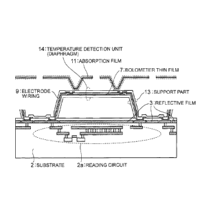
[0003] Fig. 14 is an explanatory diagram schematically illustrating a pixel
structure of
a two-dimensional bolometer-type THz-wave detector described in PTL 3. Fig. 14
illustrates a
sectional view of the two-dimensional bolometer-type THz-wave detector
[0004] Figs. 15, 16, and 17 are explanatory diagrams each schematically
illustrating a
pixel structure of the two-dimensional bolometer-type THz-wave detector
described in PTL 4.
Citation List
Patent Literature
[0005] PTL 1: Japanese Patent Application Laid-Open No. 2008-241438
PTL 2: Japanese Patent Application Laid-Open No. 2011-106825
PTL 3: Japanese Patent Application Laid-Open No. 2012-002603
PTL 4: Japanese Patent Application Laid-Open No. 2012-194080
Non Patent Literature
[0006] NPL 1: Oda et. al., Proceedings of SPIE, Vol. 6940,2008, pp. 69402Y-1
to
69402Y-12
Summary of Invention
[0007] A THz-wave detector is preferably able to detect THz waves with higher-
sensitivity. For example, the THz-wave detector described in PTL 3 detects THz
waves with
CA 2945597 2017-10-25
CA 02945597 2016-10-12
2
high sensitivity by using an interference between a reflective film 103 and an
absorption film 111
as illustrated in Fig. 14.
[0008] In the THz-wave detector as illustrated in Fig. 14, however, such a
phenomenon
that an output from the detector, in other words, THz sensor sensitivity
(hereinafter, simply
referred to as "sensor sensitivity") changes according to an angle between the
polarization
direction and the detector (polarization angle) is recognized when linear-
polarized THz waves
are incident on the detector. Specifically, in the THz-wave detector as
illustrated in Fig. 14, the
dependence of the sensor sensitivity on the polarization angle is recognized.
Fig. 18 is a graph
illustrating the dependence of the sensor sensitivity of the THz-wave detector
as illustrated in Fig.
14 on the polarization angle.
[0009] To achieve a higher-sensitivity THz-wave detector, it is necessary to
reduce the
dependence of the sensor sensitivity on the polarization angle.
[0010] Fig. 19 is a top view of a reflective film 103 of arrayed pixels (the
THz-wave
detector illustrated in Fig. 14). Fig. 19 illustrates the top view looking
down on the reflective
film 103 for a plurality of arrayed pixels. As illustrated in Fig. 19, in the
structure of the
reflective film 103 illustrated in Fig. 14, a gap is formed between pixels in
the reflective film 103.
THz waves pass through the gap between the pixels in the reflective film 103
and a substrate 102
(specifically, the metal wiring of the reading circuit 102a of the substrate
102) reflects or absorbs
the THz waves. Therefore, to study the THz reflection characteristics of the
THz-wave detector,
it is necessary to estimate the reflection/absorption in the metal wiring of
the reading circuit 102a,
It is, however, difficult to estimate the reflection/absorption in the metal
wiring of the reading
circuit 102a since the metal wiring of the reading circuit 102a normally
includes a plurality of
layers.
[0011] Fig. 20 illustrates the THz reflection characteristics of the THz-wave
detector in
which the structure on the upper side than the reflective film 103 is not
formed. Fig. 20 is a
graph illustrating the dependence of a reflectance on a polarization angle in
the case where the
structure on the upper side than the reflective film 103 of the THz-wave
detector illustrated in
Fig. 14 is not formed.
[0012] From the graph illustrated in Fig. 20, it is understood that the THz
reflectance
.. drastically changes according to the polarization angle. If the shape of
the gap in the reflective
film 103 is reflected on the THz reflection characteristics, the THz
reflection characteristics in
that case are supposed to show a four-fold symmetry in which a symmetry is
repeated every 90
degrees. It, however, can be estimated that reflection/absorption occurs from
the metal wiring
of the reading circuit 102a which is located in a lower part than the
reflective film 103 since the
81800422
3
THz reflection characteristics illustrated in Fig. 20 show a two-fold
symmetry. Specifically.
reflection/absorption in the metal wiring of the reading circuit 102a can be
estimated from the graph
illustrated in Fig. 20.
[0013] It is then found that there is a correlation between the dependence of
the sensor
sensitivity on the polarization angle and the dependence of the THz
reflectance of the substrate 102 on the
polarization angle from the graphs illustrated in Figs. 18 and 20.
Specifically, it is found that the sensor
sensitivity of the THz-wave detector is low in the polarization angle at which
the THz reflectance is low in
the substrate 102.
[0014] Therefore, it is an object of the present invention to provide a higher-
sensitivity
bolometer-type terahertz-wave detector capable of reducing the dependence of
the sensor sensitivity on the
polarization angle.
[0015] According to an aspect of the present invention, there is provided a
terahertz-wave
detector having a thermal separation structure in which a temperature
detection unit including a bolometer
thin film connected to electrode wiring is supported so as to be lifted above
a substrate by a support part
including the electrode wiring connected to a reading circuit formed on the
substrate, the terahertz-wave
detector comprising: a reflective film that is formed on the substrate and
reflects terahertz waves; and an
absorption film that is formed on the temperature detection unit and absorbs
terahertz waves, wherein the
reflective film is integrally formed with a reflective film of a terahertz-
wave detector adjacent to the
terahertz-wave detector to prevent terahertz waves from passing through a gap
in the reflective film.
[0016] According to another aspect of the present invention, there is provided
a terahertz-wave
detector having a thermal separation structure in which a temperature
detection unit including a bolometer
thin film connected to electrode wiring is supported so as to be lifted above
a substrate by a support part
including the electrode wiring connected to a reading circuit formed on the
substrate, the terahertz-wave
detector comprising: a second reflective film formed so as to cover a
reflective film on the upper side of the
reflective film that is formed on the substrate and reflects terahertz waves;
and an absorption film that is
formed on the temperature detection unit and absorbs terahertz waves, wherein
the second reflective film is
integrally formed with a second reflective film of a terahertz-wave detector
adjacent to the terahertz-wave
detector to prevent terahertz waves from passing through a gap in the second
reflective film.
[0017] According to another aspect of the present invention, there is provided
a terahertz-wave
detector having a thermal separation structure in which a temperature
detection unit including a bolometer
thin film connected to electrode wiring is supported so as to be lifted above
a substrate by a support part
including the electrode wiring connected to a reading circuit formed on the
substrate, the terahertz-wave
detector comprising: a reflective film that is formed on the substrate and
reflects terahertz waves; and an
absorption film that is formed on the temperature detection unit and absorbs
terahertz waves, wherein the
.. reflective film is formed without any space from a reflective film of a
terahertz-wave detector adjacent to
the terahertz-wave detector to prevent terahertz waves from passing through a
gap in the reflective film.
CA 2945597 2018-06-21
8.1800422
4
[0018] According to another aspect, there is provided a terahertz-wave
detector
having a thermal separation structure in which a temperature detection unit
including a
bolometer thin film connected to electrode wiring is supported so as to be
lifted above a substrate
by a support part including the electrode wiring connected to a reading
circuit formed on the
substrate, wherein the terahertz-wave detector is provided with a reflective
film that is formed on
the substrate and reflects terahertz waves and an absorption film that is
formed on the
temperature detection unit and absorbs terahertz waves and the reflective film
is formed so that
the dependence on the polarization angle is smaller than a predetermined
value.
[0019] Aspects of the present invention are able to reduce the dependence of
the
sensor sensitivity of the bolometer-type THz-wave detector on the polarization
angle and to
achieve higher-sensitivity THz wave detection.
Brief Description of Drawings
[0020]
[Fig. 1] Fig. 1 is an explanatory diagram schematically illustrating a pixel
structure
according to a first exemplary embodiment of a THz-wave detector according to
the present
invention.
[Fig. 2] Fig. 2 is a top view of a reflective film illustrated in Fig. 1.
[Fig. 3] Fig. 3 is a graph illustrating the dependence of a reflectance of a
THz-wave
detector illustrated in Fig. 1 on a polarization angle in the case where the
structure on the upper
side than the reflective film is not formed.
[Fig. 4] Fig. 4 is a graph illustrating the dependence of a reflectance of the
THz-wave
detector illustrated in Fig. 1 on a frequency in the case where the structure
on the upper side than
the reflective film is not formed.
[Fig. 5] Fig. 5 is a graph illustrating the dependence of sensor sensitivity
of the THz-
wave detector illustrated in Fig. 1 on the polarization angle.
[Fig. 6] Fig. 6 is a top view of an entire reflective film in the case where
the reflective
film is arranged between a contact and another contact
[Fig. 7] Fig. 7 is a top view of a reflective film in the case where a contact
is
electrically connected to a contact of another pixel.
[Fig. 8] Fig. 8 is an explanatory diagram schematically illustrating a pixel
structure of
CA 2945597 2018-06-21
81800422
a second exemplary embodiment of the THz-wave detector according to the
present invention.
[Fig. 9] Fig. 9 is a top view of a second reflective film illustrated in Fig.
8.
[Fig. 10] Fig. 10 is an explanatory diagram schematically illustrating a pixel
structure
of a third exemplary embodiment of the THz-wave detector according to the
present invention.
5 [Fig. 11] Fig. 11 is an explanatory diagram schematically illustrating a
pixel structure
of a fourth exemplary embodiment of the THz-wave detector according to the
present invention.
[Fig. 12] Fig. 12 is an explanatory diagram schematically illustrating a pixel
structure
of a fifth exemplary embodiment of the THz-wave detector according to the
present invention.
[Fig. 13] Fig. 13 is an explanatory diagram illustrating the minimum
configuration of
the terahertz-wave detector according to an embodiment of the present
invention.
[Fig. 14] Fig. 14 is an explanatory diagram schematically illustrating a pixel
structure
of a two-dimensional bolometer-type THz-wave detector described in PTL 3.
[Fig. 15] Fig. 15 is an explanatory diagram schematically illustrating a pixel
structure
of a two-dimensional bolometer-type THz-wave detector described in PTL 4.
[Fig. 16] Fig. 16 is an explanatory diagram schematically illustrating a pixel
structure
of the two-dimensional bolometer-type THz-wave detector described in PTL 4.
[Fig. 171 Fig. 17 is an explanatory diagram schematically illustrating a pixel
structure
of the two-dimensional bolometer-type THz-wave detector described in PTL 4.
[Fig. 18] Fig. 18 is a graph illustrating the dependence of sensor sensitivity
of the THz-
wave detector illustrated in Fig. 14 on a polarization angle.
[Fig. 19] Fig. 19 is a top view of a reflective film of arrayed pixels (the
THz-wave
detector illustrated in Fig. 14).
[Fig. 20] Fig. 20 is a graph illustrating the dependence of a reflectance of
the THz-
wave detector illustrated in Fig. 14 on the polarization angle in the case
where the structure on
the upper side than the reflective film is not formed.
[Fig. 21] Fig. 21 is a graph illustrating the dependence of the reflectance of
the THz-
wave detector illustrated in Fig. 14 on the frequency in the case where the
structure on the upper
side than the reflective film is not formed.
Description of Embodiment
Exemplary Embodiment 1
[0021] Hereinafter, a first exemplary embodiment of the present invention will
be
described with reference to drawings.
[0022] Fig. 1 is an explanatory diagram schematically illustrating a pixel
structure
according to a first exemplary embodiment of a THz-wave detector according to
the present
CA 2945597 2017-10-25
CA 02945597 2016-10-12
=
6
invention. In Fig. 1, a sectional view of the THz-wave detector is
illustrated.
[0023] As illustrated in Fig. 1, the THz-wave detector includes a reading
circuit 2a, a
substrate 2, a reflective film 3, a contact 4, a first protective film 5,
electrode wiring 9, an eave-
like member 12, a support part 13, and a temperature detection unit
(diaphragm) 14.
[0024] The substrate 2, the reading circuit 2a, the reflective film 3, the
contact 4, the
first protective film 5, the electrode wiring 9, the cave-like member 12, the
support part 13, and
the temperature detection unit 14 are the same as a substrate 102, a reading
circuit 102a, a
reflective film 103, a contact 104, a first protective film 105, electrode
wiring 109, an cave-like
member 112, a support part 113, and a temperature detection unit 114, and
therefore the
description thereof is omitted here.
[0025] Moreover, a second protective film 6, a third protective film 8, and a
fourth
protective film 10 included by the support part 13 are the same as a second
protective film 106, a
third protective film 108, and a fourth protective film 110 included by the
support part 113
illustrated in Fig. 14, and therefore the description thereof is omitted here.
Furthermore, a
bolometer thin film 7 and an absorption film 11 included by the temperature
detection unit 14 are
the same as a bolometer thin film 107 and an absorption film 111 included by
the temperature
detection unit 114 illustrated in Fig. 14, and therefore the description
thereof is omitted here.
[0026] In this exemplary embodiment, as illustrated in Fig. 1, the reflective
film 3 is
formed so as to be integrated with an adjacent reflective film to prevent a
gap from being formed
between pixels adjacent to each other in the reflective film 3. Fig. 2 is a
top view of the
reflective film 3 illustrated in Fig. 1. Fig. 2 illustrates a top view looking
down on the reflective
film 3 for a plurality of arrayed pixels. In this manner, the reflective film
3 is arranged without
a gap to prevent THz waves from passing through the gap so as to inhibit an
occurrence of
reflection or absorption from or into the metal wiring of the reading circuit
2a in this exemplary
embodiment. This enables a reduction in the dependence of the THz reflectance
of the
substrate 2 on the polarization angle. Although the reflective film is
integrally formed in this
exemplary embodiment, the reflective film does not always need to be
integrally formed, but the
reflective film 3 may be foinied separately as long as the gap is not formed.
[0027] The following describes THz reflection characteristics of the THz-wave
detector according to the present invention.
[0028] For facilitating the description of the advantageous effects of the
present
invention, the reflective film 3 is formed as illustrated in Fig. 1 and Figs.
3 and 4 illustrate the
THz reflection characteristics of the THz-wave detector in which the structure
on the upper side
than the reflective film 3 is not formed. Fig. 3 is a graph illustrating the
dependence of a
CA 02945597 2016-10-12
7
reflectance of the THz-wave detector illustrated in Fig. 1 on a polarization
angle in the case
where the structure on the upper side than the reflective film 3 is not
formed.
[0029] In the graph illustrated in Fig. 3, any dependence of the THz
reflectance on the
polarization angle as in the graph illustrated in Fig. 20 is not found.
[0030] Furthermore, Fig. 5 illustrates the dependence of the sensor
sensitivity of the
THz-wave detector of this exemplary embodiment on the polarization angle. In
the graph
illustrated in Fig. 5, any dependence of the sensor sensitivity on the
polarization angle as in Fig.
18 is not found, and thus an advantageous effect of the present invention is
obvious.
[0031] Fig. 4 is a graph illustrating the dependence of a reflectance of the
THz-wave
detector illustrated in Fig. 1 on a frequency in the case where the structure
on the upper side than
the reflective film 3 is not formed. Fig. 4 illustrates the dependence of the
THz reflectance on
the frequency at the polarization angles of 0, 120, and 240 degrees. Fig. 21
is a graph
illustrating the dependence of the reflectance of the THz-wave detector
illustrated in Fig. 14 on
the frequency in the case where the structure on the upper side than the
reflective film 3 is not
formed. In the graph illustrated in Fig. 4, any large fluctuation of the THz
reflectance caused
by the frequency and the polarization angle as illustrated in Fig. 21 is not
found. In other words,
the THz-wave detector of this exemplary embodiment is able to reduce the
variation of the
dependence of the THz reflectance on the polarization angle caused by
frequency and is able to
maintain the dependence of the sensor sensitivity on the polarization angle to
be low even if the
frequency changes.
[0032] Incidentally, it is found by the study of the present inventor that the
advantageous effect of the present invention is more obvious in the case where
the sheet
resistance of the reflective film 3 is 100 n/sq or less.
[0033] As described hereinabove, the reflective film 3 is formed to prevent a
gap from
being formed between pixels in the reflective film 3 in the exemplary
embodiment. This
prevents THz waves from passing through the gap in the reflective film 3,
thereby enabling a
reduction in the dependence of the THz reflectance of the substrate 2 on the
polarization angle.
This makes it more difficult for such a phenomenon that an output (sensor
sensitivity) from the
THz-wave detector changes according to the polarization angle to occur.
Specifically, the
present invention is able to reduce the dependence of the sensor sensitivity
on the polarization
angle in the THz-wave detector for detecting THz waves by using an
interference between the
reflective film and the absorption film as illustrated in Fig. 14.
[0034] If the area of the contact 4 illustrated in Fig. 2 is not so large, the
reflective film
3 may be arranged between the contact 4 and a contact of another pixel. In
that case, the
CA 02945597 2016-10-12
8
reflective film 3 is formed as illustrated in Fig. 6. Fig. 6 is a top view of
the entire reflective
film 3 in the case where the reflective film 3 is arranged between the contact
4 and a contact of
another pixel. Fig. 6 illustrates the top view looking down on the reflective
film 3 for a
plurality of arrayed pixels. The formation of the reflective film 3 as in Fig.
6 enables the area
of the reflective film 3 to increase as far as possible, thereby enabling a
further reduction in the
dependence of the sensor sensitivity of the THz-wave detector on the
polarization angle.
[0035] Moreover, one of the contacts 4 of the THz-wave detector may be
electrically
connected to a contact 4 of another THz-wave detector. In that case, as
illustrated in Fig. 7, the
gap between the reflective film 3 and the contact 4 (a hole for the contact 4
formed in the
reflective film 3), which is provided in the reflective film 3, can be
reduced. Thereby, the area
of the reflective film 3 is able to be increased as far as possible, thereby
enabling the dependence
of the sensor sensitivity of the TIz-wave detector on the polarization angle
to be further reduced.
Fig. 7 is a top view of the reflective film 3 in the case where the contact 4
is electrically
connected to a contact of another pixel. Fig. 7 illustrates a top view looking
down on the
reflective film 3 for a plurality of arrayed pixels.
Exemplary Embodiment 2
[0036] Hereinafter, a second exemplary embodiment will be described with
reference
to drawings.
[0037] Fig. 8 is an explanatory diagram schematically illustrating a pixel
structure of
the second exemplary embodiment of the THz-wave detector according to the
present invention.
Fig. 8 illustrates a sectional view of the THz-wave detector.
[0038] The pixel structure of the second exemplary embodiment is the same as
the
pixel structure of the first exemplary embodiment. As illustrated in Fig. 8,
however, the THz-
wave detector in this exemplary embodiment includes a second reflective film
3a in addition to
the constituent elements illustrated in Fig. 1. Fig. 9 is a top view of the
second reflective film
3a illustrated in Fig. 8. Fig. 9 illustrates a top view looking down on the
second reflective film
3a for a plurality of arrayed pixels.
[0039] In this exemplary embodiment, the second reflective film 3a is formed
so as to
cover the reflective film 3 as illustrated in Figs. 8 and 9. The reflective
film 3 and the second
reflective film 3a are physically separated from each other. In addition, the
second reflective
film 3a and the absorption film 11 form an optical resonance structure.
[0040] This exemplary embodiment is effective in the case where the reflective
film 3
cannot be connected to a reflective film of an adjacent pixel according to
convenience for
manufacturing the THz sensor. For example, in the case where a voltage is
applied to the
CA 02945597 2016-10-12
9
reflective film 3, short-circuiting is likely to occur when the reflective
film 3 is connected to a
reflective film of an adjacent pixel. In that case, the second reflective film
3a physically
separated from the reflective film 3 is formed so as to cover the reflective
film 3, thereby
achieving an equivalent advantageous effect to the first exemplary embodiment.
[0041] Furthermore, similarly to the first exemplary embodiment, it is found
by the
study of the present inventor that the advantageous effect of the present
invention is more
obvious if the sheet resistance of the second reflective film 3a is 100 Q/sq
or less.
Exemplary Embodiment 3
[0042] Hereinafter, a third exemplary embodiment of the present invention will
be
described with reference to drawings.
[0043] Fig. 10 is an explanatory diagram schematically illustrating a pixel
structure of
the third exemplary embodiment of the TIIz-wave detector according to the
present invention.
Fig. 10 illustrates a sectional view of the THz-wave detector.
[0044] The pixel structure of the third exemplary embodiment is the same as
the pixel
.. structure of the first exemplary embodiment.
[0045] In this exemplary embodiment, however, the THz-wave detector does not
include the eave-like member 12. Moreover, in this exemplary embodiment, the
film thickness
of the first protective film 5 is set so that a gap (air gap 16) between the
upper surface of the first
protective film 5 and the lower surface of the temperature detection unit 14
is less than 8 pin
without a change in the gap (gap 15) between the reflective film 3 and the
absorption film 11.
[0046] Specifically, this exemplary embodiment is obtained by applying the
reflective
film 3 of the first exemplary embodiment to the THz-wave detector illustrated
in Fig. 15. In
this manner, the present invention may be applied to the THz-wave detector
illustrated in Fig. 15.
Thereby, an equivalent advantageous effect to the first exemplary embodiment
is achieved also
in the THz-wave detector as illustrated in Fig. 15.
[0047] In addition, the second reflective film 3a of the second exemplary
embodiment
may be applied to the THz-wave detector illustrated in Fig. 15. Thereby, in
the THz-wave
detector as illustrated in Fig. 15, an equivalent advantageous effect to the
first exemplary
embodiment is achieved even if the reflective film 3 cannot be connected to a
reflective film of
an adjacent pixel according to convenience for manufacturing the THz sensor.
Exemplary Embodiment 4
[0048] Hereinafter, a fourth exemplary embodiment of the present invention
will be
described with reference to drawings.
[0049] Fig. 11 is an explanatory diagram schematically illustrating a pixel
structure of
CA 02945597 2016-10-12
the fourth exemplary embodiment of the THz-wave detector according to the
present invention.
Fig. 11 illustrates a sectional view of the THz-wave detector.
[0050] The pixel structure of the fourth exemplary embodiment is the same as
the pixel
structure of the third exemplary embodiment. In this exemplary embodiment,
however, the
5 .. cave-like member 12 is formed over the temperature detection unit 14.
[0051] Specifically, this exemplary embodiment is obtained by applying the
reflective
film 3 of the first exemplary embodiment to the THz-wave detector illustrated
in Fig. 16. In
this manner, the present invention may be applied to the THz-wave detector
illustrated in Fig. 16.
Thereby, an equivalent advantageous effect to the first exemplary embodiment
is achieved also
10 in the THz-wave detector as illustrated in Fig. 16.
[0052] In addition, the second reflective film 3a of the second exemplary
embodiment
may be applied to the THz-wave detector illustrated in Fig. 16. Thereby, in
the THz-wave
detector as illustrated in Fig. 16, an equivalent advantageous effect to the
first exemplary
embodiment is achieved even if the reflective film 3 cannot be connected to a
reflective film of
an adjacent pixel according to convenience for manufacturing the THz sensor.
Exemplary Embodiment 5
[0053] Hereinafter, a fifth exemplary embodiment of the present invention will
be
described with reference to drawings.
[0054] Fig. 12 is an explanatory diagram schematically illustrating a pixel
structure of
the fifth exemplary embodiment of the THz-wave detector according to the
present invention.
Fig. 12 illustrates a sectional view of the THz-wave detector.
[0055] The pixel structure of the fifth exemplary embodiment is the same as
the pixel
structure of the second exemplary embodiment.
[0056] In this exemplary embodiment, however, a multilayer wiring structure
for
connecting the electrode wiring 9 to the reading circuit 2a is formed by
sequentially laminating a
via and a wiring layer on the wiring used as the reflective film 3 by using a
wiring fonning
method in a semiconductor manufacturing process. Thereby, breakage of the
electrode wiring 9
can be suppressed. The interlayer dielectric film 21 is a dielectric film
between laminated
wiring layers.
[0057] Specifically, this exemplary embodiment is obtained by applying the
second
reflective film 3a of the second exemplary embodiment to the THz-wave detector
illustrated in
Fig. 17. In this manner, the present invention may be applied to the THz-wave
detector
illustrated in Fig. 17. Thereby, an equivalent advantageous effect to the
first exemplary
embodiment is achieved even if the reflective film 3 is not able to be
connected to the reflective
CA 02945597 2016-10-12
11
film of an adjacent pixel according to convenience for manufacturing the THz
sensor in the THz-
wave detector as illustrated in Fig. 17.
[0058] Incidentally, the reflective film 3 of the first exemplary embodiment
may be
applied to the THz-wave detector illustrated in Fig. 17. Specifically, the THz-
wave detector
.. illustrated in Fig. 17 may include the reflective film 3 instead of the
reflective film 103. Also in
that exemplary embodiment, an equivalent advantageous effect to the first
exemplary
embodiment is achieved.
[0059] Subsequently, the outline of the present invention will be described.
Fig. 13 is
an explanatory diagram illustrating the minimum configuration of the terahertz-
wave detector
.. according to the present invention. The terahertz-wave detector according
to the present
invention is a terahertz-wave detector having a thermal separation structure
in which a
temperature detection unit 14 including a bolometer thin film 7 connected to
electrode wiring 9
is supported so as to be lifted above a substrate 2 by a support part 13
including the electrode
wiring 9 connected to a reading circuit 2a formed on the substrate 2, wherein
the terahertz-wave
detector is provided with a reflective film 3 that is formed on the substrate
2 and reflects
terahertz waves and an absorption film 11 that is fonned on the temperature
detection unit 14 and
absorbs terahertz waves and the reflective film 3 is integrally formed with
the reflective film of
an adjacent terahertz-wave detector.
[0060] According to the above configuration, the present invention is able to
prevent
THz waves from passing through a gap in the reflective film 3 and to reduce
the dependence of
the THz reflectance of the substrate 2 on the polarization angle. This makes
it more difficult for
such a phenomenon that an output (sensor sensitivity) from the detector
changes according to the
polarization angle to occur. Specifically, the present invention is able to
reduce the dependence
of the sensor sensitivity on the polarization angle in the THz-wave detector
for detecting THz
waves by using an interference between the reflective film and the absorption
film as illustrated
in Fig. 14.
[0061] Moreover, the sheet resistance of the reflective film 3 may be 100
C2/sq or less.
This configuration enables the dependence of the sensor sensitivity of the THz-
wave detector on
the polarization angle to be further reduced.
[0062] Furthermore, a hole for a contact 4 may be formed in the reflective
film 3
according to the area of the contact 4 electrically connecting the reading
circuit 2a formed on the
substrate 2 to the electrode wiring 9 included by the support part 13. This
configuration enables
the area of the reflective film 3 to be increased as far as possible and thus
enables the
dependence of the sensor sensitivity of the THz-wave detector on the
polarization angle to be
CA 02945597 2016-10-12
12
further reduced.
[0063] Moreover, the terahertz-wave detector according to the present
invention is a
terahertz-wave detector having a thermal separation structure in which a
temperature detection
unit 14 including a bolometer thin film 7 connected to electrode wiring 9 is
supported so as to be
lifted above a substrate 2 by a support part 13 including the electrode wiring
9 connected to a
reading circuit 2a formed on the substrate 2, wherein the terahertz-wave
detector is provided
with a second reflective film 3a formed so as to cover a reflective film 3 on
the upper side of the
reflective film 3 that is formed on the substrate 2 and reflects terahertz
waves and an absorption
film 11 that is formed on the temperature detection unit 14 and absorbs
terahertz waves and the
second reflective film 3a is integrally formed with the second reflective film
of an adjacent
terahertz-wave detector.
[0064] If the second reflective film 3a that covers the reflective film 3 is
integrally
formed with the second reflective film of the adjacent pixel instead of
integrally forming the
reflective film 3 with the reflective film of the adjacent pixel in this
manner, the dependence of
the sensor sensitivity of the THz-wave detector on the polarization angle can
be reduced even in
the case where the reflective film 3 cannot be connected to the reflective
film of the adjacent
pixel according to convenience for manufacturing the THz sensor.
[0065] Moreover, the reflective film 3 and the second reflective film 3a may
be
separated from each other. For example, in the case where a voltage is applied
to the reflective
film 3, short-circuiting is likely to occur when the reflective film 3 is
connected to the reflective
film of the adjacent pixel. In that case, according to the aforementioned
configuration, the
reflective film 3 and the second reflective film 3a are physically separated
from each other,
thereby enabling a reduction in the dependence of the sensor sensitivity of
the THz-wave
detector on the polarization angle.
[0066] Furthemiore, the sheet resistance of the second reflective film 3a may
be 100
Q/sq or less. This configuration enables the dependence of the sensor
sensitivity of the THz-
wave detector on the polarization angle to be further reduced.
[0067] Furthermore, the terahertz-wave detector according to the present
invention is a
terahertz-wave detector having a thermal separation structure in which a
temperature detection
unit 14 including a bolometer thin film 7 connected to electrode wiring 9 is
supported so as to be
lifted above a substrate 2 by a support part 13 including the electrode wiring
9 connected to a
reading circuit 2a formed on the substrate 2, wherein the terahertz-wave
detector is provided
with a reflective film 3 that is formed on the substrate 2 and reflects
terahertz waves and an
absorption film 11 that is formed on the temperature detection unit 14 and
absorbs terahertz
81800422
13
waves and the reflective film 3 is formed without any space from the
reflective film of an
adjacent terahertz-wave detector.
[0068] According to the configuration, THz waves can be prevented from passing
through the gap in the reflective film 3 even in the case where the reflective
film is separated
from the reflective film of the adjacent terahertz-wave detector and not
integrally formed with
the reflective film thereof. This enables a reduction in the dependence of the
THz reflectance
of the substrate 2 on the polarization angle.
[0069] Moreover, the terahertz-wave detector according to the present
invention is a
terahertz-wave detector having a thermal separation structure in which a
temperature detection
unit 14 including a bolometer thin film 7 connected to electrode wiring 9 is
supported so as to be
lifted above a substrate 2 by a support part 13 including the electrode wiring
9 connected to a
reading circuit 2a formed on the substrate 2, wherein the terahertz-wave
detector is provided
with a reflective film 3 that is formed on the substrate 2 and reflects
terahertz waves and an
absorption film 11 that is formed on the temperature detection unit 14 and
absorbs terahertz
waves and the reflective film 3 is formed so that the dependence of the
terahertz-wave
reflectance on the polarization angle is smaller than a predetermined value.
[0070] This configuration makes it more difficult for such a phenomenon that
an
output (sensor sensitivity) from the THz-wave detector changes according to
the polarization
angle to occur.
[0071] Although the present invention has been described with reference to the
exemplary embodiments and examples hereinabove, the present invention is not
limited thereto.
A variety of changes, which can be understood by those skilled in the art, may
be made in the
configuration and details of the present invention within the scope thereof.
[0072]
Reference Signs List
[0073]
2, 102 Substrate
2a, 102a Reading circuit
3, 103 Reflective film
3a Second reflective film
4, 104 Contact
5, 105 First protective film
CA 2945597 2017-10-25
CA 02945597 2016-10-12
14
6, 106 Second protective film
7, 107 Bolometer thin film
8, 108 Third protective film
9, 109 Electrode wiring
10, 110 Fourth protective film
11, 111 Absorption film
12, 112 Eave-like member
13, 113 Support part
14, 114 Temperature detection unit (diaphragm)
15, 115 Gap
16,116 Air gap