Note: Descriptions are shown in the official language in which they were submitted.
CA 02945623 2016-10-13
Description
Device and method for transmitting differential data
signals
The invention relates to an apparatus and a method for
signal transmission for differential data signals on a
high speed data link and particularly for reducing a
common mode signal component. The apparatus comprises a
printed circuit board having a conductor pair having a
first signal conductor and a second signal conductor
for transmitting the differential data signal.
In the realm of data transmission, for example in
computer networks, data transmission involves the use
of data cables that typically have multiple data lines
combined in a common cable sheath. For high speed data
transmissions, the data lines used in each case are
shielded wire pairs, the two wires particularly running
parallel to one another or alternatively being twisted
together. In this case, a respective wire consists of
the actual conductor, for example a solid conductor
wire or a stranded conductor, each of which is
surrounded by an insulation. The wire pair of a
respective data line is surrounded by a (pair) shield.
The data cables typically have a multiplicity of wire
pairs shielded in this manner that are surrounded by a
common cable sheath. Such data cables are used for high
speed data links and are designed for data rates of
greater than 5 Gbit/s.
Such data cables are connected to connectors in a pre-
assembled manner. In the case of applications for high
speed transmissions, the connectors are then frequently
in the form of what are known as small form pluggable
connectors, SFP connectors for short. There are
different variant embodiments of these, for example
what are known as SFP-, SFP+, QSFP- or CXP- connectors.
These connectors have special connector housings, as
can be seen from WO 2011 072869 Al or
CA 02945623 2016-10-13
- 2 -
WO 2011 089003 Al, for example.
Inside, such connector housings have a printed circuit
board or card in part with integrated electronics. On
this card, the respective data cable can be connected
using a connector reverse. This involves the individual
wires of the data cable being soldered or welded to the
card. At the opposite end of the card, said end
typically forms a plug-in tongue with connection
contacts that are inserted into a mating connector.
Such cards are also referred to as paddle cards.
In this case, the pair shielding of a respective wire
pair is - as can be seen from EP 2 112 669 A2, for
example - in the form of a longitudinally folded foil
shield. The shield is therefore folded around the wire
pair so as to run in a longitudinal direction of the
cable, the two ends overlapping in an overlap region
that runs in the longitudinal direction. The shielding
foil used for the shield is a multilayer shield
comprising at least one conductive (metal) layer and an
insulating layer. The conductive layer used is usually
an aluminum layer, and the insulating layer used is a
PET film. The PET film is in the form of a support on
which a metal coating has been applied to form the
conductive layer.
Besides the longitudinally folded shielding for pairs
with parallel routing, there is fundamentally also the
possibility of wrapping such a shielding foil helically
around the wire pair. However, at higher signal
frequencies upward of approximately 15 GHz, such
braiding of the wire pair with a shielding foil is not
readily possible on account of resonance effects. At
these high frequencies, the shielding foil is therefore
added as a longitudinally folded foil.
Such a longitudinally folded foil is accompanied by an
undesirable negative side effect, however. What is
CA 02945623 2016-10-13
- 3 -
known as the common mode signal is no longer attenuated
to a sufficient degree with the longitudinally folded
shields, as is the case with braiding with a shielding
foil.
Such data cables are typically what are known as
balanced data lines, which are designed for
differential data transmission. This involves the two
wires being used to transmit the same signal in
inverted form. The differential signal component
between these two signals is evaluated, so that
external effects, which affect both signals, are
eliminated.
The formation of the common mode signal in the case of
such balanced lines with parallel pairs is known in
principle. Attenuation of this undesirable common mode
signal is additionally hampered by the fact that this
common mode signal component propagates more quickly
than the differential signal component that is actually
of interest. The absent or severely reduced attenuation
of this common mode signal in comparison with braided
wire pairs therefore leads to impairment of what is
known as the skew or what is known as the mode
conversion performance.
With such high speed data links, an increase in
transmission power is generally sought. The
transmission rates and hence the frequency range of
such data cables therefore increase to an ever greater
extent, and hence so do the problems relating to the
common mode signal components.
In order to filter out common mode signal components,
US 2011/0273245 Al, for example, discloses the practice
of introducing a meandrous structure in a ground plane
of a multilayer printed circuit board.
The article "Miniaturization of Common Mode Filter
CA 02945623 2016-10-13
- 4 -
based on EBG Patch Resonance", Francesco De Paulis et
al, DesignCon 2012 "Where Chipheads Connect", Santa
Clara, California, USA, January 30 - February 02, 2012,
Proceedings, pages 2320-2338, describes a common mode
filter in which a multilayer printed circuit board has,
arranged beneath a conductor track, a matrix-shaped
conductive structure, what is known as the EBG plane,
between the conductor track and a ground plane.
Finally, US 2004/0119553 Al discloses the practice of
avoiding spurious signals caused by a common mode
signal by electrically connecting the two signal
conductors to ground via a resistor and a capacitance.
Against this background, the invention is based on the
object of allowing such a high speed data link to have
improved data transmission at high signal frequencies
of greater than 10 GHz and of achieving a high level of
attenuation for a common mode signal.
The object is achieved in accordance with the invention
by means of an apparatus having the features of claim 1
and by means of a method having the features of claim
16. Preferred developments are contained in the
subclaims. The preferred embodiments cited for the
apparatus can also be transferred mutatis mutandis to
the method.
The apparatus is designed particularly for transmitting
data signals in a high speed data link at a
transmission rate of typically greater than 10 Gbit per
second. It has a printed circuit board having a
conductor pair added thereto having a first signal
conductor and a second signal conductor, which are used
to transmit a differential data signal during
operation. Additionally, the conductor pair has an
associated decoupling line that runs symmetrically and
without interruption in relation to the signal
conductors and into which common mode signal components
CA 02945623 2016-10-13
- 5 -
are decoupled during operation. Additionally, the
decoupling line is connected to a ground conductor,
that is to say to ground potential, via at least one
attenuating element.
This embodiment selectively decouples only the common
mode signal components from the signal conductors into
the decoupling line, where they are attenuated by the
attenuating element. The attenuating element therefore
consumes the energy in the common mode signal
component, and the undesirable common mode signal
components are absorbed at least in part.
This embodiment is based on the consideration that
selective decoupling of the common mode signal
components is possible for a differential signal
transmission. Decoupling the spurious common mode
signal components therefore allows them to be
effectively reduced, in particular attenuated. The
spurious signal component is therefore at least reduced
by means of decoupling from the transmission path.
The functional principle of the decoupling line is
based on the differential components in total
decoupling no power into the decoupling line, since -
owing to the symmetrical arrangement of the decoupling
line - their signal components are subtracted from one
another in each case. Conversely, especially in the
case of the common mode signals, the components on the
two signal conductors are added, which means that they
are thus coupled into the decoupling line by means of
coupling mechanisms.
The functional principle of the apparatus is therefore
designed in the manner of a directional coupler, in
which particular signal components, in this case the
common mode signal components, within a particular
frequency band are thus decoupled from the transmission
path.
CA 02945623 2016-10-13
- 6 -
In this case, the decoupling line extends over a
coupling path without interruption and symmetrically in
relation to the signal conductors. In this context,
without interruption is understood to mean that the
decoupling line forms a continuous conductive path,
particularly a continuous conductor track. In this
case, the two signal conductors have particularly
precisely one associated decoupling line that runs
symmetrically in relation to the signal conductors. The
signal conductors themselves run parallel to one
another at least over large sections.
In this context, symmetrical arrangement of the
decoupling line is understood to mean that the
decoupling line, at least over a large portion of its
length, is at the identical same distance - in a
transverse plane perpendicular to the direction of
propagation of the signal conductors - from each of the
signal conductors. In other words: The signal
conductors are situated within a common conductor
plane. They have a (mirror) symmetrical arrangement in
respect of a center plane that is oriented
perpendicular to the conductor plane. In addition, the
decoupling line is in (mirror) symmetrical form in
respect of this center plane. This symmetrical
arrangement fundamentally ensures that only the common
mode signal components, and not also differential
signal components, for example, are decoupled. In this
case, this symmetrical arrangement preferably extends
over the entire decoupling line, so that the decoupling
line is at the same distance from the two signal
conductors at each longitudinal position. To a certain
extent, the decoupling line therefore forms an axis of
symmetry for the entire decoupling structure.
To maintain the symmetry in the region of the
attenuating element too, an expedient embodiment - at
least as seen in a projection or in plan view - has
CA 02945623 2016-10-13
- 7 -
said attenuating element arranged symmetrically between
the signal conductors. On account of the installation
space required for the electronic assembly for the
attenuating element and the usually comparatively
narrow parallel course of the signal conductors, a
preferred development additionally has provision for a
distance of the signal conductors from one another to
be increased in the region of the attenuating element.
To this end, the two signal conductors flare in an
approximately funnel-like manner in a transition region
and subsequently run parallel to one another at an
increased distance in the region of the attenuating
element. This interspace at the increased distance then
contains the attenuating element in a symmetrical
arrangement between the signal conductors.
Differential signal lines of this kind frequently have
an electronic component, particularly what is known as
an isolating capacitor (DC isolating capacitor),
connected to the respective signal conductor. In this
case too, again in view of the desired symmetry, a
preferred embodiment has provision for the distance of
the signal conductors from one another to be increased
in the region of such components. At the same time or
alternatively, the decoupling line has a taper in the
style of a constriction in the region of such
components. In particular, an increase in the distance
between the signal conductors is combined with a taper
in the decoupling line. Overall, this measure allows a
compact, space-saving arrangement of such components on
the printed circuit board while maintaining the desired
symmetry.
Expediently, the printed circuit board comprises
multiple layers, at least one of which is in the form
of a ground layer having the ground conductor. The
attenuating element is expediently connected to this
ground layer, that is to say to the ground conductor,
via what is known as a plated-through hole through
CA 02945623 2016-10-13
- 8 -
multiple layers to the ground conductor. In this case,
a respective layer of the printed circuit board is
formed by an insulating support layer made of substrate
material having electrical layers or electrical
conductor tracks added thereto. The substrate material
is a standard substrate material for printed circuit
boards. The plated-through holes therefore form
electrically conductive connections between the
attenuating element and the ground conductor. Such
plated-through holes are likewise known in principle in
printed circuit board technology. In this regard, by
way of example, perpendicular holes penetrating the
substrate material are made whose inner wall is
conductive, so that a conductive connection is formed
through the substrate material.
In an expedient form, ground regions are formed at the
edge in a respective layer, so that the signal
conductors and/or the decoupling line are thus arranged
between ground potentials within the respective plane.
In this case, the edge ground regions are again formed
by preferably extensive conductor track regions. These
are connected to the ground plane by preferably a
multiplicity of plated-through holes extending along
the conductor tracks.
In a preferred development, the attenuating element is
connected to the decoupling line at an outer region
thereof. In this case, the electrically conductive
connection to the ground conductor is made at an inward
distance, that is to say at a distance from the
outermost region of the decoupling line. For the
connection to the ground conductor, an aperture is
formed in the decoupling line, the plated-through hole
being arranged in this aperture. This measure allows
the length of the decoupling line to be maximized for a
given total length of the printed circuit board. At the
same time, the aperture in the decoupling line
continues to maintain the desired symmetry. The
CA 02945623 2016-10-13
- 9 -
aperture is therefore a symmetrical recess in the
decoupling line that is at the same distance from the
two signal conductors. The recess is circular, in
particular, in this case.
In an expedient embodiment, an attenuating element is
expediently arranged at each end of the decoupling line
and connected to the ground conductor. This achieves
effective attenuation of the common mode signal
component.
The attenuating element is additionally preferably a
nonreactive resistance. For a typical application, the
resistance value in this case is in the region of a few
ohms, for example in the range from 5 to 50 ohms and
particularly approximately in the region of 20 ohms per
attenuating element.
In principle, there is the possibility of arranging the
decoupling line and the signal conductors next to one
another within one layer. However, studies have shown
that this achieves only limited attenuation of the
common mode signal components.
In an expedient development, there is therefore
provision for the decoupling line and the signal
conductors to be arranged in different layers.
Preferably, the signal conductors are arranged within
one layer in this case. The decoupling line is formed,
in a manner isolated by a substrate material of the
printed circuit board, in a layer particularly beneath
the two signal conductors. In this case, the plane of
the decoupling line is arranged preferably at a
distance of from 80 um to 200 pm and particularly at a
distance of approximately 100 pm from the plane of the
signal conductors. That is to say that the thickness of
the substrate between the signal conductors and the
decoupling line corresponds to this distance.
CA 02945623 2016-10-13
- 10 -
At the same time, a substrate thickness of a further
printed circuit board layer between decoupling line and
ground conductor is preferably different therefrom,
particularly greater, and is particularly in a range
between 200 pm and 400 pm and particularly in the
region of approximately 300 pm. The individual
substrate or support layers of the multilayer printed
circuit board are chosen in accordance with the
respective electrical and/or mechanical demands. The
choice of a comparatively thin substrate layer between
the signal conductors and the decoupling line achieves
efficient decoupling of the undesirable common mode
signal components. The substrate materials between the
signal conductors and the decoupling line additionally
preferably has a dielectric constant of approximately
3.4. Overall, this design achieves good decoupling.
Expediently, the decoupling line extends over the two
signal conductors in a transverse direction, so that
the decoupling line is distinctly wider in comparison
with the signal conductors. Generally, the signal
conductors and also the decoupling line are in the form
of flat conductor tracks of the card. Such conductor
tracks are produced in a manner that is known per se.
Preferably, the decoupling line - as seen in a
projection - terminates laterally at the outer edge of
the two signal conductors, i.e. the width of the
decoupling line corresponds to a distance between the
outer edges of the signal conductors.
Preferably, the signal conductors do not extend
linearly, and therefore run, at least in subregions,
obliquely in relation to a printed circuit board
longitudinal direction too. This measure achieves
particularly adjustment and particularly increase of
the conductor length on the printed circuit board. The
adjustment of the length likewise also achieves the
adjustment of a length of the coupling line and hence
of the coupling path. The length of the coupling path
affects the frequency band of the common mode signal
CA 02945623 2016-10-13
- 11 -
component, which is decoupled and attenuated.
In an expedient embodiment, there is therefore also
provision for the length of the coupling line to be
chosen on the basis of a prescribed frequency band
within which the undesirable common mode signals are
decoupled. Preferably, the length is then chosen
particularly such that there is an at least local
attenuation maximum for the common mode signal in the
range between 1 and 5 GHz and particularly at
approximately 3 GHz. For the purpose for high speed
data transmissions that is under consideration in the
present case, the length of the coupling line is in a
range between 10 and 18 and particularly in a range
between 12 and 15 mm, for example, for data rates
> 5 Gbit/sec. Overall, the length of the coupling line
is thus geared to the frequency band for which the
decoupling in the manner of a filter is intended to
take place (frequency band within which there is an
absorption maximum). The greater the frequency, the
shorter the coupling length is chosen (vice versa
proportionally).
The printed circuit board usually has a rear connection
region for a data cable having at least one signal
pair, preferably having multiple signal pairs. In the
front region, said printed circuit board is preferably
in the form of a plug-in tongue of the connector and
has contact strips. The decoupling structure and the
decoupling line extend - except for these edge
connection or contact regions - preferably over the
entire available length of the printed circuit board,
that is to say over a central region between the edge
connection and contact regions. In this case, these
connection and contact regions are formed particularly
by contact pads, usually widened end conductor track
regions. In addition, special coatings may be provided.
To make contact with the attenuating element on the
CA 02945623 2016-10-13
- 12 -
decoupling line, the latter has a pad. Usually, the
attenuating element is arranged on a top of the printed
circuit board, on which the signal conductors are
preferably also formed. To make contact with the two
connections of the attenuating element firstly by means
of the decoupling line and secondly by means of the
ground conductor, two plated-through holes are
therefore formed, one for the decoupling line and one
for the ground line.
The printed circuit board preferably has a multilayer
design and exhibits particularly the following layer
structure: first substrate layer with ground layer -
second substrate layer with decoupling line - third
substrate layer with signal conductor and preferably
with attenuating elements. Additionally, in an
expedient embodiment, the signal conductor additionally
has an insulating layer, particularly a solder resist,
applied to it. In this case, this insulating layer
expediently forms a topmost layer. Additionally, there
is also the possibility of a double-sided design, in
which there is thus an adjoining multilayer structure
on both sides of a center plane, for example a central
support layer or a central ground layer.
Preferably, the printed circuit board is arranged in a
connector housing of a connector. In particular, the
printed circuit board is additionally in the form of a
plug-in card, one end of which forms a free plug-in
contact tongue with contact areas or strips. This plug-
in contact tongue is used to insert the printed circuit
board into a corresponding receptacle of a mating
connector, so that this plug-in contact tongue is used
to transmit the data signals during operation. The
connector is particularly a connector of small form
pluggable (SET) type, which can in principle be
provided in different variant embodiments (SFP, SFP+,
CXP, QSFP).
CA 02945623 2016-10-13
- 13 -
Opposite the end that forms the free plug-in contact
tongue, the printed circuit board has the connection
region to which the data cable is connected. Overall,
the apparatus is therefore a pre-assembled data cable
having a special connector. The data cable has
multiple, usually twisted, wire pairs, a respective
wire pair being used to transmit the differential data
signal during operation. In this case, each wire pair
is preferably surrounded by a (foil) shielding. A
respective conductor of a wire pair is in electrical
contact with a respective signal conductor of the
printed circuit board, for example by means of
soldering, welding, etc. At the same time, the
shielding is in contact with a ground contact of the
conductor track.
An exemplary embodiment of the invention is explained
in more detail below with reference to the figures, in
which, in representations that are simplified in part:
Fig. 1 shows a highly simplified schematic sectional
representation through a connector with a
printed circuit board arranged therein and a
connected data cable,
Fig. 2 shows a detail from a sectional representation
of the printed circuit board,
Fig. 3A shows a detail from a plan view of a first
layer of the printed circuit board,
Fig. 33 shows a detail from a plan view of a second
layer of the printed circuit board,
Fig. 30 shows a detail from a plan view of a third
layer of the printed circuit board, the
individual figures 3A, 3B, 30 showing identical
details, and
Fig. 4 shows a graphical representation of a common
mode signal and of the differential signal and
also, additionally, the profile of a mode
conversion, in each case over signal frequency.
CA 02945623 2016-10-13
- 14 -
Parts having the same action are provided with the same
reference symbols in the figures.
Fig. 1 shows a schematized cross-
sectional
representation of a detail from a pre-assembled cable
with a (QSFP) connector 2 to which a data cable 4 is
connected. The connector 2 has a connector housing 6 in
which a printed circuit board 8 is arranged. The data
cable 4 comprises a sheath 10 that surrounds multiple
wire pairs 12 provided with a pair shielding 16. A
respective wire pair 12 has two respective conductors
that, in a rear connection region of the printed
circuit board 8, are in electrical contact with a
conductor track that has been added to said printed
circuit board. The respective conductor track is
subsequently referred to as signal conductor 14 (in
this regard cf. fig. 2). A pair shielding 16 is
additionally in contact with a ground contact of the
printed circuit board 8 in the connection region.
At the end opposite the connection region, the printed
circuit board 8 is in the form of a plug-in tongue.
This free end is inserted in a mating connector, not
shown in more detail in the present case, having mating
contacts. In this case, the printed circuit board 8
extends in a longitudinal direction L from the
connection region to the plug-in tongue.
The special design of the printed circuit board 8 is
apparent particularly from fig. 2. This shows a detail
of just an upper half of the, overall, multilayer
printed circuit board 8. In the exemplary embodiment of
fig. 1, the structure shown in fig. 2 is adjoined in
mirror image fashion downward by the identical
structure once again, so that an identical layer
structure is formed on both sides of a center plane.
This allows electrical contact to be made with wire
pairs 12 both on a top and on a bottom of the printed
circuit board 8. Usually, contact is made with eight
CA 02945623 2016-10-13
- 15 -
wire pairs, four on the top and four on the bottom. In
this case, a respective wire pair 12 defines a signal
path for transmitting a differential data signal. Four
wire pairs then form a transmitter path and four wire
pairs form a receiver path. The receiver path is used
to couple data signals coming from the data cable 4
into the conductor track structure of the printed
circuit board 8.
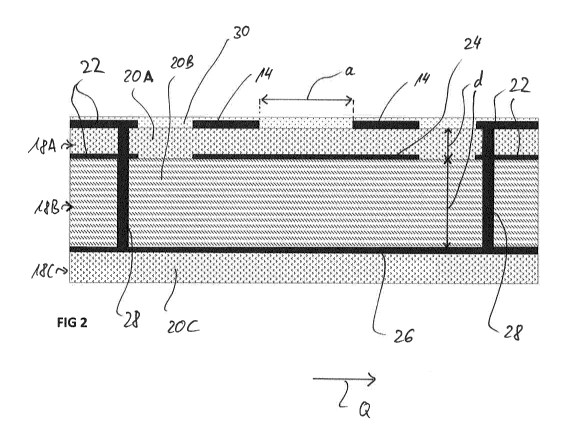
As can be seen from fig. 2, the printed circuit board 8
has a design with three layers 18A, B, C. In this case,
a respective layer 18A, B, C is formed by a support or
a substrate layer 20A, B, C on which respective
conductor track regions are formed. The topmost layer
18A has the signal conductors 14 formed on it, and
ground regions 22 at the edge. The first layer 18A can
therefore also be referred to as a signal conductor
layer. The middle substrate layer 20B has a conductor
track placed on it in the center, which forms a
decoupling line 24. To the side of this, ground regions
22 are again formed. The middle layer 18B can therefore
also be referred to as a decoupling layer. The
bottommost substrate layer 200 has had a preferably
all-over conductive coating added to it that forms a
ground layer and hence a ground conductor 26. During
operation, the ground conductor 26 is connected to
ground potential. The bottommost layer 180 can
therefore also be referred to as a ground layer.
As can be seen very clearly from fig. 2, the individual
substrate layers 20A, B, C have different layer
thicknesses d, the layer thickness d of the substrate
layer 20A, which is arranged between the signal
conductors 14 and the decoupling line 24, being smaller
than the thickness d of the subsequent middle substrate
layer 20B. The decoupling line 24 is therefore
insulated from the signal conductors 14 by means of the
substrate layer 20A, and there is no electrically
conductive connection made. Preferably, the first
CA 02945623 2016-10-13
- 16 -
substrate layer 20A has a thickness d in the region of
approximately 100 pm and the second substrate layer 20B
has a thickness d in the region of, by way of example,
300 pm.
The ground regions 22 of the different layers 18A, 18B
are in electrical contact with the ground conductor 26
through a multiplicity of plated-through holes 28. As
is evident particularly from the plan views of fig. 3A,
3B and 30, a multiplicity of such plated-through holes
28 are formed along all of the ground regions 22 in the
longitudinal direction of the printed circuit board.
The individual plated-through holes 28 are at a
distance of just a few mm or less from one another.
As revealed by fig. 2, the two signal conductors 14 are
arranged at a distance a from one another. They each
have a conductor track width of typically 100 to 200 pm
and preferably of approximately 175 pm. The distance a
between the two signal conductors is a little greater
and is typically 250 pm.
The decoupling conductor 24 arranged beneath the signal
conductors 4 extends in the transverse direction Q over
the two signal conductors 14, the edges of the
decoupling conductor 24 preferably being flush with the
outermost edges of the two signal conductors 14. The
decoupling conductor 24 therefore has an overall width
that corresponds to the width of the two signal
conductors plus the distance a between them.
Preferably, the width of the decoupling conductor 24 is
in the range between 500 and 750 pm, particularly being
600 pm.
The topmost layer 18A is also covered by an insulating
layer 30 that is preferably formed by a solder resist.
The representations of figs. 3A, 3B and 30 each show
the same detail. By placing the respective
CA 02945623 2016-10-13
- 17 -
representations on top of one another, the relative
orientation of the individual conductor track regions
of the individual layers 18A, B, C in relation to one
another is therefore obtained.
In this case, the detail representations of fig. 3A, 3B
and 30 show just a subregion of the printed circuit
board 8, specifically just the subregion of the
receiver paths that are provided with the decoupling
line 24. This is usually also followed by a printed
circuit board region with the transmitter paths.
Fig. 3A shows a detail from a plan view of the first
layer 18A. Fig. 2 showed only a sectional
representation in the region of a conductor pair with
two signal conductors 14. Fig. 3A now shows a plan view
of two such conductor pairs with a total of four signal
conductors 14. In this case, a respective conductor
pair is designed to transmit a differential signal. As
is clearly revealed, respective adjacent signal
conductors 14 forming a conductor pair are isolated by
a ground region 22, so that a respective conductor pair
is enclosed on both sides by ground regions 22.
A respective conductor track of the signal conductor 14
extends from an end pad 32 to an opposite pad 32. By
way of example, the pads 32 are each formed by widened
conductor track regions that may be additionally
coated. In this case, the individual signal conductors
14 do not run exactly linearly but rather also have
oblique conductor sections 33, as a result of which the
total length of the signal conductors 14 is increased
in comparison with a linear profile for a prescribed
length of the printed circuit board 8. The total length
of the printed circuit board is typically in the region
of approximately 20 mm.
The topmost layer 18A has had different electronic
components added that are connected firstly to the
CA 02945623 2016-10-13
- 18 -
signal conductors 14 or to the decoupling line 24 and
to the ground conductor 26.
Thus, as first components, DC isolating capacitors 34
are integrated in a respective signal conductor 14. To
this end, relevant contact feet of the isolating
capacitors 34 are connected to relevant pads of the
signal conductors 14. On account of the physical size
of these components, there is provision in this case
for the distance a between the two signal conductors 14
to be increased in the region of these isolating
capacitors 34. In this region, the distance a widens by
virtue of a y-shaped or funnel-shaped flare in the
signal conductors 14. Directly after the isolating
capacitors 34, there is a correspondingly symmetrical
taper to the original distance a.
Additionally, the topmost layer 18A has attenuating
elements 36 arranged on it in the form of nonreactive
resistances. In this case, each decoupling line 24 has
a respective associated attenuating element 36 of this
kind at the opposite ends of said decoupling line. The
ends of each of the attenuating elements 36 are thus in
electrical contact with the decoupling line 24 at
opposite ends thereof.
These assemblies 36 also have the distance a between
the signal conductors 14 widened. As a result, the
attenuating element 36 is accommodated symmetrically
between the signal conductors 14 of a respective
conductor pair.
The attenuating element 36 has two respective
connection regions that are at a distance from one
another in the longitudinal direction. In order now to
allow the largest possible coupling path and hence the
greatest possible length for the decoupling line 24 up
until connection of the attenuating elements 36, the
respective external connection region of the
CA 02945623 2016-10-13
- 19 -
attenuating element 36 is in electrical contact with
the decoupling line 24. To this end, an aperture or a
plated-through hole 28 is formed in the topmost
substrate layer 20A in order to make contact between
the attenuating element 36 and the underlying
decoupling line 24.
By contrast, the connection region directed inward
toward the center of the printed circuit board is in
contact with the ground conductor 26 of the bottommost
layer 18C via a plated-through hole 28.
As can be seen particularly from fig. 3B, the
decoupling line 24 has, to this end, an aperture 38
formed in it through which the plated-through hole 28
is routed. In the region of the attenuating elements
36, the decoupling line has a widened conductor track
width, so that there is sufficient space firstly for
making electrical contact and secondly also for making
the aperture 38.
As is additionally revealed by the plan view of fig.
3B, the respective decoupling line 24 has a taper 40,
formed in the style of a constriction, in the region of
the isolating capacitors 34. In the region of this
taper 40, the conductor track width is reduced. Figs.
3B and 3C show the electronic assemblies 34, 36 once
again to improve clarity. Their physical arrangement is
just on the topmost substrate layer 20A, however.
As can be seen therefrom, the profile of the decoupling
line 24 follows the profile of the signal conductors 14
exactly. The decoupling line 24 therefore runs parallel
to the signal conductors and follows the profile
thereof. Just in the transition regions, where the
distance a between the two signal conductors 8 varies
on account of the arrangement of the components,
particularly in the case of the isolating capacitors
34, there is a departure from the rigidly parallel
CA 02945623 2016-10-13
- 20 -
profile. However, the decoupling line 24 is in rigidly
symmetrical form, specifically, at each longitudinal
position, in relation to the two signal conductors 14.
As seen in a cross sectional plane, the decoupling line
24 is therefore at the same distance from each of the
two signal conductors 14. As is additionally revealed
by fig. 3B, the ground regions 22 also follow the
profile of the signal conductors 14, so that overall a
highly symmetrical embodiment of the conductor track
layout is achieved.
Finally, fig. 30 clearly reveals that the ground
conductor 26 is in the form of an extensive ground
plane that covers at least a large part of the printed
circuit board area.
During operation with data cable 4 connected and with
high speed data transmission, each conductor pair is
used to transmit a differential data signal SD. For
example on account of the pair shielding 16 described
at the outset, which is in the form of a longitudinally
folded foil, what are known as common mode signals Sc
are also included, which are undesirable for the actual
signal transmission. These signal components are
likewise coupled into the signal conductors 14 as well.
The special structure and the special design described
in the present case selectively decouple, in the manner
of a directional coupler, at least a subregion of the
common mode signal components Sc into the decoupling
line 24. The energy of these decoupled signal
components is consumed in the attenuating elements 36.
Therefore, the decoupling structure with the decoupling
line 24 and the attenuating elements 36 effectively
forms a sump for the undesirable signal components and
thereby results in improved signal transmission
overall.
CA 02945623 2016-10-13
- 21 -
The graph shown in fig. 4 shows an example of a modeled
profile of different variables. The results are based
on the following test setup:
The thickness d of the topmost substrate layer 20A is
100 pm, and the thickness d of the middle substrate
layer 20B is 300 pm. The topmost substrate layer 20A
has a dielectric constant Er of approximately 3.4. The
attenuating elements used were nonreactive resistances
having a resistance value of 22 ohms. The isolating
capacitors 34 have a rated capacitance of 100 nF.
What has been ascertained according to fig. 4 is the
profile of the attenuation of the differential signal
components SD over frequency, the profile of the common
mode signal components Sc over frequency and what is
known as the mode conversion M over frequency,
respectively. Additionally, a common mode
characteristic impedance of 50 ohms has been assumed.
Generally, mode conversion is understood to mean the
conversion of differential signal components SD into
common mode signal components Sc, and vice versa. Such
mode conversion is fundamentally undesirable.
In this case, the left-hand y axis shows the
attenuation values in dB for the differential signal
component SD and the common mode signal component Sc. By
contrast, the right-hand y axis shows the attenuation
values dB for the mode conversion.
As is clearly revealed, there is only slight
attenuation of the differential signal component SD
that is actually of interest over the entire frequency
spectrum from 0 to 30 GHz. The attenuation increases as
frequency increases, and reaches approximately -1 dB at
approximately 25 GHz.
By contrast, a very severe attenuation of the common
mode signal component Sc is identifiable, which
CA 02945623 2016-10-13
- 22 -
exhibits multiple maxima. In the case of the design
chosen in the present case with a length of
particularly approximately 14 mm for the decoupling
line 24, a local attenuation maximum of approximately
-3.2 dB is reached at approximately 3 GHz. The common
mode signal component Sc has further local attenuation
maxima at approximately 6 GHz and 10 GHz.
Overall, therefore, the printed circuit board design
with the decoupling structure that is described in the
present case achieves effective attenuation of the
undesirable common mode signal component Sc. A crucial
aspect in this context is that the arriving common mode
components are not reflected but rather are even
absorbed by the decoupling structure. Further studies
have also shown that this design is also distinguished
by a very good matching ratio, that is to say only low
reflection of the common mode signal components Sc back
into the connected data cable 4. A crucial aspect is
that the signal components Sc are absorbed. In the
present case, this is achieved especially effectively
particularly for frequency ranges between 1 and 5 GHz,
particularly in a region of approximately 3 GHz. The
printed circuit board 8 described in the present case
is fitted particularly in what is known as a QSFP
connector as what is known as a QSFP paddle card.
CA 02945623 2016-10-13
- 23 -
List of reference symbols
2 Connector
4 Data cable
6 Connector housing
8 Printed circuit board
Sheath
12 Wire pair
14 Signal conductor
10 16 Pair shielding
18A, B, C Layer
20A, B, C Substrate layer
22 Ground region
24 Decoupling line
26 Ground conductor
28 Plated-through hole
30 Insulating layer
32 Pad
33 Oblique conductor sections
34 Isolating capacitor
36 Attenuating element
38 Aperture
40 Taper
d Layer thickness
a Distance
SD Differential signal component
Sc Common mode signal component
Mode conversion
L Longitudinal direction
Transverse direction