Note: Descriptions are shown in the official language in which they were submitted.
81800596
1
ULTRASONIC IMAGING COMPRESSION METHODS AND APPARATUS
[0001]
FIELD
[0002] Aspects of the present disclosure relate to ultrasonic imaging
devices and
methods.
BACKGROUND
[0003] Conventional ultrasonic scanners generally include discrete
transducers and
control electronics. The control electronics are typically not integrated with
the
transducers, but rather are formed and housed separately.
[0004] Ultrasound transducer probes used for medical applications
typically
produce a large amount of data, as needed to produce ultrasound images for
medical
applications. The higher the quality and complexity of images desired, the
more data is
typically needed. Typically, the data is transferred from the transducer probe
to the
separately housed control electronics using cabling.
SUMMARY
[0005] The present disclosure details various aspects of an architecture
for on-chip
compression of data acquired using an ultrasonic transducer-based imager. In
some
embodiments, on-chip signal processing (e.g., data compression) may be
employed in the
receive signal path, for example, to reduce data bandwidth. For example, some
on-chip
compression architectures described herein may be configured to compress full
real-time
3D ultrasound imaging data to an extent that the compressed data may be
transferred
off-chip as a digital data stream using a consumer grade interface (e.g., USB
3.0, USB 3.1,
USB 2.0, Thunderbolt, Firewire, etc.). The digitization of received signals on-
chip allows
advanced digital signal processing to be performed on-chip, and thus permits
complete or
substantially
Date Recue/Date Received 2021-09-20
CA 02946137 2016-10-17
WO 2015/161164
PCT/US2015/026315
2
complete integration of an entire ultrasonic imaging system on a single
semiconductor
substrate. In some embodiments, a complete "ultrasound system on a chip"
solution is
provided.
[0006] Some embodiments are directed to a method for processing a signal
output
from an ultrasonic transducer element. The method comprises with a component
integrated
on a same semiconductor die as the ultrasonic transducer element, producing a
compressed
signal by compressing the signal output from the ultrasonic transducer
element, wherein the
compressed signal is configured to be transmitted out of the semiconductor die
as a data
stream.
[0007] Some embodiments are directed to a method, comprising performing on-
chip
compression of a plurality of ultrasound signals produced by an array of
ultrasonic
transducers integrated with the chip.
[0008] Some embodiments are directed to an ultrasound device, comprising at
least
one ultrasonic transducer element integrated on a semiconductor die; and a
compression
circuit, integrated on the semiconductor die, configured to compress a signal
output from the
at least one ultrasonic transducer element, wherein the compressed signal is
configured to be
transmitted out of the semiconductor die as a data stream.
[0009] Some embodiments are directed to an ultrasound device, comprising at
least
one ultrasonic transducer element integrated on a semiconductor die; and an
image
reconstruction circuit, integrated on the semiconductor die, configured to
perform at least a
portion of an image reconstruction process based, at least in part, on a
signal output from the
at least one ultrasonic transducer element.
[0010] Some embodiments are directed to a method, comprising performing at
least a
portion of an on-chip image reconstruction process based, at least in part, on
a signal output
from at least one ultrasonic transducer integrated with the chip.
[0011] Some embodiments are directed to a method for processing a signal
output
from an ultrasonic transducer element. The method comprises with a component
integrated
on a same semiconductor die as the ultrasonic transducer element, performing
at least a
portion of an image reconstruction process based at, least in part, on the
signal output from
the at least one ultrasonic transducer element.
[0012] Some embodiments are directed to an ultrasound device comprising at
least
one ultrasonic transducer element integrated on a semiconductor die and
configured to
81800596
3
generate an imaging signal; control circuitry configured to produce multiple
imaging
modes of operation of the ultrasound device; and compression circuitry,
integrated on the
semiconductor die, configured to compress the imaging signal utilizing one of
a plurality
of compression schemes, based, at least in part, on a selected imaging mode of
operation.
[0013] Some
embodiments are directed to a method for processing a signal output
from at least one ultrasonic transducer element. The method comprises
determining an
imaging mode of operation of an ultrasound device comprising the at least one
ultrasonic
transducer element; and compressing data recorded by the ultrasound device
using one of a
plurality of compression schemes selected, based, at least in part, on the
determined (e.g.,
programmed) imaging mode of operation.
[0013a] According to one aspect of the present invention, there is provided an
ultrasound device, comprising: at least one ultrasonic transducer element
integrated on a
semiconductor die; an analog to digital converter (ADC) integrated on the
semiconductor
die, wherein the ADC is configured to process a signal output from the at
least one
ultrasonic transducer element to produce a digital signal; and a compression
circuit
integrated on the semiconductor die and configured to generate a compressed
signal by
compressing the digital signal, wherein the compressed signal is configured to
be
transmitted out of the semiconductor die as a data stream, wherein the
compression circuit
comprises a filter, a decimation circuit, a re-quantization circuit, and an
arithmetic logic
unit (ALU), wherein an output of the filter is coupled to an input of the
decimation circuit,
an output of the decimation circuit is coupled to an input of the re-
quantization circuit, and
an output of the re-quantization circuit is coupled to an input of the ALU;
and wherein the
compression circuit is configured to generate the compressed signal prior to
any image
reconstruction process.
[0013131 According to another aspect of the present invention, there is
provided a
method for processing a signal output from an ultrasonic transducer element,
comprising:
with a component integrated on a same semiconductor die as the ultrasonic
transducer
element, processing the signal output from the ultrasonic transducer element
to produce a
digital signal; and with at least one additional component integrated on the
semiconductor
die, producing a compressed signal by compressing the digital signal, wherein
the
compressed signal is configured to be transmitted out of the semiconductor die
as a data
stream, wherein compressing the digital signal comprises filtering the digital
signal with a
Date Recue/Date Received 2021-09-20
81800596
3a
filter integrated on the semiconductor die to produce a filtered signal,
decimating the
filtered signal with a decimation circuit integrated on the semiconductor die
to produce a
decimated signal, re-quantizing the decimated signal with a re-quantization
circuit
integrated on the semiconductor die to produce a re-quantized signal, and
processing the
re-quantized signal with an arithmetic logic unit (ALU) integrated on the
semiconductor
die; and wherein the compression circuit is configured to generate the
compressed signal
prior to any image reconstruction process.
[0014] It should be appreciated that all combinations of the foregoing
concepts and
additional concepts discussed in greater detail below (provided that such
concepts are not
mutually inconsistent) are contemplated as being part of the inventive subject
matter
disclosed herein.
BRIEF DESCRIPTION OF THE DRAWINGS
[0015] Various aspects and embodiments of the disclosed technology will
be
described with reference to the following figures. It should be appreciated
that the figures
are not necessarily drawn to scale. Items appearing in multiple figures are
indicated by the
same reference number in all the figures in which they appear.
[0016] Fig. 1A shows an illustrative architecture block diagram of an
ultrasonic
imaging device in accordance with embodiments of the present disclosure;
[0017] Fig. 1B shows the illustrative architecture of Fig. 1A when
integrated with
additional components, in accordance with some embodiments of the present
disclosure;
[0018] Fig. 2 shows a schematic illustration of the arrangement of
individually-
controllable modules of ultrasonic transducer elements in an array used in
accordance with
some embodiments of the present disclosure;
[0019] Fig. 3 shows an alternative illustrative architecture in which at
least some
digital processing components are located off-chip, in accordance with some
embodiments
of the present disclosure;
Date Recue/Date Received 2021-09-20
CA 02946137 2016-10-17
WO 2015/161164
PCMJS2015/026315
4
[0020] Fig. 4 shows an illustrative architecture for a time gain
compensation circuit
that may be used in accordance with some embodiments of the present
disclosure;
[0021] Fig. 5 shows an illustrative architecture for a data reduction
circuit that may be
incorporated in some embodiments of the present disclosure;
[0022] Fig. 6 shows an illustrative architecture for data reduction within
a digital
processing block of the data reduction circuit shown in Fig. 5;
[0023] Fig. 7 shows an illustrative architecture for a cascade integrating
comb circuit
that may be used in accordance with some embodiments of the present
disclosure;
[0024] Fig. 8 shows an illustrative circuit for performing data reduction
in accordance
with some embodiments of the present disclosure;
[0025] Fig. 9 shows an illustrative circuit for performing quadrature
downsampling
by a factor of four in accordance with some embodiments of the present
disclosure;
[0026] Fig. 10 shows an alternative circuit for performing quadrature
downsampling
by a factor of four in accordance with some embodiments of the present
disclosure;
[0027] Fig. 11 shows an alternative circuit for performing quadrature
downsampling
by a factor of four in accordance with some embodiments of the present
disclosure;
[0028] Fig. 12 shows an alternative circuit for performing quadrature
downsampling
by a factor of four in accordance with some embodiments of the present
disclosure;
[0029] Fig. 13 shows an illustrative architecture for a polyphase filter
that may be
used in accordance with some embodiments of the present disclosure;
[0030] Fig. 14 shows an illustrative architecture for an arithmetic logic
unit that may
provide data reduction in accordance with some embodiments of the present
disclosure;
[0031] Fig. 15 shows an illustrative architecture for image formation using
an
integrated backprojection technique in accordance with some embodiments of the
present
disclosure;
[0032] Fig. 16 shows an alternative architecture for image formation using
an
integrated backprojection technique in accordance with some embodiments of the
present
disclosure;
[0033] Fig. 17 shows an illustrative architecture for performing ensemble
compression in accordance with some embodiments of the present disclosure;
CA 02946137 2016-10-17
WO 2015/161164 PCMJS2015/026315
[0034] Figs. 18A and 18B show illustrative architectures for performing
dynamic
focusing using streaming addressable and pipeline delays, respectively, in
accordance with
some embodiments of the present disclosure; and
[0035] Fig. 19 is a flowchart of an illustrative process for operating an
ultrasonic
transducer array, in accordance with some embodiments of the present
disclosure.
DETAILED DESCRIPTION
[0036] Applicants have appreciated that the lack of integration of the
transducers and
control circuitry of conventional ultrasound scanners is demanded in part by
the large amount
of data collected by ultrasound transducer probes and used to generate
ultrasound images.
Correspondingly, Applicants have appreciated that suitable device
configurations and
techniques for reducing or otherwise handling such large amounts of data while
still allowing
for generation of desired ultrasound image types at suitable quality would
facilitate the
attainment of integrated ultrasound devices having ultrasonic transducers and
control
electronics in a compact form. The present disclosure addresses this issue by
providing
unique, cost-effective, and scalable integrated data compression architectures
to reduce data
bandwidth while providing data that is sufficiently robust for advanced
imaging applications.
Thus, aspects of the present application provide an architecture which may be
used with a
single substrate ultrasound device having integrated ultrasonic transducers
(e.g., CMOS
ultrasonic transducers) and circuitry.
[0037] Accordingly, some aspects of the present disclosure provide new
apparatuses,
systems, and methods that push the forefront of ultrasound image processing by
providing a
robust and highly integrated "ultrasound system on a chip" with direct
integration of
ultrasonic transducer arrays fabricated on the same die as a fully digital
ultrasound front-end.
As used herein, "fabricated/integrated on the same die" means integrated on
the same
substrate or integrated using one or more stacked die integrated with 3D chip
packaging
technology. According to some aspects of the present disclosure, these
architectures may
allow sufficient access to digitized channels that maintain independent data
to permit the use
of state-of-the-art, off-the-shelf computing platforms for performing
sophisticated image
formation and/or processing algorithms. In at least some embodiments, high-
resolution 3D
volumetric imaging, as just one example, may be performed using the devices
and techniques
for data reduction and handling described herein.
CA 02946137 2016-10-17
WO 2015/161164 PCMJS2015/026315
6
[0038] Fig. lA shows an illustrative example of an integrated ultrasound
device 100
embodying various aspects of the present disclosure. As shown, the device 100
includes a
plurality of circuits formed on a semiconductor die 112 including transmit
(TX) control
circuit 104, analog receive (RX) circuit 103, receive (RX) compression circuit
130, and
receive (RX) buffer memory 140. Each of these circuits may include one or more
additional
circuits. For example, TX control circuit 104 may include TX waveform
generators, TX
parameter and control registers, analog pulsar circuitry to drive an array of
acoustic elements
and/or circuitry implementing a delayed waveform distribution function.
[0039] Fig. 1B shows the ultrasound device 100 of Fig. 1A, including the
elements
shown in Fig. lA with additional elements incorporated on semiconductor die
112. For
example, device 100 in Fig. 1B additionally includes one or more transducer
arrangements
(e.g., arrays) 102, a timing & control circuit 108, and a power management
circuit 118.
[0040] Analog RX circuit 103 may include analog signal chain components
that
process signals output from a plurality of ultrasonic transducer elements. The
ultrasonic
transducers of the ultrasonic transducer elements may be of any suitable type,
and in some
embodiments are capacitive micromachined ultrasound transducers (CMUTs), which
may
allow for fabrication of high quality ultrasonic transducers in the same
semiconductor
foundries that are currently driving the electronics industry. Such CMUTs may
be formed in
and/or formed on the same substrate as the integrated circuitry (e.g., a
silicon substrate).
[0041] In one aspect, analog RX circuit 103 may include a plurality of rows
(e.g., four
rows). Each row may include analog signal chain elements (e.g., 144 elements)
for a full
column of sensors in an ultrasound transducer array. In some embodiments, one
or more
components (e.g., an automatic gain control component) in analog RX circuit
103 may be
controlled by a time gain compensation (TGC) circuit 160 that compensates for
signals
received from different depths in an imaged object (e.g., by providing
variable gain based on
the timing at which the signal is received). TGC circuit 160 may be included
as a portion of
RX compression circuit 130 described below. An illustrative architecture for
TGC circuit
160 is discussed in more detail below with respect to Fig. 4.
[0042] RX compression circuit 130 may include circuits for processing
outputs from
analog RX circuit 103. In some implementations, RX compression circuit 130 may
include
circuits configured to reduce a data bandwidth of data received from analog RX
circuit 103,
as discussed in more detail below. For example, RX compression circuit 130 may
include
CA 02946137 2016-10-17
WO 2015/161164 PCMJS2015/026315
7
circuits configured to process the received data by filtering, averaging,
sampling, decimating,
and/or using other techniques to provide on-chip compression to enable the
processed data to
be transmitted off-chip at a desired data rate. RX compression circuit 130 may
include
analog and/or digital components for performing data compression, and
embodiments are not
limited based on whether particular aspects of the compression circuitry is
implemented using
an analog architecture, a digital architecture, or using a combination of
analog and digital
components. For example, the digital mixing circuitry described in more detail
below may
alternatively be implemented using an analog heterodyning circuit to provide
equivalent
functionality. Additionally, other features including, but not limited to,
channel summation,
dynamic delay, and frequency filtering may be implemented using digital and/or
analog
components, and embodiments are not limited in this respect.
[0043] RX compression circuit 130 may also include other components
including RX
control and parameter registers. Additionally, RX compression circuit 130 may
be associated
with at least one microprocessor (not shown) integrated on die 112 that may be
used, at least
in part, to compress the digital signals processed by RX compression circuit
130.
[0044] RX buffer memory 140 may be configured to temporarily store the
output of
RX compression circuit 130 prior to transmitting the data off-chip, as
discussed in further
detail below.
[0045] Components included in some embodiments as a portion of RX
compression
circuit 130 are also shown. As discussed above, some embodiments of the
present disclosure
provide data compression architectures to facilitate the transfer of data off
of semiconductor
die 112 as a data stream at a data rate compatible with output interface 114
having a
maximum data bandwidth. In some embodiments, the data stream may be a serial
data
stream. Components of RX compression circuit 130 (also referred to herein as
"compression
circuitry") may be configured to provide data compression using one or more
data
compression techniques, examples of which are described herein. RX compression
circuit
130, as shown, includes an RX control circuit 106 and a signal
conditioning/processing
circuit 110. RX control circuit 106 further includes a data reduction circuit
132 configured to
process data received from analog signal chain elements of analog RX circuitry
103. Data
reduction circuit 132, discussed in more detail below, may include circuitry
configured to
perform data compression on signals prior to performing at least a portion of
an image
reconstruction process. In some embodiments, at least some outputs of data
reduction circuit
132 may be provided to buffer memory 140 without being further processed by
signal
CA 02946137 2016-10-17
WO 2015/161164 PCMJS2015/026315
8
conditioning/processing circuit 110, as represented by the optional data path
between data
reduction circuit 132 and buffer memory 140.
[0046] In the example shown, data reduction circuit 132 may include analog
compression circuitry, an analog-to-digital converter (ADC), and digital
compression
circuitry. The ADC may, for example, comprise a 10-bit, 1, 5, 10, or 20 mega-
samples per
second (Msps), 40 Msps, 50 Msps. or 80 Msps ADC. The ADC may alternatively
have any
desired resolution including, but not limited to, 1-bit, 4-bit, 16-bit, or 20-
bit. Illustrative
types of ADCs that may be used include, but are not limited to, a successive
approximation
register (SAR) ADC, a flash ADC, a pipeline ADC, a sigma-delta ADC, a multi-
slop ADC,
and a time-interleaved ADC. In some embodiments, the ADC may be sampling at a
lower
rate than the center frequency of the received signal, thereby aliasing
relevant data.
[0047] After undergoing processing in the data reduction circuit 132, the
outputs of
all of the RX control circuits 106 (the number of which, in this example, is
equal to or less
than the number of transducer elements on the chip) may be transmitted to a
multiplexer
(MUX) 142 in the signal conditioning/processing circuit 110. In some
embodiments, the
number of RX control circuits may be different than the number of transducer
elements on
the chip, and embodiments of the present disclosure are not limited in this
respect. The MUX
142 multiplexes the digital data from the various RX control circuits 106, and
the output of
the MUX 142 may optionally be provided to digital signal processing block 150
in the signal
conditioning/processing circuit 110 prior to outputting the data from the die
112, e.g., via one
or more output ports 114. Some embodiments may not include MUX 142, and
outputs from
the RX control circuits 106 may be provided directly to digital signal
processing block 150
and/or stored in buffer 140 prior to being sent off the chip.
[0048] As shown, digital signal processing block 150 includes image
formation
circuit 134 configured to perform at least a portion of an image
reconstruction process, and
the output of the image formation circuit 134 may be output off-chip for
further processing
and/or display. Digital signal processing block 150 may also include post-
processing circuit
136 that operates on the output of image formation circuit 134 to provide
additional data
compression. Illustrative architectures for each of data reduction circuit
132, image
formation circuit 134, and post-processing circuit 136 that may be formed on a
semiconductor die 112 as a portion of an ultrasound imager in accordance with
embodiments
of the present disclosure are discussed in more detail below. In some
embodiments,
discussed in more detail below, all or a portion of digital signal processing
block 150 may be
CA 02946137 2016-10-17
WO 2015/161164 PCMJS2015/026315
9
formed off-chip, and data from one or more RX control circuits 106 may be
stored in buffer
memory 140 without processing by signal conditioning and processing circuit
110.
[0049] As explained in more detail below, various components in RX
compression
circuit 130 may serve to decouple waveforms from the received signal and
otherwise reduce
the amount of data that is output from the die 112 via a data link or
otherwise. The inclusion
of such elements may thus further facilitate and/or enhance an -ultrasound-on-
a-chip"
solution in accordance with some embodiments.
[0050] In the embodiment shown in Fig 1B, all of the illustrated components
are
formed on a single semiconductor die 112 or are formed on multiple stacked
integrated dice
using 3D packaging technology. It should be appreciated, however, that in
alternative
embodiments one or more of the illustrated elements may be instead located off-
chip, as
discussed in more detail below in connection with Fig. 3. In addition,
although the illustrated
example shows both a TX control circuit 104 and an RX control circuit 106, in
alternative
embodiments only a TX control circuit or only an RX control circuit may be
employed. For
example, such embodiments may be employed in a circumstance where one or more
transmission-only devices 100 are used to transmit acoustic signals and one or
more
reception-only devices 100 are used to receive acoustic signals that have been
transmitted
through or reflected by a subject being ultrasonically imaged.
[0051] Fig. 2 shows an embodiment of ultrasound device 100 comprising a
substrate
202 that includes multiple ultrasound circuitry modules 204 formed thereon. As
shown, an
ultrasound circuitry module 204 may comprise multiple ultrasound elements 206.
An
ultrasound element 206 may comprise multiple ultrasonic transducers 208. Such
a modular
design allows for scalability of the architecture to any desired size or
arrangement.
[0052] In the illustrated embodiment, substrate 202 comprises 144 modules
arranged
as an array having 72 rows and two columns. However, it should be appreciated
that a
substrate of an ultrasound device 100 may comprise any suitable number of
ultrasound
circuitry modules (e.g., at least two modules, at least ten modules, at least
100 modules, at
least 1000 modules, at least 5000 modules, at least 10,000 modules, at least
25,000 modules,
at least 50,000 modules, at least 100,000 modules, at least 250,000 modules,
at least 500,000
modules, between two and a million modules. etc.) that may be arranged as an
two-
dimensional array of modules having any suitable number of rows and columns or
the
ultrasound circuitry modules may be arranged in any other suitable way.
CA 02946137 2016-10-17
WO 2015/161164
PCMJS2015/026315
[0053] In the illustrated embodiment, each module 204 comprises 64
ultrasound
elements arranged as an array having two rows and 32 columns. However, it
should be
appreciated that an ultrasound circuitry module 204 may comprise any suitable
number of
ultrasound elements (e.g., one ultrasound element, at least two ultrasound
elements, at least
four ultrasound elements, at least eight ultrasound elements, at least 16
ultrasound elements,
at least 32 ultrasound elements, at least 64 ultrasound elements, at least 128
ultrasound
elements, at least 256 ultrasound elements, at least 512 ultrasound elements,
between two and
1024 elements, etc.) that may be arranged as a two-dimensional array of
ultrasound elements
having any suitable number of rows and columns or in any other suitable way,
[0054] In the illustrated embodiment, each ultrasound element 206 comprises
16
ultrasonic transducers arranged as a two-dimensional array having four rows
and four
columns. However, it should be appreciated that an ultrasound element 206 may
comprise
any suitable number of ultrasonic transducers (e.g., one, at least two, at
least four, at least 16,
at least 25, at least 36, at least 49, at least 64, at least 81, at least 100,
between one and 200,
etc.) that may be arranged as a two dimensional array having any suitable
number of rows
and columns (square or rectangular) or in any other suitable way.
Alternatively, the
ultrasonic transducers may be arranged in any other suitable geometric array
including, but
not limited to, a hexagonal array, a triangular array, and a skewed lattice.
[0055] Each ultrasound circuitry module 204 may comprise or be associated
with
circuitry in addition to one or more ultrasound elements. For example, an
ultrasound
circuitry module may comprise circuitry associated with transmitting acoustic
waves
including, but not limited to, one or more waveform generators (e.g., two
waveform
generators, four waveform generators, etc.), encoding circuitry, and decoding
circuitry. In
some embodiments, all or a portion of an ultrasound circuitry module may
additionally or
alternatively comprise or be associated with any other suitable circuitry. For
example, in
some embodiments, each module 204 may be associated with receive-side
components
including, but not limited to, analog signal chain elements and digital signal
processing
elements, as described briefly above, and described in more detail below.
[0056] In some embodiments, each module may include eight receive channels,
and
each of the eight receive channels may be associated with a single timing and
control circuit
or other control elements including, but not limited to, a time gain
compensation circuit, as
discussed in more detail below. Additionally, each module may be associated
with multiple
components to perform analog and/or digital signal processing to output
signals from the
receive channels of the module. For example, such components may include, but
are not
CA 02946137 2016-10-17
WO 2015/161164
PCMJS2015/026315
11
limited to, components of the analog receive chain and components of the
digital signal
processing circuitry such as memory, multiplier circuits, and adder circuits.
[0057] In some embodiments, the ultrasound device may comprise module
interconnection circuitry integrated with the substrate and configured to
connect ultrasound
circuitry modules to one another to allow data to flow among the ultrasound
circuitry
modules. For example, the device module interconnection circuitry may provide
for
connectivity among adjacent ultrasound circuitry modules. In this way, an
ultrasound
circuitry module may be configured to provide data to and/or receive data from
one or more
other ultrasound circuitry modules on the device.
[0058] It should be appreciated that communication between one or more of
the
illustrated components may be performed in any of numerous ways. In some
embodiments,
for example, one or more high-speed busses (not shown), such as that employed
by a unified
Northbridge, may be used to allow high-speed intra-chip communication or
communication
with one or more off-chip components. In some embodiments, one or more modules
may be
connected using an interconnection network. For example, a shift register ring
communication network may be used where neighboring modules communicate with
one
another via the network.
[0059] In some embodiments, timing & control circuit 108 may, for example,
be
responsible for generating all timing and control signals that are used to
synchronize and
coordinate the operation of the other elements in the device 100. In the
example shown, the
timing & control circuit 108 is driven by a single clock signal CLK supplied
to an input port
116. The clock signal CLK may, for example, be a high-frequency clock used to
drive one or
more of the on-chip circuit components. In some embodiments, the clock signal
CLK may,
for example, be a 1.5625GHz or 2.5GHz clock used to drive a high-speed serial
output device
(not shown in Fig. 1B) in the signal conditioning/processing circuit 110, or a
20 MHz, 40
MHz. or 200MHz (or any other suitable speed) clock used to drive other digital
components
on the die 112, and the timing & control circuit 108 may divide or multiply
the clock CLK, as
necessary, to drive other components on the die 112. In other embodiments, two
or more
clocks of different frequencies (such as those referenced above) may be
separately supplied
to the timing & control circuit 108 from an off-chip source.
[0060] In the example shown, one or more output ports 114 may output a data
stream
generated by one or more components of the signal conditioning/processing
circuit 110.
CA 02946137 2016-10-17
WO 2015/161164
PCMJS2015/026315
12
Such data streams may, for example, be generated by one or more USB 2.0
modules, one or
more USB 3.0 modules, one or more USB 3.1 modules, one or more Thunderbolt
modules,
one or more FireWire modules, and/or one or more Gigibit (e.g., 10GB, 40GB, or
100GB)
Ethernet modules, integrated on the die 112. In some embodiments, the signal
stream
produced on output port 114 can be provided as input to an electronics device
including, but
not limited to, a cloud service, one or more computers, a tablet, and/or a
smartphone. The
one or more electronic devices receiving the signal stream may generate and/or
display
numerical values, 1-dimensional, 2-dimensional, 3-dimensional, and/or
tomographic images.
In some embodiments, the signal stream output on output port 114 may be
provided to one or
more additional off-chip circuits for additional processing, as discussed
below in connection
with Fig. 3.
[0061] In embodiments in which image reconstruction capabilities are
incorporated in
the signal conditioning/processing circuit 110 (as explained further below),
even relatively
low-power devices, such as smartphones or tablets which have only a limited
amount of
processing power and memory available for application execution, can display
images using
only a data stream from the output port 114. Examples of high-speed serial
data modules and
other components that may be included in the signal conditioning/processing
circuit 110 are
discussed in more detail below. Performing at least a portion of an image
reconstruction
process on-chip and transmitting the output of the at least a portion of the
image
reconstruction process off-chip using a data link is one of the features that
may facilitate an
integrated "ultrasound on a chip" solution that can be used with a wide range
of external
display devices having varying degrees of processing power in accordance to
some
embodiments of the present disclosure.
[0062] In various embodiments, each RX control circuit 106 may be
associated with a
single transducer, a group of two or more transducers within a single
transducer element, a
single transducer element comprising a group of transducers, a group of two or
more
transducer elements within a module, a single module comprising two or more
transducer
elements, two or more modules in an array 102, or an entire array 102 of
transducers.
[0063] In the example shown in Fig. 1B, there is a separate RX control
circuit 106 for
each transducer in the array(s) 102, but there is only one instance of each of
the timing &
control circuit 108 and the signal conditioning/processing circuit 110.
Accordingly, in such
an implementation, the timing & control circuit 108 may be responsible for
synchronizing
and coordinating the operation of all RX control circuit 106 combinations on
the die 112, and
CA 02946137 2016-10-17
WO 2015/161164 PCMJS2015/026315
13
the signal conditioning/processing circuit 110 may be responsible for handling
inputs from all
of the RX control circuits 106 on the die 112. Alternatively, die 112 may
include multiple
timing & control circuits 108, with each of the timing & control circuits
being responsible for
synchronizing and coordinating the operation of a subset of RX control circuit
combinations
on the die.
[0064] As discussed above, in some embodiments, at least some of the
receive-path
digital signal processing electronics discussed above in connection with Fig.
1B, may be
implemented off-chip to reduce the size of the ultrasound-on-a-chip
architecture, to reduce
power consumption of the ultrasound device 100, or for any other reason
including, but not
limited to, providing advanced image reconstruction capabilities using one or
more off-chip
processors.
[0065] Fig. 3 shows an illustrative embodiment of ultrasound device 100 in
which a
portion of the receive-path digital signal processing circuitry is implemented
off-chip. In the
illustrated embodiment, field-programmable gate array (FPGA) 300 is connected
to portions
of device 100 implemented on substrate 112. FPGA 300 is configured to perform
at least
some signal processing operations described above as having been performed in
the
embodiment shown in Fig. 1B. For example, FPGA 300 may include processing unit
310
configured to receive imaging data from buffer memory 140 and perform image
reconstruction or any other suitable operation on the received imaging data.
Additionally,
FPGA 300 may be configured to transmit control data to the portion of
ultrasound device 100
integrated on substrate 112. The control data may include control parameters
to control
operation of transmit control circuitry 104 and/or receive-side circuitry
including, but not
limited to, analog TX circuitry 104, analog RX circuitry 103, and RX control
circuit 106.
FPGA 300 may be further configured to send processed imaging data to output
interface 314
for transmission to any suitable device for display and/or further processing,
as discussed
above. Any suitable data interface may be used to transfer data between die
112 and FPGA
300 using output port 114, and embodiments of the present disclosure are not
limited in this
respect. In some embodiments, a digital signal processor (DSP), an embedded
controller, or
any other digital circuit logic may be used in addition to, or as an
alternative to, FPGA 300
for providing at least a portion of the receive-path digital circuitry off-
chip.
[0066] As discussed above, in some embodiments, RX control circuitry 106
may
include a time gain compensation (TGC) circuit 160 configured to provide
digital control of
an analog variable gain amplifier (VGA) to process signal outputs from the
ultrasound
CA 02946137 2016-10-17
WO 2015/161164 PCMJS2015/026315
14
transducer elements. TGC circuit 160 compensates for signals received from
different depths
in an imaged object (e.g., by controlling the VGA to provide variable gain for
signals
received at different times).
[0067] In one embodiment, output from the VGA is stored in a memory, and
VGA
values are read from the memory at the TGC circuit update rate. Fig. 4
illustrates an example
architecture of a TGC circuit 160 that may be used in accordance with some
embodiments of
the present disclosure, and requires less memory and fewer programming words
than the
aforementioned embodiment that reads VGA values from memory at the update rate
of the
TCG circuit. The illustrated TGC circuit 160 is implemented as a multi-stage
summing
control circuit that controls an analog variable gain amplifier, which
amplifies signals
received from greater depths compared to signals received from shallower
depths. TGC
circuit 160 includes controlling circuitry elements including adder 410 and
delay element
420.
[0068] In some embodiments, TGC circuit 160 may be configured to model a
corrective gain profile for the variable gain amplifier with a piecewise
polynomial (i.e.,
composed of multiple polynomial segments). The gain profile may be designed
(manually by
a user and/or automatically) to match the signals output from the ultrasound
transducer
elements. The piecewise polynomial model may be of any order including, but
not limited to,
a third order polynomial model. One implementation for modeling a piecewise
polynomial is
to use three stages of an integrator circuit, as shown in Fig. 4. Other order
polynomials can
similarly be implemented by using more or less stages. In some embodiments,
the piecewise
polynomial is modeled using a variable input update rate, which is the rate at
which a control
signal for controlling a variable gain amplifier circuit is updated.
Illustrative input update
rates for updating the control signal include update rates ranging between 100
kHz and 1.25
MHz. or may include other suitable values including update rates ranging from
below 100
kHz to the update rate of an ADC on the chip (e.g., 50 MHz). In some
embodiments, the
spacing between updates of the control signal is non-uniform resulting in a
variable input
update rate. Other update rates including the calculation update rate and the
output update
rate may be based on internal registers and may be constant (e.g., 50 MHz, 100
MHz, or 200
MHz) or variable. In particular, the calculation update rate for updating the
polynomial
coefficients may be fixed or variable. It should be appreciated that any
suitable input,
calculation, and output update rates may alternatively be used.
CA 02946137 2016-10-17
WO 2015/161164
PCMJS2015/026315
[0069] In some embodiments, the parameterization of the variable gain
profile
provided by the TGC circuit 160 may be programmable, such that the piecewise
polynomial
function may be calculated dynamically, and may be programmed differently
based on a
selected imaging mode and/or imaging application. For example, in order to
program
multiple segments of a piecewise polynomial function, the parameters (e.g.,
x0, yO, zO, and
duration) may be changed dynamically during a TGC curve evaluation to
implement
subsequent polynomial segments. In some embodiments, all parameters (including
the
duration parameter) may be programmed for each piecewise segment of the
polynomial
function. Alternatively, a subset (i.e., fewer than all) of the parameters may
be changed
dynamically for each segment. For example, in one implementation, only the a0
parameter is
changed between polynomial segments. In some embodiments, each module (e.g.,
comprising eight receive channels) may be associated with a single TGC circuit
160.
Alternatively, multiple TGC circuits may be associated with each module, and
embodiments
are not limited in this respect.
Illustrative types of compression
[0070] Ultrasound imaging devices provided in accordance with some
embodiments
of the present disclosure record a large amount of ultrasound data to provide
quality images
using an array of ultrasonic transducer elements, as discussed above. To
process this large
amount of data and transfer the data off-chip at an acceptable rate using an
output data
interface module having a maximum data bandwidth, some embodiments employ on-
chip
circuitry to compress the data from the ultrasonic transducer elements prior
to transmitting
the data off-chip. The inclusion of on-chip data compression elements may thus
further
facilitate and/or enhance an "ultrasound-on-a-chip" solution in accordance
with some
embodiments.
[0071] In some embodiments, different types of compression may be selected
depending on the imaging goals and/or mode of operation of the ultrasound
imaging
application. For example, the different types or amounts of compression used
may depend, at
least in part, on an acceptable image quality for a particular imaging
application. Examples
of on-chip compression that may be implemented in accordance with embodiments
of the
present disclosure include, but are not limited to, spectral compression,
aperture compression,
excitation compression, ensemble compression, entropy compression, signal
value
compression, and selective omission compression, each of which is described in
more detail
below.
CA 02946137 2016-10-17
WO 2015/161164
PCMJS2015/026315
16
[0072] Spectral compression compresses data by operating on the frequency
content
of a received acoustic signal. Spectral compression downsizes an amount of
spectral
bandwidth to only that which is necessary to achieve a desired image
resolution. Examples
of spectral compression include, but are not limited to, quadrature
demodulation and filtered
downsampling, each of which is described in more detail below.
[0073] Aperture compression limits the cross-range bandwidth of the
acoustic signal
to only that which is needed to achieve a desired lateral image resolution.
Examples of
aperture compression include, but are not limited to, filtered downsampling
and other
filtering techniques described in more detail below.
[0074] Excitation compression compresses data by combining excitations in a
unique
way in which redundant information between excitations are compressed
together. A non-
limiting example of excitation compression is to form an image from the
excitations, where
all excitations have been compressed into one image reconstruction.
[0075] Ensemble compression reduces data redundancy in ensemble imaging by
calculating relevant information. A non-limiting example of ensemble
compression is
Doppler processing, described in more detail below, where multiple images are
compressed
into a single complex velocity and power reconstruction profile.
[0076] Entropy compression reduces information redundant in data
communication as
it is provided off-chip. Encoding frame-to-frame differences rather than
encoding the full
data for each frame is a non-limiting example of entropy compression.
[0077] Signal value compression reduces data to values corresponding to a
desired
interest in characteristics (e.g., power, max value, variance) of the overall
signal. Non-
limiting examples of signal value compression include compression circuitry
that calculates
the total power in a signal and compression circuitry that determines a time-
of-flight for
received acoustic signals for characterization processes.
[0078] Selective omission compression reduces an amount of data by
selectively
omitting data from the full set of data. Non-limiting examples of selective
omission
compression include re-quantization, described in more detail below, and
sparse aperture
imaging.
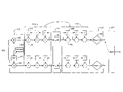
[0079] On-chip circuitry, discussed in more detail below, for performing
compression
of acoustic data signals received from an array of ultrasonic elements may be
implemented to
perform one or more of the types of compression discussed above. In some
embodiments, a
CA 02946137 2016-10-17
WO 2015/161164
PCMJS2015/026315
17
data signal may be compressed to be transmitted off-chip in accordance with
one or more
operating parameter requirements. For example, in some embodiments, the
compressed data
signal is compressed such that it may be transmitted out of the semiconductor
die as a data
stream at a rate of less than or equal to four Gigabits per second or at some
other suitable rate.
In some embodiments, the data signal may be compressed by a factor of greater
than one but
less than two. In some embodiments, the data signal may be compressed by at
least a factor
of two and less than a factor of four. In some embodiments, the data signal
may be
compressed by at least a factor of four and less than a factor of ten. In some
embodiments,
the data signal may be compressed by at least a factor of ten and less than a
factor of twenty.
In some embodiments, the data signal may be compressed by at least a factor of
twenty and
less than a factor of one hundred. In other embodiments, the data signal may
be compressed
by at least a factor of one hundred and less than a factor of one thousand. In
some
embodiments, the data signal may be compressed by at least a factor of one
thousand and less
than a factor of ten thousand. It should be appreciated that any suitable
amount of
compression may alternatively be used, and the ranges discussed above for
compression
amount are provided merely for illustrative purposes.
[0080] In some embodiments, the ultrasound imager may be configurable to
operate
in a plurality of imaging modes (e.g., 2D, 3D), and the type and/or amount of
compression
(including no compression) used may depend, at least in part, on the
particular operating
mode of the ultrasound imager. For example, different operating modes may be
programmed
to generate different amounts of data, and the type and/or amount of
compression used may
be based, at least in part, an amount of data generated when a particular
operating mode is
selected, such that the data may be provided off-chip at a desired rate
compatible with output
interface 314. Although the amount of generated data may be one factor that
determines a
type and/or amount of compression used for different operating modes, it
should be
appreciated that other factors may additionally or alternatively be considered
when
determining a type and/or amount of compression to use for a selected
operating mode. For
example, image quality requirements for a particular imaging application may
be considered.
[0081] The selection of an operating mode for the ultrasound imager may be
made in
any suitable way. For example, in some embodiments the ultrasound imager may
operate in
one of a plurality of imaging modes in dependence on a mode select signal
(MODE) received
from off-chip via input interface 200. Alternatively, the ultrasound imager
may include on-
chip memory configured to store an imaging mode of operation and an amount
and/or type of
CA 02946137 2016-10-17
WO 2015/161164 PCMJS2015/026315
18
compression (including no compression) may be determined based, at least in
part, on the
imaging mode of operation stored in on-chip memory.
[0082] Additionally, compression may be applied to data at different stages
in the
signal processing chain. As discussed in further detail below, data
compression in the receive
signal processing chain may be performed prior to image reconstruction, during
image
reconstruction, and/or after image reconstruction. In embodiments where image
reconstruction is performed in part or entirely off-chip, on-chip
architectures for data
compression may be limited to one or more of the pre-image formation
compression
techniques discussed in more detail below. Example techniques and
representative
architectures for providing compression at each of these stages are provided
herein.
Illustrative pre-image-reconstruction compression architectures
[0083] On-chip data compression may be achieved prior to performing at
least a
portion of an image reconstruction process. For example, compression may be
achieved by
selectively acquiring and/or processing a number of measurements from the
array of
ultrasonic transducer elements that is less than the full set of measurements
acquired/processed using the full array of elements. Compression using a
reduced number of
measurements may be implemented in any suitable way. In some embodiments,
reducing a
number of measurements comprises selecting an encoding scheme for an
ultrasonic
transducer element that reduces the number of measurements. For example, an
encoding
scheme associated with an encoding matrix such as a modified Hadamard matrix
or a
pseudorandom matrix may be used to reduce the number of measurements. In these
types of
encoding schemes, the signal sent to each element is multiplied by 1, 0, or -1
based on the
position of the element and the frame number. The weights are selected such
that the
sequence of weightings for a given element is equal to a column of a Hadamard
or
pseudorandom matrix (each element will typically have a unique column).
[0084] In some embodiments, pre-image reconstruction data compression may
also be
achieved by using on-chip compression circuitry components included as a
portion of data
reduction circuit 132, discussed above. Fig. 5 shows a block diagram of
components that
may be included within data reduction circuit 132 of each RX control circuit
106 (e.g., see
Fig. 1B and Fig. 3). As shown in Fig. 5, data reduction circuit 132 may
include an analog
processing block 510 configured to perform analog data compression techniques.
For
example, analog processing block 510 may include a low-pass filter (LPF) that
filters the
CA 02946137 2016-10-17
WO 2015/161164
PCMJS2015/026315
19
input signal x(n). The LPF in analog processing block 510 may provide for anti-
aliasing of
the input signal. In some embodiments, the LPF may, for example, comprise a
second-order
low-pass filter having a frequency cutoff on the order of 5 MHz, on the order
of 10MHz, on
the order of 25 MHz, or on the order of 50 MHz. Other implementations are,
however,
possible and contemplated. For example, analog processing block may
additionally or
alternatively include a high-pass filter, a band-pass filter or any other
suitable analog
components for processing input signal x(n). For example, some embodiments may
include
one or more of the following analog components: amplifiers, signal combiners,
attenuators,
mixers, and analog delay circuits. As discussed above, any data reduction
functionality
described herein implemented using analog components may alternatively be
implemented
using, at least partially, digital components, and vice versa, and embodiments
are not limited
based on whether particular data reduction functionality is implemented using
analog
components, digital components, or a combination of analog and digital
components.
[0085] Data reduction circuit 132 as shown also includes analog-to-digital
converter
(ADC) 512 configured to convert the analog signal (or alternatively a
filtered, or otherwise
processed version of the analog signal) to a digital representation. For
example, ADC 512
may, for example, comprise a 10-bit, 20Msps, 40Msps, 50Msps, 80Msps ADC, or
any other
suitable ADC. Illustrative types of ADCs that may be used include, but are not
limited to, a
successive approximation register (SAR) ADC, a flash ADC, a pipeline ADC, a
sigma-delta
ADC, a multi-slop ADC, and a time-interleaved ADC.
[0086] After the signal has been converted into a digital representation by
ADC 512,
the signal is transmitted to digital processing block 514 of data reduction
circuit 132. The
digital processing block 514 may, for example, be configured to reduce a data
bandwidth of
the digital representation of the acquired signal using one or more digital
signal processing
architectures. For example, the digital signal processing architectures may be
configured to
perform one or more data reduction techniques including, but not limited to,
quadrature
demodulation, downsampling, quadrature sampling, filtered downsampling,
cascade
integrating comb (CIC) filtering, receive aperture filtering, polyphase
filtering, re-
quantization, and pulse compression, as described in more detail below.
[0087] As discussed above, some embodiments include digital signal
processing
components that provide one or more stages of data compression to enable a
large amount of
data received by ultrasonic transducer elements to be transmitted off chip at
a rate compatible
with the limited bandwidth of an output interface module. Such compression
facilitates an
CA 02946137 2016-10-17
WO 2015/161164 PCMJS2015/026315
ultrasound-on-a-chip solution in accordance with some embodiments. In some
embodiments,
one or more of the stage(s) of data compression may be enabled or disabled
depending on a
particular mode of operation of the ultrasound device, as discussed above.
[0088] Fig. 6 shows an illustrative architecture for at least a portion of
digital
processing block 514 of the data reduction circuit 312 shown in Fig. 5. In the
illustrated
embodiment, the digital processing block 514 performs quadrature demodulation
(QDM),
which is a form of spectral compression. QDM reduces the amount of bandwidth
that must
be processed and stored by an ultrasound imaging system in accordance with
embodiments of
the present disclosure. In particular, QDM mixes down the digitized version of
the received
signal x[n] from center frequency to baseband. The baseband signal may then be
low-pass
filtered and decimated, as discussed in more detail below. The illustrated QDM
circuit may
allow for a lossless (or nearly lossless) reduction of bandwidth by removing
unused
frequencies from the received signal, thus significantly reducing the amount
of digital data
that needs to be subsequently processed and offloaded from the chip. The
bandwidth
reduction achieved by these components may help to facilitate and/or improve
the
performance of the "ultrasound-on-a-chip" embodiments described herein.
[0089] Fig. 6 shows that a QDM circuit may be implemented as two separate
data
streams for the imaginary (I[n]) and quadrature (Q[n]) portions of the complex
input signal
x[n]. Heterodyne circuit 610 includes a numerically-controlled oscillator, or
any other
suitable component, that may be used to generate cos(27rfc't) and sin(27rf,'
t), where the center
frequency fc is selected to provide a particular amount of demodulation.
Demodulation may
phase modulate a signal to be centered at 0 Hz or bounded by some desired
frequency range
for filtering. In some embodiments, it may be desirable to match fc. with a
frequency of
interest of the transducer cells that are used in the array(s) 102. The
imaginary and
quadrature data streams from heterodyne circuit 610 are further processed by
filtering circuit
612 and decimation circuit 614 prior to output. Filtering circuit 612 is
illustrated as
performing low-pass filtering (LPF). However, it should be appreciated that
other types of
filtering, such as band-pass filtering (BPF) and high-pass filtering (HPF) may
alternatively be
used in filtering circuit 612. Example circuit architectures for providing
quadrature
demodulation are described in more detail below.
[0090] In some embodiments of the present disclosure, a cascade integrating
comb
(CIC) filter architecture may be used to perform filtering (e.g., for
filtering circuit 612) and
decimation (e.g., for decimation circuit 614). For example, such a CIC filter
architecture may
CA 02946137 2016-10-17
WO 2015/161164 PCMJS2015/026315
21
be used to accurately calculate a range value using a precise delay time
index. An illustrative
CIC filter is shown in Fig. 7. As shown, CIC filter 700 includes delay
elements 710 and
integrator elements 712. The CIC filter includes a plurality (N) stages and
acts as a low-pass
filter, while decimating the input data stream x[n] to produce an output data
stream y[n].
Increasing the number of stages results in more droop in the passband, while
increasing the
number of stages results in better image rejection. In some implementations,
passband droop
may be at least partially addressed using a compensation filter that is
applied after the CIC
filter has been applied to the data.
[0091] Fig. 8 shows an illustrative circuit for performing digital signal
processing,
including quadrature demodulation, in accordance with some embodiments of the
present
disclosure. As illustrated, the circuit of Fig. 8 includes six stages of
processing implemented
in digital processing circuitry. It should be appreciated that any number of
digital processing
stages may be included, and the six-stage implementation shown in Fig. 8 is
provided merely
for illustration. Additionally, some modes of operation of the ultrasound
imaging device
may employ some, but not all of the digital signal processing functionality
described in Fig. 8
to provide different amounts and/or types of compression (including no
compression) for
particular applications. Mode selection and subsequent activation/deactivation
of digital
signal processing components may be achieved using any suitable technique,
including, but
not limited to, the techniques described above for mode selection.
[0092] As shown in Fig. 8, received digital signal x[n] is first processed
by
heterodyne circuit 610, which includes a pair of multiplier circuits 620, 622,
a sine wave
generator 824, and a phase shifter element 826. The outputs of heterodyne
circuit 610 are
passed to a low pass filter (LPF) 612. In the illustrative architecture of
Fig. 8, LPF 612 is
shown as a portion of a cascade integrating comb (CIC) filter that includes an
integrator stage
612a and a comb stage 612b. It should be appreciated that any suitable low-
pass filter may
be used for LPF 612, but preferably, LPF 612 should be sufficient to reject
high-frequency
images from the multiply operation of heterodyne circuit 610 and anti-alias
the signal before
the downsampling provided by decimation circuit 614, described in more detail
below.
[0093] In the illustrative architecture of Fig. 8, the outputs of
heterodyne circuit 610
are provided to the integrator stage 612a of the CIC filter. As shown,
integrator stage 612a
includes delay elements 830 and adder elements 832. The outputs of the
integrator stage
612a are passed to decimation circuit 614, which downsamples the received
digital signal by
a factor M using downsampling circuits 840. Any suitable amount of
downsampling (M)
CA 02946137 2016-10-17
WO 2015/161164 PCMJS2015/026315
22
may be used including, but not limited to, downsampling by M=2, 4, 6, 8, and
16. A
downconversion of M=4 produces half the amount of data that was input (one-
fourth the
sample rate, but twice the number of data channels).
[0094] The outputs of decimation circuit 614 are passed to the comb stage
612b of the
CIC filter. As shown, comb stage 612b includes delay elements 850 and
subtraction elements
852. The outputs of the comb stage 612b are passed to re-quantization circuit
816, where re-
quantization of the digital signals is performed using re-quantization
circuits 860, as
discussed in more detail below. The outputs of re-quantization circuit 816 are
passed to
arithmetic logic unit (ALU) 818, which provides additional arithmetic
processing, examples
of which are discussed in more detail below with regard to Fig. 14. In some
embodiments,
the ALU 818 may be an optimized integrated ALU.
[0095] The output of digital processing block 514 may be provided to
additional
processing stages (e.g., image reconstruction processing) formed on the same
or different
substrate as digital processing block 514. Additionally or alternatively, the
output of digital
processing block 514 may be stored in a buffer memory and may be provided via
an output
interface to additional off-chip processing components for further processing.
[0096] As discussed above, in some embodiments, digital processing block
514 may
include circuitry for performing any suitable number of digital signal
processing operations
that provide compression of input data signal x[n], and embodiments of the
present disclosure
are not limited in this respect. For example, in one embodiment, digital
processing block 514
may include a quadrature demodulation stage, a filtering stage, and decimation
stage, and one
or more of these stages may be configured to provide different levels of data
compression
based on the requirements of a particular imaging application.
[0097] Fig. 9 shows an illustrative polyphase architecture 900 of a QDM
circuit using
M=4 and a filter h[n]. The polyphase architecture 900 includes multiplier
elements 910 and
adder elements 930. The components 920110[n], hl[n],h,[n], and h3 [n], which
are determined
based on the filter h[n], together implement a polyphase filter. The filter
h[n] may have any
desired bandwidth including, but not limited to, a quarter band filter, a half-
band filter, a
bandpass filter, or a highpass filter. Selection of a particular filtering
architecture enables
sampling different Nyquist zones during downconverting of the data.
[0098] In the special case of quarter rate demodulation (fc=f14), the
digital circuitry
for the demodulation portion of the circuit of Fig. 9 may be simplified, as
shown in Fig. 10.
CA 02946137 2016-10-17
WO 2015/161164 PCMJS2015/026315
23
In place of the numerically-controlled oscillator (e.g., sine wave generator
824 and phase
shifter element 826) is circuitry that samples every other element of the data
stream, and then
alternately inverts the samples. In some embodiments, the architecture of Fig.
10 (e.g.,
clocked at a rate off, *114) may be further simplified using filter
coefficients of h[n] = 1,
which allows for reduced hardware. Such an architecture may include a pair of
accumulators
that can sum or subtract samples into a running sum. It should be appreciated
that the
running sum may saturate (e.g., clip) or wrap based on a desired
configuration.
[0099] Due to the pattern of zero-value samples as input to the multipliers
910 in the
architecture of Fig. 10, the circuitry to implement the polyphase half-band
filter of Fig. 10
may further be simplified as shown in Fig. 11. As shown, by removing the zero-
value
samples as input to the multipliers, the filters h1 [n] and h3[n] may be
removed in processing
the signal I[m] and the filters ho[n] and h2[n] may be removed in processing
the signal Q[m].
As shown in Fig. 12, the in-phase (I) component may be implemented by
downsampling the
input signal x[n] by a factor of two, flipping every other sample, and right-
shifting the data by
one sample. The same structure as for the in-phase component may also be used
for the
quadrature (Q) component by introducing a half sample delay as shown in Fig.
12. More
specifically, the filters ho[n] and h2[n] may be reused in place of the
filters h1 [n] and h3[n] by
implementing the half-sample delay shown in Fig. 12. Alternatively, the
filters h1 [n] and
h3[n] may be reused in place of the filters ho[n] and 112[n] if the half
sample delay is
implemented in processing the in-phase (I) component rather than the
quadrature (Q)
component. Accordingly, at least a portion of the digital processing block 514
may be
implemented in a digital architecture that includes an even-odd sampler 1202,
a pair of
inverters 1204 including multiplier elements 1220, a pair of right shifts
1206, and a half
sample delay 1208. Data reduction techniques for reducing the data bandwidth
may be
achieved using values for M>2, as discussed in more detail below. Examples of
additional
components that may, in some embodiments, be included in digital processing
block 514, in
addition to or in lieu of a QDM circuit are described in further detail below.
[0100] Any suitable architecture for filtering and downsampling digital
representations of ultrasound signals may be used in accordance with aspects
of the present
disclosure. In connection with the illustrative QDM circuit architectures
described above,
some embodiments may provide data compression using a polyphase filtering
architecture.
An illustrative architecture for polyphase filtering and an implementation
example with a
half-band decimating filter are described below in connection with Fig. 13.
CA 02946137 2016-10-17
WO 2015/161164
PCMJS2015/026315
24
[0101] Fig. 13, described in more detail below, shows a half-band FIR
filter
architecture on the in-phase component of the generalized QDM circuit
architecture of Fig. 9.
In order to use the same filter structure for the quadrature component, the
input to the Q
component may be advanced by one sample following the multiplier, filtered and
decimated,
then corrected by applying a quarter-sample delay before adding I and Q. This
architecture
assumes a 2*L-1 point symmetric half-band filter (i.e., h[-(L-1], h[L-1],
such that h[2*n]
= 0 for all rig) and h[n] ¨ h[-n] for all n).
[0102] As shown in Fig. 13, the input x[n] switches between two polyphase
branches
at a rate offs'. When the switch 1302 is attached to the bottom branch, the
node 1310 latches
the value, the registers (z-/) 1330 shift, and the counter 1312 begins. The
computational
blocks in the architecture are clocked at a rate off. *114 (e.g., the rate
needed to complete 112
multiplies within two input cycles ¨ assuming one clock cycle to complete each
multiply).
The adder 1314 and the multiplier 1316 in the adder/multiplier pair perform
the filtering step
by combining symmetric sides of the filter, and then multiplying by the
corresponding filter
coefficient (e.g., h[1], h[L-1]) 1350. The adder/multiplier pair cycles
through each tap of
the filter to sum all of the polyphase components. The result of each
multiplication is sent to
an accumulator comprising adder 1318 and register 1320. Adder 1318
additionally receives
values from logic element 1340. The accumulator may be initialized with a
value equal to an
appropriate center tap (e.g., which may be realized by the delay of 1124) when
the counter is
equal to zero as determined by block 1370. When the counter 1312 reaches 112
as
determined by block 1360, the result of the accumulator is latched to flip
flop 1390, and the
value of y[n] is output.
[0103] In addition to demodulation, filtering, and downsatnpling circuitry,
other
digital circuitry may also be incorporated as a portion of digital processing
block 514 to
provide additional or alternative modes of data compression that will
facilitate and/or
enhance an "ultrasound-on-a-chip" solution in accordance with some embodiments
of the
present disclosure. For example, some embodiments include re-quantization
circuit 616 that
performs re-quantization on the digital signal. Re-quantization may be
implemented at any
suitable position in the digital signal processing chain. For example, in some
embodiments,
re-quantization circuitry may be implemented immediately after analog-to-
digital conversion.
In other embodiments, re-quantization circuitry may be implemented as the last
step prior to
transmission of the data off-chip. In yet other embodiments, re-quantization
circuitry may be
implemented as an intermediate step of digital signal processing.
Additionally, it should be
CA 02946137 2016-10-17
WO 2015/161164 PCMJS2015/026315
appreciated that some embodiments may include multiple stages of re-
quantization
implemented at different locations in the digital signal processing chain.
[0104] Any suitable re-quantization technique may be used including, but
not limited
to, bit truncation, rounding, and clipping. In embodiments where bit
truncation is used, the
number of bits in a digital signal may be truncated based, at least in part,
on a truncation level
indicating the number of bits to be truncated. The truncation level may be
configurable based
on a selected imaging mode and/or using any other suitable criteria, such as a
desired image
quality. For example, the truncation level may be determined based, at least
in part, on a
maximum bandwidth of a data stream to be output and/or expected values for the
digital
signal to be truncated. In some embodiments, determining the expected values
for the digital
signal may be based, at least in part, on one or more of data from at least
one previous
acquisition, data from at least one previous frame, data from at least one
previous sample in a
same frame, and at least one time gain compensation curve value. For example,
data from
previous frames may be used to determine a truncation level for plane wave
imaging, and
using data from previous channels may be used to determine a truncation level
for focused
excitations. It should be appreciated that these applications of using
previously received data
to determine a truncation level are provided merely for illustration and are
not limiting.
[0105] In embodiments where rounding is used, any suitable rounding
technique may
be employed including, but not limited to rounding half away from zero,
rounding towards
zero, always rounding up, always rounding down, rounding even up, rounding
even down,
rounding odd up, and rounding odd down.
[0106] In some embodiments, the re-quantizing circuit may, for example,
determine a
maximum magnitude of the incoming signal, scale all signals up to make the
maximum
signal full-scale, and then discard the lower N-bits from the signal. In other
embodiments,
the re-quantizing circuit may additionally or alternatively convert the signal
to log space and
keep only N bits of the signal. In yet other embodiments, the re-quantizing
circuit may
additionally or alternatively employ one or more of Huffman coding, arithmetic
encoding, or
vector quantization techniques. In yet other embodiments, noise shaping may be
used.
Noise-shaping circuitry feeds the error(s) between the actual and re-quantized
value back into
the input (either directly or indirectly, e.g., via a filter).
[0107] In some embodiments in which the ultrasound device is configured to
employ
coded-excitation pulses or linear frequency modulated (LFM) pulses, the
receive-path signal
CA 02946137 2016-10-17
WO 2015/161164 PCMJS2015/026315
26
processing electronics may include a stage that compresses the pulse as the
emitted
ultrasound waveform with a cross-correlation using a matched or mismatched
filter. Pulse
compression may be implemented using any suitable filter architecture
including, but not
limited to, using an finite impulse response (FIR) filter and using components
to implement a
Fast Fourier Transform (FFT), multiply, inverse Fast Fourier Transform (IFFT)
algorithm.
[0108] Additional data compression may be achieved in some embodiments by
an
integrated optimized arithmetic processing circuit. Fig. 14 shows an
illustrative architecture
for an arithmetic logic unit (ALU) 618 that may be included as a portion of
digital processing
block 514. ALU 618 may be configured to perform arithmetic processing of a
digital signal
to provide data compression. In the illustrative architecture of Fig. 14, ALU
618 includes a
sample memory 1410 and digital circuit components such as adder 1412 and
multipliers
1414, 1416, that may be used to perform one or more digital signal processing
operations
including, but not limited to, extending a word size, bit shifting, and
accumulating. It should
be appreciated that some implementations of ALU 618 may be configured to allow
for
flexibility for buffer saturation (e.g., clipping), wrapping, or sign
extension. In some
embodiments, ALU 618 may be configured to operate on the output of each
channel in a
module, as described above. Alternatively, ALU 618 may be configured to
operate on the
output of multiple channels in a module to, for example, perform a digital
column sum.
Arithmetic operations performed by ALU 618 in accordance with some embodiments
of the
present disclosure may be used to provide one or more of the following: data
reduction,
increase of signal to noise ratio, cancellation mode imaging, and harmonic
imaging. In some
embodiments, ALU 618 may alternatively be provided off-chip rather than being
integrated
on-chip.
Illustrative image reconstruction compression architectures
[0109] Some embodiments in accordance with the present disclosure include
on-chip
and/or off-chip circuitry for performing at least a portion of an image
reconstruction process
from digital representations of output from a plurality of integrated
ultrasonic transducers.
For example, as shown in Fig. 1B, signal conditioning/processing circuit 110
may include
image reconstruction circuitry 134 configured to receive a stream of data from
MUX 142 or
other suitable circuitry components for selecting channel-specific data
corresponding to the
outputs of the plurality of RX control circuits 106. As discussed in more
detail below, image
reconstruction circuitry 134 may include on-chip (or off-chip) architectures
for performing at
least a portion of an image reconstruction process. By performing all or a
portion of an
CA 02946137 2016-10-17
WO 2015/161164 PCMJS2015/026315
27
image reconstruction process on-chip, an amount of data needed to be
transferred off-chip
may be significantly reduced, while still providing for reconstruction of
images of an
acceptable quality for a particular imaging application. Additionally, in some
embodiments,
output from the at least a portion of the image reconstruction process may be
further
compressed prior to being transferred off-chip. For example, as shown in Fig.
1B, signal
conditioning and processing circuit 110 includes post-processing compression
circuitry 136
that compresses the output of at least a portion of an image reconstruction
process using
image reconstruction circuitry 134. Post-processing compression circuitry 136
may include,
for example, circuitry for outputting, for example, at least a portion of a
reconstructed image
at a desired (e.g., lower) resolution, and the output resolution may be
selected based, at least
in part, on one or more display and/or processing characteristics of an
external device
connected to the ultrasound imager 100. Alternatively, the output resolution
may be selected
using any other suitable criteria.
[0110] An example of an illustrative technique for performing at least a
portion of an
on-chip image reconstruction process involves using beamforming, which can be
used to
form 2D and/or 3D images. One feature of on-chip beamforming architectures is
that a 3D
image may be formed in a separable manner where one direction of the image is
beamformed
and another orthogonal direction is subsequently beamformed. For example, 3D
beamforming may be accomplished with two 2D beamforming stages, where none,
one, or
both of the 2D beamforming steps is performed on-chip. The beamforming
architectures
described in more detail below also accommodate 2D beamforming in cases where
the beam
is focused in elevation on transmit and/or receive.
[01111 Integrated backprojection is a technique by which acoustic pressure
signals are
projected back to isotemporal curves based on the time of flight to produce at
least a portion
of an image. In an example backprojection algorithm, an ultrasound wave having
a well-
defined wavefront is assumed, so that the time relative to an arbitrary start
time at which the
wavefront passes through a point in the target scene can be determined. For
any point, the
time at which a spherical wave originating from a point will take to pass
through a receiver
may also be determined. The time it takes for a wave scattered by the point to
reach the
receiver can then be calculated.
[0112] Assuming that an ultrasound wave having a well-defined wavefront has
been
excited, the time 1;,(r), relative to an arbitrary start time, at which the
wavefront passes
CA 02946137 2016-10-17
WO 2015/161164 PCMJS2015/026315
28
through a point r = (x, z)T in the target scene can be calculated. For any
point, the time
Ttx (r, rk ) at which a spherical wave originating from a point at r will take
to pass through
receiver k = 0,...,N ¨1 positioned at rk can also be calculated. The time it
takes for a wave
scattered by a point r to reach receiver k, is then:
(1) (r , rk) = (r)+ (r,rk ) .
[01131 Each receiver will digitize the waves scattered by the entire scene
and produce
a signal channel xk (t) . This signal is assumed to be a complex RF signal
(e.g., complex
analytic). The fundamental concept behind back-projection is to project the
data xk (t ) from
each point r to all locations in the target scene that could have produced a
scattered wave
that would coincide with receiver k at time t, given the excitation
parameters. This is
typically implemented by computing for each receiver k, the sample Xk (r(r,rk
)) for each
corresponding point r by performing a weighted sum of these values over each
channel as:
N-1
(2) y (r) = Za(r,rk)xk (1-(r,rk)).
k=o
The function a (r, rk ) is known as the spatial apodization function and is
optionally used.
According to one example of a digital implementation, both space and time are
discretized:
rij = (iAX, jAZ) and tõ = nT , where Ax, Az, and Tare the lateral spacing,
range
spacing, and Rh sampling periods, respectively. The spatial discretization
implies that there
are a finite number of points to compute (N.õ x for the image y [i, j] ,
and the
discretization in time implies that interpolation should be performed to
extract the values
(ç)Xk from the discrete signals A:k ['1=
[01141 Each receiver digitizes the waves scattered by the entire scene and
produce a
signal channel. This signal may be assumed to be a complex Rh signal (i.e.,
complex
analytic). The fundamental concept behind back-projection is to project the
data from each
point to all locations in the target scene that could have produced a
scattered wave that would
coincide with a receiver at particular time, given the excitation parameters.
This may be
implemented by computing, for each receiver channel, the corresponding time
sample in the
CA 02946137 2016-10-17
WO 2015/161164 PCMJS2015/026315
29
measured signal for each point in the image and performing a weighted sum of
these values
over each channel.
[0115] I3ackprojection relies on the coherent summation of received
waveforms.
Critical to this coherency is the proper temporal alignment of the received
waveforms. Since
sampled signals are used for image reconstruction, the ability to use discrete
shifts to properly
align the signals is limited. When the sampled data is minimally oversampled,
it is often
necessary to use fractional sample delays realized by the interpolation of the
receive
waveform to achieve high-quality backprojected images.
[01161 One efficient way to realize a high-speed backprojection algorithm
in digital
circuitry is to parallelize the computation across channels, so that each RF
channel
independently and/or simultaneously backprojects its data to an image domain
or
intermediate domain.
[0117] One illustrative technique designed in the architecture is to
exploit a shift-
invariance on time-of-flight (TOF) and/or apodization for memory re-use. This
is because
the interpolation indices, based on TOF, depend on the relative position of
the transducer and
each image point. Therefore, in one embodiment, the receiver TOF and/or
receive
apodization values may be re-used for subsequent computations within a scan.
Similarly, the
transmit TOF and/or transmit apodization values may be reused within
consecutive scans, for
example, when values exhibit shift-invariance. Optionally, the apodization may
be restricted,
simplifying or eliminating the need for a multiplier circuit and memory, e.g.,
restricted to 0's
and l's.
[0118] Illustrative architectures for image processing may also make use of
any
number of intermediate buffers, which represent images before compounding
them. Another
non-limiting technique that may be used with embodiments of the present
disclosure is the
reuse of image buffer memory when calculating the image, reducing or
eliminating the need
for intermediate buffers.
[0119] Two non-limiting example architectures for realizing such a high-
speed back-
projection algorithm are described herein. One distributes the same receive
time-of-flight
information to all channels simultaneously; the other shifts the receive time-
of-flight
information from element-to-element sequentially. Examples of both of these
architectures
are described in more detail below.
CA 02946137 2016-10-17
WO 2015/161164 PCMJS2015/026315
[0120] Fig. 15 shows an illustrative architecture 1500 for implementing a
back-
projection algorithm in accordance with some embodiments of the present
disclosure. In this
illustrated embodiment, the buffers 1510 are implemented as independent
memories. Arrows
going into the buffers are connected to the write port, and arrows leaving the
buffers are
coming from the read port.
[0121] For simplicity, it is assumed that the address read is the same as
the address
written. It should be appreciated, however, that this does not necessarily
need to be the case
(e.g., often one or more register delays are required, effecting a register
delay between
address and read). In certain implementations, for example, the data written
could be offset
from the data read resulting in a circular shift of the data in the buffer.
Alternatively, the
memory could be clocked at a higher rate than the processing so that reads and
writes can
happen on different clock cycles.
[0122] The backprojection algorithm is implemented by sequentially
computing an
inner loop for each depth index in the buffer and an outer loop for each
iteration index. The
number of iterations can be proportional to the number of buffers used,
however, it should be
appreciated that the number of iterations may be reduced by considering the
spatial support of
the receive apodization.
[0123] One non-limiting example of sequencing may be as follows: (1) The
transmit
TOF is loaded from the Transmit TOF memory 1520 down to a memory block, (2)
For each
inner loop cycle, a single address counter controls the read/write locations
of all buffers, as
well as the apodization 1522, receive TOF 1524, and transmit TOF 1520
memories. The
receive TOF values and apodization values can be shared among all subsystems.
It should be
noted that TOF values and/or apodization values may equivalently be computed
during
operation as opposed to pre-computed and stored in memory.
[0124] The core of the algorithm is implemented by the adder and multiplier
in each
subsystem (e.g., adder 1530 and multiplier 1532). RF data (IQ) 1575 is
received as input.
The multiplier (e.g., multiplier 1532) takes in the interpolated signal value
1502 provided
from interpolator 1580 and receive apodization value 1504 and produces an
apodized signal
1540, which the adder (e.g., adder 1530) then combines with the previous
buffer value from
the subsystem immediately to the right (e.g., buffer 1550) and writes the
combined value into
its corresponding buffer (e.g.. buffer 1560).
[0125] The transmit TOF block 1520, meanwhile, is continually loading in
the
remaining transmit TOF values. At a particular time, the last transmit TOF
value relevant for
the current frame will have been written into a buffer. After this time,
transmit TOF values
CA 02946137 2016-10-17
WO 2015/161164
PCMJS2015/026315
31
for the next excitation begin loading into the transmit TOF buffers. Both the
image buffer
values and the transmit TOF values are read and shifted to the left subsystem,
and can be
shifted in a separate set of buffers in the same way as the image values are
shifted.
Alternatively, the image buffer values and the transmit TOF values can be
bitwise
concatenated and stored in the same memory, thereby simplifying the layout and
design.
[0126] The transmit apodization 1570 is multiplied onto the image columns
as each
column passes by the final element in the transducer. At this point the
magnitude of the
complex, reconstructed data may be determined thereby reducing the data stored
by a factor
of two.
[0127] After forming one frame (e.g., a single 2D image of a 3D
reconstruction), the
image can be extracted and presented for display or further processing.
However, if the
process is continued without extracting the waveform or resetting the buffers,
a coherent
compounding of the next acquisition onto the current image will begin. If this
is desired, or
acceptable, then a large savings can be made by waiting until all excitations
needed for a
complete frame are finished before extraction and reset of the buffers.
(0128j The approach outlined above has several advantages. For example, it
does not
use any large multiplexers and the amount of time taken to form an image is a
function of the
number of pixels/voxels in that image/volume only.
[0129] Fig. 16 shows an alternative architecture 1600 for implementing a
back-
projection algorithm in accordance with some embodiments of the present
disclosure. As
shown, back-projection architecture 1600 receives RF data (IQ) 1620 as input
and includes
interpolator elements 1630, multiplier elements 1632, adder elements 1636, and
buffer
elements 1616 and 1640. In some embodiments, one or more of buffer elements
1640 (e.g.,
the receive apodization buffers) may have a variable amount of buffer elements
to allow a
finer imaging grid. The illustrative architecture 1600 also includes input
buffers for transmit
apodization values 1614 and receive apodization values 1618. In this
illustrated embodiment,
rather than distributing a single receive time-of-flight value to all elements
simultaneously,
the receive time-of-flight information 1610 is shifted across the array in the
same manner as
the transmit time-of-flight information 1612 but at half the rate. It should
be appreciated that
the receive TOF may be alternatively be implemented such that values may be
shifted in any
rate or direction with adequate buffers to yield similar results. The rate
change may be
accomplished with an additional buffer between each element, as shown.
[0130] The (2N - 1) receive TOF buffers may be initialized according to:
CA 02946137 2016-10-17
WO 2015/161164 PCMJS2015/026315
32
1?õ[ )frrx[11, 0 n < N
LFõ[2N -1- n, jl, N n <2N ¨1
[0131] The N transmit TOF buffers may be initialized according to:
Tõ[O, j], n =0
Tn[j1=
rõ[N ¨ n, 41 _< _ n < N
[0132] An example loading scheme for receive parameters is illustrated in
the table
below:
Iteration Element 0 Element 1 Element 2 Element 3
1 R1 [j] R2[j] R3[j] RAH R2,[j] R1[j] z.i1.0
2 R2[j] R3[j] R3[j] R2[j] V. i:r.i X - ROW
KN 4
3 R3[j] R3[j] 4 R[j] KN, \\\ Rail
R20
4 r 4 RAJ]
1 Row ___________ Rio] R2[J] R;Eil
L 1 R1[j] R,, j_ Riui R[j] R3[,j] R3[j]
6 R1[1: R0[j] R1[J] R2[j] R3[j] R3[j] R2[1]
7 :Ro[i] :: RiUi R2[j] R3[j] R3[j] R2[,j]
R1[1]
[0133] The legend for the shading in the table above is as follows:
r
' culunt,0 __________________ 617;;Ii-
;:;;:v.:-.7:.i!
J-\
[0134] An example loading scheme for transmit parameters is illustrated in
the table
below:
Iteration Element 0 Element 1 Element 2 Element 3
1 Ti[j] T2[j] T3[j] To[j]
2 T2[1] T3[j] To[j] Ti[j]
3 T3[j] TOW T1[j] T2[j]
4 To[j] Ti[j] T2[1] T3[j]
5 Ti[j] Tkii T3[j] To[j]
6 T2[j] T3[j] To[j] Ti[j]
7 T3[j] Torn Ti [j] T2[j]
CA 02946137 2016-10-17
WO 2015/161164 PCT1US2015/026315
33
[0135] The illustrative back-projection architectures described above are
described
with respect to a two-dimensional image reconstruction processor. The
architecture may be
extended to three-dimensions by using a tomographic approach (i.e., building
the third
dimension as slices), or by using any other suitable technique.
[0136] Some embodiments may be configured to employ Doppler imaging, which
compresses data using ensemble compression. Doppler processing attempts to
measure
velocities in tissue by observing phase shifts in multiple echoes across time.
A Doppler
imaging sequence consists of multiple data acquisition frames termed an
ensemble. The
length of a Doppler ensemble (also called packet size) is typically 8 to 16
frames.
[0137] The signal from a single point of interest can be represented
1(t) = as S (0= Ale A + 2ei " , where S(t)is the point of
interest in the reconstructed
images as a function of time, the A1 term represents background scattering
from immobile
tissue source, and the A2 term represents the changing signal due to a moving
scatterer, A
challenge with Doppler processing is due to the magnitude of the difference
between AI and
A2. The magnitude of the difference depends on the imaged tissue. For example,
in the
kidney, A1 may be up to 40 dB larger than A, due to the small size of the
vessels containing
the flowing blood; the echo signals simultaneously contain both tissue and
blood scattering.
in the carotid artery the difference between A1 and A2 is far smaller. For
example, the
A1 term may be zero in certain areas as the large vessel allows the complete
isolation of
blood backscatter and tissue backscatter. Isolating A2 from. Al requires a
wall filter (also
referred to as a Clutter filter) and is described in more detail below.
[0138] Multiple acquisitions of data provide ensembles for Doppler
processing at a
designated pulse repetition frequency (PRE). From this set of ensembles,
velocities can be
calculated. Often a wall filter is implemented to remove the non-moving scene
scatterers,
where the data has first been beamformed. This wall filter may be implemented,
for example,
with a Finite impulse Response (FIR) filter or a matrix multiply across the
ensembles. Other
options for a wall filter include, but are not limited to, an Infinite Impulse
Response (IIR) and
a filter via Fast Fourier Transform (EFT). The beamformed image for an
ensemble of
m = 0...M ¨1 images is given by Y = y (r, in) . The wall filtered data is
given by:
Yõ = YVV
CA 02946137 2016-10-17
WO 2015/161164 PCT1US2015/026315
34
m=i
y,(r,n)= y(r,M)W(M,n)
m=o
where w(m,n) is the wall filter, a MxN, 21) matrix with M filter values is
used to
remove the low frequencies, and Nr filters are used to calculate
autoeorrelation. values. In the
simplest case, N, = M , though it should be appreciated that other values of
NI may
alternatively be used. When designing and implementing a wall filter, one
should be mindful
of whether the filter response is a square or non-square matrix.
[0139] After the wall filter, an autocorrelation function can be used to
find the power
of the flow and/or the direction of the flow. A lag-0 autocorrelation provides
a power
calculation and a lag-I autocorrelation provides a flow calculation. (Note:
lag-I
autocorrelation may provide sufficient power and color flow Doppler). The lag-
I
autocorrelation is given by;
(r, = (r,i- +1) (r,r), .k,there = 1...N, ¨ 1
eJo=
[014 y (r
0] if it is assumed that s (r) , where eT represents the
phase Change due to motion between frames, the phase of the lag-1 correlation
values is equal
to 0
R, (r,r) = (r, + it) y: (r,r)
(r,r) = s(r)ei ('')s* (r) e
(r,r) = (r)l- e10
[0141] Filially the average value of the lag-I autocorrelation provides an
estimate of
velocity (or power for iug-0) for each point r, The mean value is calculated
by first taking
the sum and then dividing by N1-1, The Doppler signal is thus given by:
N-2
D(r)= (r,k)
Nt ¨1 k=0
[01421 In a digital implementation, space is diseretized: i = (ix, jAZ),
where
, Az are the lateral spacing and range spacing, respectively. The spatial
discretization
implies that there are a finite number of points to compute ( Nõ x N,) for the
backscatter
image y[i,11 and Doppler image D[i, 11.
CA 02946137 2016-10-17
WO 2015/161164
PCT1US2015/026315
[0143] Fig. 17 shows
an illustrative architecture 1700 for performing Doppler
imaging using ensemble compression in accordance with some embodiments of the
present
disclosure. In the illustrated architecture the hardware of a backprojection
architecture (e.g.,
backprojection architectures shown in Figs. 15 and 16) is used to perform the
wall. filter for
all ensembles. After this, when the data is provided off-chip using a data
stream, a register
1750 and an adder 1720 (which together make an accumulator) and a complex
multiplier
171.0 are used to calculate the lag-1. autocorrelation and finally the Doppler
values. As
shown, Doppler imaging architecture 1700 also includes delay element 1730 and
complex
conjugate element 1740.
[0144] BackTrojection architectures allow for matrix multiplication with
appropriate
order of operations and reuse of memory. As an example, the Doppler wall
filtering matrix
multiply may be accomplished within the backprojection architecture by storing
the matrix
coefficients within the receive apodization memory and storing the ordered
indices in the
receive TOF memory (see table below for example orders). In this instance, the
receive TOE
values repeat the same index consecutively into the RF buffer for the number
of
ensembles. In particular, the values in the receive apodization buffer include
values of the
wall filter matrix to be multiplied with each ensemble value. Once the wall
filter values have
been multiplied for a single excitation, the buffer values pass -unchanged
through the
backprojection pipeline. The buffer values are fed back such that the
remaining values of the
ensemble are multiplied by the next coefficients of the wall filter. This
process is repeated.
until the matrix multiply is complete. For the Doppler calculations, another
processing unit
may be used to process the data as the computed values exit the buffer. An
example of this
processing unit is seen in architecture 1700 and performs the operations
described in the
equations above to calculate the values in The data is
loaded into a register and
multiplied such that an autocorrelation of lag-1 is computed and results are
summed over the
number of ensembles collected (minus 1 for the lag difference). Note that any
number of
registers 1730 may be used or multiplexed to form any desirable lag
autocorrelation.
Row/ 0 14 15
Col
0 ykom,O)w(0,0) ykom,O)w(0,0) = = = yk
.14),O)w(0,0) y(roi5),0)w(0,0)
ykom,0)w(0,1) y kom,O)w (0 ,1) ' ' '
Y(ie,14), Ok0,1) y(roõ),0H0,0)
6 y(rom,0)w(0,6) ykom,0)w(0,6) = = = y (rie
,i4),O)w(0,6) y(roõ),0H0,6)
CA 02946137 2016-10-17
WO 2015/161164
PCT1US2015/026315
36
7 y (o,o),0)1v(0,7) y(1o,i),O)w(0,7) .v
(r(0,,,), 0) w (0, 7) y (ro,õ), 0) w (0,7)
8 y(,,o),*(0,0) y (rum ,0) w(0,0) = = = Y (i,14)
, 0) w(0,0) y (i,),0)1v(0,0)
9 y (r(1,0) , 0) w(0,1) y 0) w (0, 1) " ' ..
k0) w (0, 1) .. y(/5),O)w(0,0)
14 y or 0) w(0,6) y (riu), 0) w (0,6)
' ' ' (rfs1,14) , 0) w (0,6)
y(),O)w(0,6)
15 y (7.0,0), 0) w(0,7) y (rio ,0) w (0, 7) = = =
Y (ro,14), )"(13, 7) y (r( u5),0) w(0,7)
504 y(3,0),0)w(0,0) y (rw3.1),0) w (0,0)
' ' ' (r( 63,14) , 0) w (0,0)
y 0) w(0,0)
505 y(3,o),0) w (0, 1) y ,0) w(0, 1 ) " = Y
(r(63.14), ) w(O,1) y ro3,õ), 0) w(0,0)
=
510 y(r(63,0),O)w(0,6) y (r(63,0,0) w (0,6) ' ' '
Y(r(63,14 , 0) IV (0, 6) y (r(635), 0) w(0,6)
511 y (r03,0),0) w (0, 7) y (r(63,0,0) w (0,7) " =
(r(63,14),0) w (0,7) y (r03õ,), 0) w(0,7)
101451 Other
image reconstruction techniques including, but not limited to, Fourier
resampling and shearwave processing are also contemplated for use with some
embodiments
of the present disclosure.
[0146] Figs.
1.8A and I 8B show illustrative dynamic focus architectures that may be
used in accordance with some embodiments of the present disclosure. The
dynamic focus
architectures perform a dynamic delay-and-sum operation over a single
excitation. A
dynamic focus beamformer may delay the return signals from an acoustic field
so that the
scatterings from equal times along a line (or plane) are summed between all
receive
transducer element. In some embodiments, this is done in a streaming
architecture that does
not need. to store all of the data for a single acquisition in memory. Fig.
18A shows an
illustrative architecture 1800 for implementing dynamic focusing when
streaming
addressable delays are used. Architecture 1800 includes upsampling element
1802, which
receives ADC data at a sampling rate offs, register 1804 (e.g., a 1024 value
10-bit
addressable shift register), multiplier 1806, and adder 1820. It should be
appreciated that any
suitable sampling rate fs (e.g., 200 MHz, 100 MHz, 50 MHz, etc.) may be used
in the
architecture 1800. Additionally, any suitable size buffers or registers may be
used. Fig. 181B
shows an illustrative architecture 1810 for implementing dynamic focusing when
pipeline
delays are used. Architecture 1810 includes register 1804, which receives ADC
data at a
sampling ratef,, upsampling element 1802, downsampling element 1808,
multiplier 1806,
and integrator 1820. It should be appreciated that any suitable sampling rate
f, (e.g., 200
CA 02946137 2016-10-17
WO 2015/161164 PCMJS2015/026315
37
MHz. 100 MHz, 50 MHz, etc.) may be used in the architecture 1810.
Additionally, any
suitable size buffers or registers may be used.
[0147] Direct compounding is a data reduction technique where multiple
excitations
are collected and added together as an intermediate stage toward image
reconstruction. When
an ultrasonic excitation wavefield is shift-invariant, e.g., the field
pressures are identically
shifted for each point in space, then the excitation is considered spatially-
invariant.
Compounding a spatially-invariant excitation allows for reduced data rates
with a reduced
quality penalty in the reconstruction. One implementation uses a number of
virtual sources,
which may be only slightly more than the number of plane waves one would have
sent for
high quality images. On-chip additions in the ADC buffer may provide an
ability to
compress the data upon collection. Data resulting from various excitations
including, but not
limited to, virtual source, focused beams, plane waves and several other
spatially invariant
beams may be compounded prior to image reconstruction.
[0148] Aspects of operation of the circuitry described herein are further
explained
below with reference to Fig. 19, which is a flowchart of an illustrative
process 1900 for
operating an ultrasound data device in accordance with some embodiments that
incorporate
data reduction circuitry. Process 1900 may be performed, in whole or in part,
by any suitable
ultrasound device (e.g., ultrasound device 100 described with reference to
Fig. 1B and Fig.
3).
[0149] Process 1900 begins at stage 1902, where one or more parameters of
the
ultrasound device are configured. The parameters may be configured in any
suitable way,
and embodiments are not limited in this respect. For example, in some
embodiments,
configuring the one or more parameters of the ultrasound device includes
loading transmit
and/or receive parameters into control registers that provide information to
the device for
controlling its operation. In some embodiments, configuring the one or more
parameters
includes accessing the parameters stored in memory on the device based on a
selected or
programmed imaging mode of operation, as discussed above. Additionally, any
suitable
parameters may be configured in stage 1902 including, but not limited to,
transmit
parameters, receive chain compression parameters, and sequence timing
parameters.
[0150] After the parameter(s) for the ultrasound device have been
configured, the
process 1900 proceeds to stage 1904, where the ultrasound device begins
transmitting. For
example, one or more components of the ultrasound device may access transmit
parameters
loaded into registers on the device (e.g., the transmit parameters configured
in stage 1902)
CA 02946137 2016-10-17
WO 2015/161164 PCMJS2015/026315
38
and based, at least in part, on these parameters, elements of the ultrasound
transducer array
may be instructed to transmit acoustic energy.
[0151] The process 1900 then proceeds to stage 1906, where the elements of
the
ultrasound transducer array begin receiving data in response to the
transmitted acoustic
energy. The process 1900 then proceeds to stage 1908, where the received data
is processed
by analog and/or digital components of the receive signal processing chain
described above.
In some embodiments, data compression is performed on the received data in
real-time as
data is being received from the ultrasound transducer array. In other
embodiments, at least
some of the received data is stored in on-chip memory prior to being
compressed, and
embodiments of the present disclosure are not limited in this respect.
[0152] As shown in stage 1910, and as described above, at least some
processing of
the received signals may include subjecting the signals to analog processing
by analog signal
processing electronics including, but not limited to, the analog signal
processing architectures
described above (e.g., filtering, averaging, variable gain amplification
controlled by a time
gain compensation circuit, etc.). In some embodiments, the output of the
analog signal
processing chain is provided to an analog-to-digital converter to convert the
processed analog
data signals to a digital representation, as discussed above.
[0153] Following analog processing and analog-to-digital conversion, the
process
1900 proceeds to stage 1912, where the digital signal(s) are compressed using
one or more
digital compression architectures including, but not limited to those
architectures discussed
above for demodulation, filtering, decimation, re-quantization, and arithmetic
processing.
[0154] Following signal processing for data compression, the process 1900
proceeds
to stage 1914, where the digitally-processed signals are optionally used to
perform at least a
portion of an image reconstruction process. As discussed above, in some
embodiments, at
least a portion of an image reconstruction process based on the received data
may be
performed using image reconstruction components formed on a same substrate as
the
ultrasound transducer array. In other embodiments, the compressed signal is
transmitted off-
chip for image reconstruction processing using, for example, an FPGA or other
processing
circuit(s). In some embodiments, a portion of an image reconstruction process
is performed
on-chip to provide data compression prior to transmitting the data off-chip.
[0155] Regardless of whether a portion of an image reconstruction process
has been
performed on-chip, off-chip, or partially on-chip and partially off-chip, the
process 1900
proceeds to stage 1916, where it is determined whether to output the data off-
chip or to begin
another excitation (e.g., with the intention of processing the previous
excitation with the next,
CA 02946137 2016-10-17
WO 2015/161164
PCMJS2015/026315
39
e.g., for Doppler processing, harmonic imaging enhancement, averaging, or
other appropriate
processing). If it is determined in stage 1916 to output the data, the process
1900 proceeds to
stage 1918, where the data is transmitted to an external device as a data
stream. As discussed
above, the output interface connected to the external device may be bandwidth
limited, and
the architectures described herein may be used to provide data compression
sufficient to
enable ultrasound imaging-on-a-chip to be realized, while also being able to
transmit the data
off-chip at a rate supported by the output interface.
[0156] After the data is output in stage 1918, the process 1900 may
optionally return
to stage 1902 or stage 1904, where more data can be collected using the
ultrasound device
using the same or different device parameters. For example, if the process
1900 returns to
stage 1902, all or a subset (i.e., less than all) of the device parameters may
be configured
prior to transmission of new excitations from the ultrasound transducer array.
Alternatively,
if the process 1900 returns to stage 1904, the transmission circuitry may be
instructed to send
another excitation without modifying the device parameters.
[0157] If it is determined in stage 1916 that the data should not be
output, the process
1900 returns to one or more of stages 1902, 1904, or 1908, depending for
example, on the
imaging mode of the ultrasound device. In embodiments where at least a portion
of an image
reconstruction process is performed on-chip, the process may return to stage
1902, where the
transmission circuitry is instructed to send excitations based on different
parameters to enable
compounding image data on chip. For example, in harmonic imaging, the ALU
parameters
may be adjusted in stage 1902. For averaging or Doppler processing, the
process may return
to stage 1904, where the transmission circuitry is instructed to send another
excitation
without modifying the parameters. In yet other embodiments, the process
returns to stage
1908 to perform additional processing prior to outputting the signals off-
chip. The process
1900 continues until it is determined in stage 1918 to output the data off-
chip. It should be
appreciated that process 1900 is illustrative and that variations are
contemplated.
[0158] In some embodiments, memory used to achieve some or all of the above-
described functionality may be located on-chip, i.e., on the die 112. In other
embodiments,
however, some or all of the memory used to implement some or all of the
described
functionality may be located off-chip, with the remainder of the circuitry,
software, and/or
other components being located on the die 112.
[0159] Having thus described several aspects and embodiments of the
technology set
forth in the disclosure, it is to be appreciated that various alterations,
modifications, and
CA 02946137 2016-10-17
WO 2015/161164 PCMJS2015/026315
improvements will readily occur to those skilled in the art. Such alterations,
modifications,
and improvements are intended to be within the spirit and scope of the
technology described
herein. For example, those of ordinary skill in the art will readily envision
a variety of other
means and/or structures for performing the function and/or obtaining the
results and/or one or
more of the advantages described herein, and each of such variations and/or
modifications is
deemed to be within the scope of the embodiments described herein. Those
skilled in the art
will recognize, or be able to ascertain using no more than routine
experimentation, many
equivalents to the specific embodiments described herein. It is, therefore, to
be understood
that the foregoing embodiments are presented by way of example only and that,
within the
scope of the appended claims and equivalents thereto, inventive embodiments
may be
practiced otherwise than as specifically described. In addition, any
combination of two or
more features, systems, articles, materials, kits, and/or methods described
herein, if such
features, systems, articles, materials, kits, and/or methods are not mutually
inconsistent, is
included within the scope of the present disclosure.
[0160] The above-described embodiments can be implemented in any of
numerous
ways. One or more aspects and embodiments of the present disclosure involving
the
performance of processes or methods may utilize program instructions
executable by a device
(e.g., a computer, a processor, or other device) to perform, or control
performance of, the
processes or methods. In this respect, various inventive concepts may be
embodied as a
computer readable storage medium (or multiple computer readable storage media)
(e.g., a
computer memory, one or more floppy discs, compact discs, optical discs,
magnetic tapes,
flash memories, circuit configurations in Field Programmable Gate Arrays or
other
semiconductor devices, or other tangible computer storage medium) encoded with
one or
more programs that, when executed on one or more computers or other
processors, perform
methods that implement one or more of the various embodiments described above.
The
computer readable medium or media can be transportable, such that the program
or programs
stored thereon can be loaded onto one or more different computers or other
processors to
implement various ones of the aspects described above. In some embodiments,
computer
readable media may be non-transitory media.
[0161] The terms "program" or "software" are used herein in a generic sense
to refer
to any type of computer code or set of computer-executable instructions that
can be employed
to program a computer or other processor to implement various aspects as
described above.
Additionally, it should be appreciated that according to one aspect, one or
more computer
CA 02946137 2016-10-17
WO 2015/161164 PCMJS2015/026315
41
programs that when executed perform methods of the present disclosure need not
reside on a
single computer or processor, but may be distributed in a modular fashion
among a number of
different computers or processors to implement various aspects of the present
disclosure.
[0162] Computer-executable instructions may be in many forms, such as
program
modules, executed by one or more computers or other devices. Generally,
program modules
include routines, programs, objects, components, data structures, etc. that
perform particular
tasks or implement particular abstract data types. Typically the functionality
of the program
modules may be combined or distributed as desired in various embodiments.
[0163] Also, data structures may be stored in computer-readable media in
any suitable
form. For simplicity of illustration, data structures may be shown to have
fields that are
related through location in the data structure. Such relationships may
likewise be achieved
by assigning storage for the fields with locations in a computer-readable
medium that convey
relationship between the fields. However, any suitable mechanism may be used
to establish a
relationship between information in fields of a data structure, including
through the use of
pointers, tags or other mechanisms that establish relationship between data
elements.
[0164] When implemented in software, the software code can be executed on
any
suitable processor or collection of processors, whether provided in a single
computer or
distributed among multiple computers.
[0165] Further, it should be appreciated that a computer may be embodied in
any of a
number of forms, such as a rack-mounted computer, a desktop computer, a laptop
computer,
or a tablet computer, as non-limiting examples. Additionally, a computer may
be embedded
in a device not generally regarded as a computer but with suitable processing
capabilities,
including a Personal Digital Assistant (PDA), a smartphone or any other
suitable portable or
fixed electronic device.
[0166] Also, a computer may have one or more input and output devices.
These
devices can be used, among other things, to present a user interface. Examples
of output
devices that can be used to provide a user interface include printers or
display screens for
visual presentation of output and speakers or other sound generating devices
for audible
presentation of output. Examples of input devices that can be used for a user
interface
include keyboards, and pointing devices, such as mice, touch pads, and
digitizing tablets. As
another example, a computer may receive input information through speech
recognition or in
other audible formats.
CA 02946137 2016-10-17
WO 2015/161164 PCT/US2015/026315
42
[0167] Such computers may be interconnected by one or more networks in any
suitable form, including a local area network or a wide area network, such as
an enterprise
network, and intelligent network (IN) or the Internet. Such networks may be
based on any
suitable technology and may operate according to any suitable protocol and may
include
wireless networks, wired networks or fiber optic networks.
[0168] Also, as described, some aspects may be embodied as one or more
methods.
The acts performed as part of the method may be ordered in any suitable way.
Accordingly,
embodiments may be constructed in which acts are performed in an order
different than
illustrated, which may include performing some acts simultaneously, even
though shown as
sequential acts in illustrative embodiments.
[0169] All definitions, as defined and used herein, should be understood to
control
over dictionary definitions, definitions in documents incorporated by
reference, and/or
ordinary meanings of the defined terms.
[0170] The indefinite articles "a" and "an," as used herein in the
specification and in
the claims, unless clearly indicated to the contrary, should be understood to
mean "at least
one."
[0171] The phrase "and/or," as used herein in the specification and in the
claims,
should be understood to mean "either or both" of the elements so conjoined,
i.e., elements
that are conjunctively present in some cases and disjunctively present in
other cases.
Multiple elements listed with -and/or" should be construed in the same
fashion, i.e., -one or
more" of the elements so conjoined. Other elements may optionally be present
other than the
elements specifically identified by the -and/or" clause, whether related or
unrelated to those
elements specifically identified. Thus, as a non-limiting example, a reference
to "A and/or
B", when used in conjunction with open-ended language such as "comprising" can
refer, in
one embodiment, to A only (optionally including elements other than B); in
another
embodiment, to B only (optionally including elements other than A); in yet
another
embodiment, to both A and B (optionally including other elements); etc.
[0172] As used herein in the specification and in the claims, the phrase
"at least one."
in reference to a list of one or more elements, should be understood to mean
at least one
element selected from any one or more of the elements in the list of elements,
but not
necessarily including at least one of each and every element specifically
listed within the list
of elements and not excluding any combinations of elements in the list of
elements. This
CA 02946137 2016-10-17
WO 2015/161164
PCMJS2015/026315
43
definition also allows that elements may optionally be present other than the
elements
specifically identified within the list of elements to which the phrase "at
least one" refers,
whether related or unrelated to those elements specifically identified. Thus,
as a non-limiting
example, "at least one of A and B" (or, equivalently, "at least one of A or
B," or, equivalently
"at least one of A and/or B") can refer, in one embodiment, to at least one,
optionally
including more than one, A, with no B present (and optionally including
elements other than
B); in another embodiment, to at least one, optionally including more than
one, B, with no A
present (and optionally including elements other than A); in yet another
embodiment, to at
least one, optionally including more than one, A, and at least one, optionally
including more
than one, B (and optionally including other elements); etc.
[0173] Also, the phraseology and terminology used herein is for the purpose
of
description and should not be regarded as limiting. The use of "including."
"comprising," or
"having," "containing," "involving," and variations thereof herein, is meant
to encompass
the items listed thereafter and equivalents thereof as well as additional
items.
[0174] In the claims, as well as in the specification above, all
transitional phrases
such as "comprising," "including," "carrying," "having," "containing."
"involving,"
"holding," "composed of," and the like are to be understood to be open-ended,
i.e., to mean
including but not limited to. Only the transitional phrases -consisting of'
and -consisting
essentially of' shall be closed or semi-closed transitional phrases.
respectively.
[0175] What is claimed is: