Note: Descriptions are shown in the official language in which they were submitted.
CA 02946395 2016-10-19
WO 2015/164036 PCT/US2015/023983
SYSTEM AND APPARATUS FOR OPTICAL MODULATION INDEX CALIBRATION IN A
CATV NETWORK
CROSS-REFERENCE TO RELATED APPLICATIONS
[0001] This application claims the benefit of priority under 35 U.S.C.
119(e) to U.S.
Provisional Application No. 62/043793 filed on August 29, 2014, U.S.
Provisional Application
No. 62/052213, filed on September 18, 2014, U.S. Provisional Application No.
61/984303 filed
on April 25, 2014, and U.S. Provisional Application No. 61/982089, filed on
April 21, 2014.
BACKGROUND
[0002] The present disclosure relates to systems and methods that process
signals over a
cable transmission network.
[0003] Although Cable Television (CATV) networks originally delivered
content to
subscribers over large distances using an exclusively RF transmission system,
modern CATV
transmission systems have replaced much of the RF transmission path with a
more effective
optical network, creating a hybrid transmission system where cable content
originates and
terminates as RF signals over coaxial cables, but is converted to optical
signals for transmission
over the bulk of the intervening distance between the content provider and the
subscriber.
Specifically, CATV networks include a head end at the content provider for
receiving RF signals
representing many channels of content. The head end receives the respective RF
content signals,
multiplexes them using an RF combining network, converts the combined RF
signal to an optical
signal (typically by using the RF signal to modulate a laser) and outputs the
optical signal to a
fiber-optic network that communicates the signal to one or more nodes, each
proximate a group
of subscribers. The node then reverses the conversion process by de-
multiplexing the received
optical signal and converting it back to an RF signal so that it can be
received by viewers.
[0004] Cable television (CATV) networks have continuously evolved since
first being
deployed as relatively simple systems that delivered video channels one-way
from a content
provider. Early systems included transmitters that assigned a number of CATV
channels to
separate frequency bands, each of approximately 6 MHz. Subsequent advancements
permitted
limited return communication from the subscribers back to the content provider
either through a
dedicated, small low-frequency signal propagated onto the coaxial network.
Modern CATV
1
CA 02946395 2016-10-19
WO 2015/164036 PCT/US2015/023983
networks, however, provide for not only a much greater number of channels of
content, but also
provide data services (such as Internet access) that require much greater
bandwidth to be
assigned for both forward and return paths. In the specification, the
drawings, and the claims, the
terms "forward path" and "downstream" may be interchangeably used to refer to
a path from a
head end to a node, a node to an end-user, or a head end to an end user.
Conversely, the terms
"return path" "reverse path" and "upstream" may be interchangeably used to
refer to a path from
an end user to a node, a node to a head end, or an end user to a head end.
[0005] Recent improvements in CATV architectures that provide further
improvements
in delivery of content include Fiber-to-the Premises (FTTP) architectures that
replace the coaxial
network between a node and a subscriber's home with a fiber-optic network.
Such architectures
are also called Radio Frequency over Glass (RFoG) architectures. A key benefit
of RFoG is that
it provides for faster connection speeds and more bandwidth than current
coaxial transmission
paths are capable of delivering. For example, a single copper coaxial pair
conductor can carry six
simultaneous phone calls, while a single fiber pair can carry more than 2.5
million phone calls
simultaneously. FTTP also allows consumers to bundle their communications
services to receive
telephone, video, audio, television, any other digital data products or
services simultaneously.
[0006] One existing impairment of RFoG communication channels is Optical
Beat
Interference (OBI), which afflicts traditional RFoG networks. OBI occurs when
two or more
reverse path transmitters are powered on, and are very close in wavelength to
each other. OBI
limits upstream traffic, but also can limit downstream traffic. Existing
efforts at mitigating OBI
have focused on Optical Network Units (ONUs) at the customer premises, or on
the CMTS at the
head end. For example, some attempts to mitigate OBI make the ONUs wavelength
specific
while other attempts create an RFoG-aware scheduler in the CMTS. Still others
attempts have
included changing ONU wavelengths on the fly. Due to the fundamental nature of
lasers and
DOCSIS traffic, none of the above techniques yield satisfactory results as
wavelength collisions
still occur or cost is high. Thus, it may be desirable in RFoG deployments to
further reduce or
eliminate OBI.
BRIEF DESCRIPTION OF THE SEVERAL VIEWS OF THE DRAWINGS
[0007] FIG. 1 shows an existing RFoG architecture.
2
CA 02946395 2016-10-19
WO 2015/164036 PCT/US2015/023983
[0008] FIG. 2 shows an improved RFoG architecture.
[0009] FIG. 3 compares capabilities of the architectures of FIGS. 1 and
2.
[0010] FIG. 4 shows an RFoG transmission path between a CMTS and a cable
modem.
[0011] FIG. 5 shows an improved ONU that mitigates clipping.
[0012] FIG. 6 shows a second improved ONU that mitigates clipping.
[0013] FIG. 7 shows an ONU output spectrum having a rise time of 100 ns.
[0014] FIG. 8 shows an ONU output spectrum having a rise time of 1000 ns.
[0015] FIG. 9 shows a response time of an ONU to an RF signal.
[0016] FIG. 10 shows an ONU having a laser bias and RF amplifier gain
control.
[0017] FIG. 11 shows the response time of an ONU with RF gain control in
proportion to
laser bias control.
[0018] FIG. 12 shows the response time of an ONU where the RF gain
control is delayed
with respect to the laser bias control.
[0019] FIG. 13 shows an ONU having a separate amplifier gain and laser
bias control.
[0020] FIG. 14 shows a transmission line receiver structure.
[0021] FIG. 15 shows a transmission line receiver connection to a biased
amplifier.
[0022] FIG. 16 shows a transmission line receiver with photocurrent
detection at the
termination side.
[0023] FIG. 17 shows an active combiner with multiple inputs and optical
burst mode
operation.
[0024] FIG. 18 shows an active combiner with optical burst mode operation
including
amplifier bias control.
3
CA 02946395 2016-10-19
WO 2015/164036 PCT/US2015/023983
[0025] FIG. 19 shows an active combiner with OBM, laser bias, amplifier
bias and gain
control.
DETAILED DESCRIPTION
[0026] FIG. 1 shows an exemplary existing RFoG system 10, where a head
end 12
delivers content to an ONU 14 at a customer's premises through a node 16. An
RFoG topology
includes an all-fiber service from the head end 12 to a field node or optical
network unit (ONU),
which is typically located at or near the user's premises. In the head end 12,
a downstream laser
sends a broadcast signal that is optically split multiple times. The optical
network unit, or ONU,
recovers the RF broadcast signal and passes it into the subscriber's coax
network.
[0027] The head end 12 typically includes a transmitter 18 that delivers
a downstream
signal to one or more 1x32 passive splitters 20 that includes 32 output ports,
each output port
connected to a wavelength division multiplexer (WDM) splitter 28 that delivers
the downstream
content over a fiber transmission segment 24 to the node 16, which in turn
includes another 1x32
splitter 22, where each output port of the splitter 22 is connected via
another fiber segment 26 to
a particular ONU 14 at a subscriber's premises.
[0028] Optical networking units (ONUs) in an RFoG environment terminate
the fiber
connection at a subscriber-side interface and convert traffic for delivery
over the in-home
network at the customer premises. Coaxial cable can be used to connect the
ONUs of an RFoG
network to one or more user devices, where the RFoG user devices can include
cable modems,
EMTAs, or set-top boxes, as with the user devices of an HFC network. For
example, the ONU
14 may connect to set-top boxes, cable modems, or similar network elements via
coaxial cable,
and one or more of the cable modems may connect to the subscriber's internal
telephone wiring
and/or to personal computers or similar devices via Ethernet or Wi-Fi
connections.
[0029] Those of ordinary skill in the art will appreciate that the
foregoing architecture is
illustrative only. For example, the number of ports of the splitters 20 and 22
may be changed, as
desired. It should also be understood that the head end 12 may include more
splitters 20, each
splitter having outputs connected to a respective node so as to serve a great
number of
subscribers.
4
CA 02946395 2016-10-19
WO 2015/164036 PCT/US2015/023983
[0030] Along the return path from the subscriber's ONU 14 to the head end
12, the
splitter 22 operates as a combiner, i.e. up to 32 ONUs may deliver return path
signals to the node
16, which combines them for upstream transmission along fiber length 24. Each
of the signals
from the respective ONU's 14 is then separated from other signals by the WDM
28 to be
received by a separate receiver 30 in the head end 12. The signals from the
respective receivers
are then combined by a combiner 32 for transmission to a Cable Modem
Termination Service
(CMTS) in the head end 12. The signals are combined in the RF domain in the
head end 12 by
the combiner 32, before being connected to the CMTS upstream port. Combined
with the
forward power limit on the fiber, the combined signals requires one forward
fiber (L1 km) per
group of 32 subscribers.
[0031] In the forward direction, the forward transmitter is provided to a
higher power
multi-port amplifier that distributes power. For example, in the head end 12,
the transmitter 18
provides output to an Erbium Doped Fiber Amplifier (EDFA) 34 that internally
distributes power
over the 32 outputs of the combiner 20, each output operated at a relatively
high power, e.g.
approximately 18 decibel-milliwatts (dBm). The WDM 28 typically passes 1550 nm
light from
the EDFA 34 in forward direction and directs reverse light, typically at 1610
nm or perhaps 1310
nm in the reverse direction to the receivers 30. The WDM 28 may be connected
to a fiber of
length Ll that feeds the splitter 22 in the node 16. The outputs of the
splitter 22 are each
provided to second fibers of length L2 that are respectively connected to ONUs
14 at the
subscriber homes. Typically, L1+L2 may be up to 25 km. The ONUs 14 convert the
forward
transmitted light to RF signals for the in-home coaxial network. The ONUs 14
also receive RF
signals from the in-home network and modulate these signals onto a laser,
operating at 1610 nm
for example, and the laser's output is sent upstream into the fiber L2. The
upstream signal is
combined with other upstream signals in the combiner 22 and transmitted
further upstream in the
fiber Ll. At the WDM 28 the upstream signals are directed towards the head end
receivers 30.
[0032] The loss budget for 32 subscribers and 25 km of fiber requires one
receiver in the
head end 12 for every group of 32 subscribers; given an upstream transmission
power of 3 dBm,
the receivers 30 and the WDM 28 may typically operate at a power between -18
and -21 dBm,
making a good signal to noise ratio challenging, such that band limited
receivers are usually
required for acceptable performance. Furthermore, the passive optical combiner
22 that
CA 02946395 2016-10-19
WO 2015/164036 PCT/US2015/023983
combines multiple optical inputs to a single output by definition creates OBI
between these
inputs, as described earlier and will therefore create noise in the RF domain
at the head end
receivers 30. Furthermore, a loss of around 24 dB must also be assumed in the
forward path; for
an EDFA output power of 18 dBm per port, this provides -6 dBm power to the
receivers. This is
sufficient for acceptable performance at the ONU to 1 GHz, provided low noise,
high gain
receivers are used.
[0033] The disclosed techniques for eliminating OBI is desirable, and the
disclosed
manner for eliminating OBI as disclosed may enable higher capacity in the
upstream and
downstream. Further, the disclosed combiner and features of the combiner may
enable RFoG
coexistence alongside traditional HFC/D3.1 systems and future potential PON
systems. The
elimination of OBI is critical in some systems to unlock the vast potential of
the optical fiber.
Described in more detail herein are embodiments for an architecture that
incorporates the
disclosed optical combiner system.
[0034] FIG. 2 shows an improved system 100 for delivering CATV content to
a plurality
of subscribers over an RFoG network. The architecture shows a head end 110
having a
transmitter 112 and receiver 114 each connected to a WDM splitter 116 that
outputs a signal to,
and receives a signal from, a fiber link 118 of L 1 km. The fiber link 118 is
connected to an
active splitter/combiner unit 120. The splitter/combiner unit 120 may
preferably include a WDM
122 that separates forward path signals from reverse path signals. The forward
path signal from
the WDM 122 is provided to an EDFA 124 that outputs an amplified optical
signal to an active
1x32 splitter 126 that has 32 output ports, each to respective second fiber
links 128. At each port,
the power level can be modest (e.g. in the 0-10 dBm range) but can also be
high (e.g. in the 18
dBm range).
[0035] In the reverse direction, the 1x32 port splitter 126 operates as
an active combiner
126, and includes, at each port, a WDM that directs upstream light to a
detector at the port,
which converts received optical signals to electrical signals, amplifies them
in the RF domain,
and provides the electrical signals to a transmitter 129 that outputs light
at, for example, 1610
nm, 1310 nm, or some other appropriate wavelength, provided to the WDM 122,
which in turn
6
CA 02946395 2016-10-19
WO 2015/164036 PCT/US2015/023983
directs the upstream light into fiber 118. At the head end 110, the fiber 118
is connected to
WDM 116 that directs the upstream light to the receiver 114.
[0036] Each of the 32 ports of the splitter/combiner 126, through a
respective fiber 128,
output a respective signal to a second active splitter/combiner unit 130 of
the same type and
configuration as the splitter/combiner unit 120. The length(s) of the fiber
128 may vary with
respect to each other. The output power per splitter port is low, around 0
dBm. The splitter ports
are connected to ONUs 140, for instance in a Multiple Dwelling Unit (MDU) or a
neighborhood,
via fiber 132 of length L3. In a basic RFoG system, the sum of the fiber
lengths L1+L2+L3 is up
to 25 km. The system 100, however, will permit a higher total length of fiber
between the head
end 110 and the ONUs 140, such as 40 km, because the system 100 can tolerate a
higher SNR
loss, as further described below.
[0037] The upstream signals from the ONU 140 are individually terminated
directly at
the active splitter/combiner unit 130; even for ONUs operating at 0 dBm, the
power reaching the
detectors is around ¨ 2 dBm (the fiber 132 is a short fiber up to a few km,
and the WDM loss
inside the active combiner is small). This is almost 20 dB higher than in
existing RFoG systems,
meaning that the RF levels after the detector in the splitter 134 is almost 40
dB higher than in
existing RFoG systems. As a consequence, the receiver noise figure is not
critical, and high
bandwidth receivers can be used with relatively poor noise performance. The
received RF signal
is re-transmitted via the transmitter 136 along the reverse path into fiber
128 and received and
retransmitted by the preceding active splitter/combiner unit 120 and
thereafter to the head end
110. Although the repeated re-transmission leads to some incremental reduction
in SNR,
improvements in SNR from the active architecture provides much greater overall
performance
relative to traditional RFoG systems. More importantly, because all reverse
signals are
individually terminated at separate detectors, there can be no optical beat
interference (OBI)
between different reverse signals. The reverse signals are not combined
optically, hence OBI
cannot occur.
[0038] Although in some embodiments, the RF splitter/combiner units such
as 120 and
130 may use an RF combiner to combine respective electrical signals from each
detector at each
port, this may produce unacceptable losses in the upstream transmission from
the ONU to the
7
CA 02946395 2016-10-19
WO 2015/164036 PCT/US2015/023983
head end. Therefore, the RF splitter/combiner units 120 and 130 preferably
have the detectors
arranged in a transmission line structure such as shown in figure 14, which
will not incur such
high signal loss.
[0039] In the forward direction there may be multiple EDFAs, such as EFDA
124 in the
splitter/combiner unit 120; these EDFAs are cost effective single stage
devices with low power
dissipation - typically 2 Watts or less. Cascading the EDFAs results in an
accumulation of noise
due to the finite noise figures of the EDFAs. Whereas the active splitter
architecture does not
require the EDFAs, since an EFDA (not shown) in a high power head end 110
could still be used
to provide power to the ONUs 140, the use of EDFAs, such as the EFDA 124,
inside the active
splitter units provides some advantages. For example, the complexity and power
dissipation of
equipment in the head end 110 is greatly reduced, as is the fiber count
emanating from the head
end 110. The amount of power delivered to the ONUs 140 is readily increased to
approximately
0 dBm from -6 dBm in a traditional RFoG system. As a consequence, ONU
receivers obtain 12
dB more RF level from their detectors and do not need as high a gain or a low
a receiver noise
contribution. Even with relaxed noise requirements at the ONU receivers, the
SNR impact due to
EDFA noise is easily overcome due to the higher received power. In addition,
more spectrum
can be supported in the forward direction with an acceptable SNR relative to
current
architectures, such as 4 GHz instead of 1 GHz in current RFoG, hence total
data throughput rates
can grow significantly without a change in operation to permit for example,
services that provide
40Gbps download speeds and 10Gbps upload speeds.
[0040] In some embodiments, the optical combiner provides upstream and
downstream
RFoG capability and a completely transparent and reciprocal avenue for PON
transmission. The
optical combiner may enable complete transparency for PON deployments. For
example, the
optical combiner may enable OBI- free and high capacity features by deployment
in compatible
HFC D3.1 capable FTTH networks. Likewise, the optical combiner may be
incorporated in to
GPON, 1G-EPON, XGPON1, 10G/1G-EPON , 10G/10G-EPON. The compatibility with HFC
and D3.1 enables the disclosed optical combiner to be deployed alongside a
current HFC
network, and is D3.1 ready. The optical combiner may be deployed on a fiber
node, on multiple
dwelling unit (MDU) and on single family home (SFU) deployments.
8
CA 02946395 2016-10-19
WO 2015/164036 PCT/US2015/023983
[0041] Embodiments for an RFoG combiner include preventing or eliminating
OBI at the
combiner as opposed to managing it at the extremities of the network (such as
using a CMTS
scheduler at the head end side of the network or wavelength specific ONUs at
the subscriber end
of the network). Embodiments are described that enable elimination of OBI. The
disclosed
optical combiner may be used to eliminate OBI, enhance capacity, and/or enable
multiple
services in RFoG, the cable version of FTTH networks.
[0042] The disclosed optical combiner may be independent of ONUs, Cable
Modems
and CMTSs. The disclosed optical combiner may be CMTS-agnostic, thus
eliminating the need
to create an RFoG-aware scheduler, which is both restrictive and time
consuming. The optical
combiner makes a cable version of FTTH more feasible, as compared to the PON
alternatives.
For example, in embodiments, the disclosed optical combiner has a reciprocal
PON pass-thru
capability of the optical combiner along with a high upstream and downstream
capacity, which
assists RFoG deployment without interruption to the underlying system, or
impairing future
inclusion of PON functionality, such as later PON deployment on an RFOG
system.
[0043] In some embodiments, the optical combiner has 32 ports, but only
requires one
transmit port, one receive port, and one WDM component at the headend. Thus,
instead of
requiring 32 WDMs and 32 receive ports, the disclosed optical combiner may
save on head end
space and power. The combiner may be an active device that needs approximately
2 Watts of
power. The optical combiner may be powered by power sources readily available
in the RFoG
system, or power can be provisioned into the optical combiner. The power
source may include a
battery back-up or solar/fiber power alternatives. If the power is lost and
the battery has also
drained, the entire reciprocal PON transmission is unaffected. The upstream
RFoG transmission
is however stopped. In a conventional RFoG system it would have been stopped
also because the
preponderance of OBI would have severely impaired the system anyway if the
system was a
traditional RFoG system with a passive combiner. Also in case of power loss,
ONU (Optical
Networking Unit) at the homes would cease to function such that without any
power backup
such systems will cease to function, whether those are RFoG or PON systems,
with or without
the active combiner disclosed here. The head end optical receiver 114 may only
need an input
power range from 0..-3 dBm , and require 15 dB less RF output power due to the
absence of the
9
CA 02946395 2016-10-19
WO 2015/164036 PCT/US2015/023983
RF combiner such that with such a high optical input power and low RF output
power
requirement the gain can be low.
[0044] The disclosed optical combiner may preferably eliminate OBI,
making an OBI-
free system. The optical combiner enables long reach and large splits, e.g. up
to 40 km and 1024
splits, which will expand even further. The high upstream and downstream
capacity enabled by
the disclosed optical combiner includes up to 10G DS/1G US, and as high as 40G
DS/10G US.
[0045] In embodiments, the disclosed optical combiner prevents
interference in RFOG
deployments in the combiner rather than preventing interference using measures
taken in the
ONU where previous attempts have failed or proven to be cost-prohibitive.
[0046] Traditional RFoG architectures have a fixed power budget. This
means that as
fiber length between the head end and the ONUs increases, a smaller number of
splits may be
used, as can be seen in FIG. 3 where the lower, curved line represents the
existing architecture
and the upper, curved line represents the active architecture disclosed
herein.. Conversely, the
more splits that are desired, the less fiber length may be deployed. The
disclosed active
architecture, however, enables fiber length of up to approximately 40km
irrespective of the
number of splits used, meaning that the disclosed active architecture permits
fiber lengths of
40km or more along with a large number of splits, e.g. 1024, thereby advancing
FTTP topology
and deployment.
[0047] The overall cost of the active splitter architecture shown in FIG.
2 is similar to
that of a traditional RFoG solution. The cost of active splitter EDFA gain
blocks and WDM and
detector components in the active architecture is offset by the elimination of
head end gear such
as receivers, high power EDFAs and combiners. A cost reduction of the ONUs
that can operate
with lower output power further supports the active splitter architecture.
Further advantages of
the active splitter architecture may include a reduction in outgoing fiber
count from the head end,
which can have a large impact on system cost, as well as an option to use 1310
nm reverse ONUs
while staying within a typical SNR loss budget, which can further reduce
costs. Also, the system
shown in FIG. 2 exhibits increased bandwidth relative to what existing RFOG
architectures are
capable of providing, avoiding limits on service group sizes and concomitant
requirements for
more CMTS return ports. Finally, unlike OBI mitigation techniques in existing
RFoG
CA 02946395 2016-10-19
WO 2015/164036 PCT/US2015/023983
architectures, the system shown in FIG. 2 does not require cooled or
temperature controlled
optics and bi-directional communication links that necessitate additional ONU
intelligence.
[0048] Each of these factors provides a further cost advantage of an
active splitter
solution over existing RFoG architectures. Required space and power in the
head end is also
reduced; the active splitter solution requires one transmit port, one receive
port and one WDM
component. Existing RFoG architectures, on the other hand, requires transmit
ports, multi-port
high power EDFAs, 32 WDM's, 32 receiver ports, and a 32-port RF combiner.
Existing RFoG
architectures require very low noise, high gain, and output power receivers
with squelch methods
implemented to overcome power loss and noise addition in the RF combiner. The
system 100
shown in FIG. 2, conversely, works with input power normally in the 0-3 dBm
range, little gain
is required, and requires 15 dB less power output due to the absence of the RF
combiner before
the CMTS.
[0049] Preferably, the disclosed optical combiner unit implements a
transmission line
approach to combine multiple optical photodetectors in a single optical
receiver. This may be
accomplished in unidirectional or bidirectional configurations. A
unidirectional system provides
no control communication signals from an active optical splitter to an ONU,
i.e. control
communication signals only pass from an ONU to an active splitter. Thus, in a
unidirectional
system, an active optical splitter simply accepts an output level from an ONU
and operates with
that output level. A bidirectional system passes control signals from an
active optical splitter to
ONUs instructing them to adjust their output power; this type of system
permits accurate
equalization of the input levels to the active optical splitter from each ONU.
[0050] Some active splitter/combiner systems may preferably include
redundancy where
active optical splitters switch their return laser power (the return laser
that carries the combined
information of the ONUs connected to it) between a high and a low power state
or operates this
laser in CW mode. In that case an upstream head end or active optical splitter
can easily detect
loss of power at an input port and enable a second input port connected to
another fiber route to
receive the information; in the forward path, the other fiber route would also
be activated in this
case because generally the forward and reverse light share the same fiber.
Also, some active
splitter/combiner systems may include a reverse laser in the active optical
splitter that adjusts its
11
CA 02946395 2016-10-19
WO 2015/164036 PCT/US2015/023983
power output as a function of the number of ONUs transmitter to the active
optical splitter and
the photocurrent received from these ONUs. Still other active
splitter/combiner systems may
have a gain factor and reverse laser power of the active optical splitter set
to a fixed value.
[0051] Preferably, the disclosed optical combiner unit is able to
configure itself under
changing circumstances. Instances occur in which cable modems in the ONU are
required to
communicate with the CMTS even if there is no data to be transmitted. Usually,
however, the
ONU is turned off during periods when there is no data to be transmitted
between the ONU and
CMTS, and a cable modem could go hours before receiving or sending data. Thus,
in some
embodiments the disclosed combiner unit may be configured to stay in
communication with the
CMTS. Cable modems may be required to communicate back to the CMTS once every
30
seconds, or some other appropriate interval.
[0052] ONU Operational Modes and Laser Clipping Prevention
[0053] In traditional RFoG architectures, ONUs transmit information in
bursts and at any
point in time one or more ONUs can power on and begin transmitting
information. As required
by the DOCSIS specification, all ONUs are polled repeatedly with an interval
up to 5 minutes
but usually less. When an ONU turns on, the optical power transmitted by the
ONU rises from
zero to the nominal output power in a short time. As a consequence, the
optical power received
by the active splitter from that ONU goes through that same transition. The
slew rate with which
the ONU can turn on is constrained by the DOCSIS specification, but the
transition is still
relatively abrupt, resembling a step function. As is well known from signal
theory, a step
function has a frequency spectrum that contains significant energy in the low
frequencies, with
declining energy as frequency rises. If the low frequency energy were allowed
to be re-
transmitted unimpeded by the active splitter laser when retransmitting
signals, then the signal
could readily overdrive the laser and cause laser clipping. To avoid such
clipping, several
approaches may be utilized.
[0054] First, a steep high pass filter may be implemented after the
detectors of the active
splitter, which ensures that the low frequency signals induced in the photo
detectors from ONUs
that power on and off do not overdrive the laser used for retransmission. Such
a high pass filter
should be constructed so that it presents low impedance to the photo detectors
for low
12
CA 02946395 2016-10-19
WO 2015/164036 PCT/US2015/023983
frequencies, such that the photo detectors do not see a significant bias
fluctuation when ONUs
cycle on and off. For instance, if a coupling capacitor were used as the first
element in a filter
that presents high impedance to the photo-detectors, then an ONU that turns on
could result in a
significant bias fluctuation of the photo detectors; such a filter should
preferably not be used. In
this context, a significant bias fluctuation would be a fluctuation of greater
than 10%. Preferably,
the high pass filter is configured to limit fluctuations to levels well below
this figure, e.g. 5% or
even 2%. Also, if the re-transmitting laser is used in burst mode, then the
slew rate of the
retransmitting laser should preferably be limited when it turns on, so as to
limit the amount of
low frequency spectrum into the photo-detectors of preceding active splitter
units.
[0055] As noted above, ONUs normally operate in burst mode and this
causes the
associated problems just described. Burst mode operation of the ONUs is
required in an existing
RFoG architecture because otherwise, the probability of OBI occurrence would
be very high and
the system would not generally work. With the active splitter architecture,
however, OBI cannot
occur and the signal to noise margin is much higher than with RFoG. Because of
this, a second
approach to reducing clipping is to operate ONUs in a continuous "on" state
with the active
architecture previously described. For 32 ONUs delivering signals into an
active splitter, the shot
noise and laser noise accumulates, but the signal to noise budget is so high
that the resulting SNR
performance is still much better relative to existing RFoG systems. As a
consequence, the active
splitter architecture allows operation of all connected ONUs simultaneously
given that the active
splitter architecture eliminates OBI.
[0056] A third option to alleviate laser clipping is to allow the ONUs to
operate in burst
mode, but to detect the amount of power out of the ONU and attenuate the ONU's
signal so as to
prevent clipping. Referring to FIG. 4, using a traditional RFoG system 200,
the CMTS 210 may
keep the RF level at a return input port constant. The return signal is
generated by a cable
modem 220, provided to an ONU 230 that includes an optical reverse transmitter
and relayed
over an optical network 240 to a receiver 250 co-located with the CMTS that
converts the optical
signal back to an RF signal and provides that to the CMTS 210. It should be
understood that the
optical network 240 can contain active and passive elements. It should also be
understood that
the communication between the cable modem 220 and the CMTS 210 is
bidirectional, i.e. there
are both "forward" and "reverse" path signals.
13
CA 02946395 2016-10-19
WO 2015/164036 PCT/US2015/023983
[0057] The communication path shown in FIG. 4 may be used to adjust the
output level
of the cable modem 220. In case the loss from the ONU 230 to the receiver 250
is high, or the
loss from receiver 250 to the CMTS 210 is high, then the CMTS 210 will adjust
the output level
of the cable modem 220 to a high level in order to obtain a set input level at
the CMTS or a level
within a predefined range at the CMTS. In traditional RFoG systems there is
considerable
margin on the input level that the ONU can handle, to allow for this
adjustment. However, it is
still possible for the cable modem 220 to overdrive the ONU 230, particularly
as the amount of
spectrum used by the cable modem increases to support future heavy data loads.
When the ONU
230 is over-driven, then the RF signal modulated onto the laser of the ONU 230
becomes so high
that the reverse laser in the ONU 230 is driven into clipping, i.e. the output
power from the laser
swings so low that the laser is turned off This causes severe signal
distortions and creates a wide
spectrum of frequencies that interferes with communication throughout that
spectrum.
[0058] The optical network typically combines signals from multiple ONUs,
each ONU
is typically communicating in another band of the frequency spectrum. The
communication of all
these ONUs is affected by the wide spectrum induced by the distortions even if
only one ONU is
clipping. Preferably this problem is resolved in such a way that the other
ONUs are not affected,
the clipping ONU is brought to a state where it can still communicate, and the
CMTS produces a
warning that an ONU is not operating optimally.
[0059] A variation on the third option just described is to operate ONUs
in burst mode
where the ONU switches between a low power state (for instance -6 dBm) and a
high power
state (for instance 0 dBm). This means that the ONU laser never fully turns
off, i.e. the laser
always operates above its laser threshold, and can always be monitored by the
active splitter. The
reduction in output power when it is not transmitting RF signals reduces the
shot and laser noise
accumulated in the active splitter such that the signal to noise impact is
minimized.
[0060] In circumstances where the optical combiner unit cycles to a low
power state
rather than a completely off state, the photodiode current and a max/min can
be tracked for
photodiode current across all of the ports of the combiner, and thus a
microcontroller can be used
at the optical combiner to continuously track the max and min in a specified
time interval. For
example, if for ten minutes the photodiode current max is 0, then the optical
combiner
14
CA 02946395 2016-10-19
WO 2015/164036 PCT/US2015/023983
determines that the cable modem is either not connected, has a defective
optical link, or is
otherwise defective. Optionally the active optical combiner can signal absence
of photo-current
to a head end. The optical combiner is also able to configure itself whether
or not the optical
combiner can determine if light received is received is bursty, as in normal
RFoG operation, or
CW (continuous wave) as with a node reverse transmitter. The optical combiner
is able to know
by using CMTS upstream signaling imposed by the CMTS onto the modems to
analyze which
ports are working, which ports are silent, which input ports are connected to
ONUs, and which
input ports are connected to optical combiner reverse transmitters, where
optical combiner ports
may have an output power profile different from ONUs in the sense that the
power may be CW
or may be fluctuating between a low and a high power state or may carry
information embedded
in the signaling indicating the presence of a further optical combiner between
the ONU and the
optical combiner.
[0061] For cascaded active splitters, the return lasers in cascaded
active splitters can
similarly be operated in conventional burst mode where the laser turns off
between bursts, in CW
mode, or in a burst mode that switches between a high and a low power state.
It should also be
understood that CW operation of reverse lasers and/or ONUs, or burst mode
operation with a low
and a high level further facilitates determination of the optical input levels
into the upstream
input ports of active splitters. It should also be understood that, although
the devices and
methods disclosed in the present application that prevent or otherwise reduce
clipping by a laser
operating in burst mode was described in the context of an ONU, the devices
and methods used
to prevent clipping by a laser in an ONU are equally applicable to preventing
clipping by a laser
in an active splitter as previously disclosed.
[0062] FIG. 5 shows a system that mitigates laser clipping that might
otherwise result
from burst mode communications from an ONU. Specifically, an ONU 300 may
include an RF
rms detector 310, a microcontroller 320 and an algorithm to adjust an
attenuator 330 in the ONU
as a result of the power detected at the RF rms detector 310. The reverse path
from the ONU 300
may be operated in burst mode; when an RF signal is presented to the input 340
then the ONU's
laser 350 is turned on by the bias circuit 360. This can be accomplished
either by an additional
RF detector (not shown in the figure) in the input circuit directly turning on
the bias circuit
(dashed arrow) or by the RF detector 310 and the microcontroller 320 turning
on the bias and
CA 02946395 2016-10-19
WO 2015/164036 PCT/US2015/023983
setting the bias level. When a burst occurs, the RF detector 310 measures a
power level and
provides that to the microcontroller 320. The microcontroller also is aware of
the operating
current of the laser 350 as set by the bias circuit 360. Thus, the
microcontroller 320 can compute
if the RF signal level is large enough to induce clipping of the reverse
laser. If no clipping will
occur, no further action needs to be taken and the ONU 300 can retain a
nominal RF attenuation
value. If, at that time, the ONU is not at a nominal RF attenuation value the
procedure is more
complicated, this will be discussed later in the specification.
[0063] If clipping will occur, the microcontroller 320 stores the event.
If a specified
number of clipping events has been counted within a specified time interval,
then the
microcontroller 320 determines that the ONU 300 is having significant
performance degradation
due to clipping, and is also significantly impairing other ONUs in the system.
In that case, the
microcontroller 320 computes how much the RF attenuation needs to be increased
to eliminate
the clipping using RF power measurements that have been previously recorded.
The
microcontroller 320 then increases the RF attenuation to a new value such that
the laser 350 is
modulated more strongly than normal (more modulation index than the nominal
value), but still
below clipping. The microcontroller 320 may optionally also increase the laser
bias setting to
provide more headroom for laser modulation.
[0064] Because attenuation of the signal from the ONU 300 has been
increased, the RF
level as seen by the CMTS at the end of the liffl( drops. The CMTS will then
attempt to instruct
the cable modem to increase the output level to restore the desired input
level for the CMTS.
This may result in either of two scenarios. First, the cable modem may not be
able to further
increase output level and the CMTS will list the cable modem as a problem unit
that is not able
to attain the desired input level to the CMTS. This does not mean that the
CMTS can no longer
receive signals from the cable modem, as the CMTS has a wide input range to
accept signals.
Hence, the reverse path still generally functions whereas it would have been
severely impaired
had the clipping problem not been resolved. Second, the cable modem may have
more
headroom, in which case the CMTS will instruct it to increase its output level
and restore the
CMTS input level to the desired value. As a consequence, the reverse laser
will be driven into
clipping again and the ONU microcontroller will further increase the RF
attenuation. This cycle
16
CA 02946395 2016-10-19
WO 2015/164036 PCT/US2015/023983
will continue until the cable modem has reached its maximum output capability
and then the
system is back to the first scenario.
[0065] The system shown in FIG. 5 provides protection from clipping by
ONUs, and also
causes the CMTS to be aware of problem modems or ONUs. As was previously
noted, the root
cause of the problem was that the loss from ONU to CMTS was too large, due for
example to a
bad fiber connection in the optical network from ONU to the receiver. This
problem is signaled,
and eventually will be fixed. When the problem is fixed however, the CMTS
input level
increases beyond the preferred CMTS input level and then the CMTS will direct
the cable
modem to reduce output level. If the ONU is not at the nominal attenuation
value and notices
that the actual modulation index is at or below the nominal level then this
can be recognized as
different from the previous "new value" for ONUs that had been over-driven
that was
deliberately set above the nominal modulation index. This implies that the
problem in the system
has been fixed and the microcontroller can reduce the attenuation down to the
nominal value,
gradually or in one step. Thus, this technique automatically recovers from the
state where it
protects the ONU from clipping with increased attenuation to nominal
attenuation once the
system has been fixed.
[0066] As previously indicated, an ONU takes time to turn on after a
burst has been
detected. For example, the RFoG specification indicates that the turn-on time
of an ONU should
be between 100ns thru 1000ns (i.e. lps). A turn-on time that is too fast
undesirably creates a very
high low frequency noise, which decreases as frequency increases.
Unfortunately, because this
noise extends to around 50MHz or beyond, most of the currently deployable
upstream signals are
propagated within the frequency range that is affected by noise due to an
abrupt turn-on time.
Exacerbating the signal degradation is the fact that the noise is spiky, in
that the instantaneous
noise burst could be much higher than what is commonly seen on a spectrum
analyzer with
moderate video bandwidth.
[0067] FIG. 6 generally illustrates an ONU upstream architecture 400
where an RF
detector 410 detects whether an RF signal is present at its input 420. If a
signal is detected, the
RF detector 410 passes the signal through to an amplifier 450 and also signals
a laser bias control
module 430 to turn on at time tO a laser 440, which has a turn-on time 460.
The amplifier 450
17
CA 02946395 2016-10-19
WO 2015/164036 PCT/US2015/023983
amplifies the RF signal that is passed through from the RF detector circuit
410. The amplified
signal drives the laser 440. The laser's output is propagated from the ONU on
a fiber 470. For
simplicity, the downstream ONU receiver architecture is not shown in FIG. 6.
The turn-on time
460 of the laser has a profound effect on the spectrum produced by the turn-on
event.
[0068] FIGS. 7 and 8 show estimated spectra for a rise time of 100 ns and
1 us,
respectively, for a typical signal at 40 MHz. For a short rise time, the noise
due to the ONU turn-
on is of the same order of magnitude as the intended signal. With a slower
laser turn on this
effect can be mitigated.
[0069] If there is just one ONU on at any given point in time, the effect
of low frequency
noise due to ONU turn-on is negligible, because the DOCSIS load is inset after
the laser has fully
turned on. However, when there are multiple ONUs that can turn on at any given
time, then the
noise is often not negligible. If there was a first ONU on and a second ONU
turns on while the
first one is transmitting data, then the spikes in high noise, described
above, are present across a
wide range of the frequency spectrum of the upstream signal while the first
ONU is transmitting
data. Depending upon the relative RF levels of the signals and the magnitude
of the noise spikes,
the signal may experience pre- or even post- forward error correction (FEC)
errors, when
measured at the CMTS for example. The potential for debilitating noise becomes
more and more
pronounced as the numbers of ONUs that can turn on increases, as is likely to
happen as
architectures migrate to the DOCSIS 3.1 standard. While this problem has
always existed, it only
becomes apparent, as a residual error floor, when the OBI and its induced
errors are eliminated.
[0070] An additional impairment is caused by the application of the RF
signal before the
laser has fully turned on and has stabilized. Specifically, an impairment can
occur for example if
the laser turn-on time is slower than the DOCSIS Preamble which may be applied
before the
laser has reached steady state. Typically, the DOCSIS Preamble is sent as a
QPSK signal and can
often be 6 to 10 dB higher than the regular RF signal that follows, depending
upon signal
conditions. In such an instance, the laser will be over-driven while still in
a low power state and
experience very large clipping events that may cause spikes in noise
throughout the RF spectrum
of the upstream signal, and thus hide other signals that may exist at the same
time. As previously
18
CA 02946395 2016-10-19
WO 2015/164036 PCT/US2015/023983
indicated, while this effect has always occurred, it only becomes observable
with the elimination
of the OBI, and its attendant OBI-induced errors.
[0071] FIG. 9 shows a bias, around which a laser is modulated with a sine
wave signal.
During the time that the laser bias is insufficient, the output signal is
clipped. For slower laser
turn-on, the duration of the clipping is increased. While it may be desirable
to reduce the low
frequency RF spikes that occur across the upstream frequency spectrum by
having a slower turn-
on time, the increase in clipping described above may counteract the benefit
of the slow turn-on
time. Disclosed are novel techniques that permit a slow turn-on time while
avoiding clipping
artifacts.
[0072] Referring to FIG. 10, a novel ONU upstream architecture 500
includes an RF
detector 510 that detects whether an RF signal is present at its input 520. If
a signal is detected,
the RF detector 510 passes the signal through to an amplifier 550 and also
signals a laser bias
control module 530 to turn on at time tO a laser 540, which has a turn-on time
560. The laser bias
control module 530 preferably modulates the bias of the laser 540 to achieve a
full turn-on of the
laser 540 over a turn-on time 560 that is preferably as slow as possible, e.g.
the slowest turn-on
time allowed by the RFoG standard, or in some embodiments even longer. In some
embodiments, the turn-on time of the laser 540 could be up to 500ns, lius, or
longer. This may
greatly reduce the low frequency noise. The turn-on time for the laser may be
linear, as shown in
FIG. 10, or may implement a transition along any other desired curve, such as
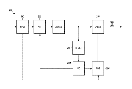
a polynomial
curve, an exponential curve, a logarithmic curve, or any other desired
response.
[0073] The amplifier 550 amplifies the RF signal that is passed through
from the RF
detector circuit 510. The amplified signal drives the laser 540. Preferably,
when amplifying the
RF signal from the RF detector 510, the laser bias control module 530 includes
a circuit that
modulates the amplifier gain to be proportional to the laser bias. This
effectively sets the gain of
the amplifier 550 to be proportional to the laser turn-on 560, and thereby
reducing or even
preventing over shoot and clipping by the laser 540. The laser's output is
then propagated from
the ONU on a fiber 570.
[0074] FIG. 11 shows the output of the laser 540 when using the system of
FIG10. As
seen in this figure, when using an RF gain factor proportional to the laser
bias, the clipping no
19
CA 02946395 2016-10-19
WO 2015/164036 PCT/US2015/023983
longer occurs. However, the variation in RF level during the laser turn-on may
potentially cause
an issue in the burst receiver that may expect a near constant RF level during
the laser turn-on.
To mitigate this, in some embodiments, the amplifier bias may be modulated to
delay the RF
signal to the laser, relative to the turn-on time of the laser 540, and may
also apply a faster time
constant than the optical power turn on. This embodiment is illustrated in
FIG. 12.
[0075] FIG. 13 shows an implementation of an ONU that includes a delay in
the RF
signal to the laser, relative to the turn-on time of the laser, and also
applies a faster time constant
than the optical power turn-on. Specifically, a novel ONU upstream
architecture 600 includes an
RF detector 610 that detects whether an RF signal is present at its input 620.
If a signal is
detected, the RF detector 610 passes the signal through to an amplifier 650
and also signals a
laser/amplifier bias control module 630 to turn on at time tO a laser 640,
which has a turn-on time
560. The laser/amplifier bias control module 630 preferably modulates the bias
of the laser 640
to achieve a full turn-on of the laser 640 over a turn-on time 660 that is
preferably as slow as
possible, e.g. the slowest turn-on time allowed by the RFoG standard, or in
some embodiments
even longer. In some embodiments, the turn-on time of the laser 640 could be
up to 500ns, lius,
or longer. This may greatly reduce the low frequency noise. The turn-on time
for the laser may
be linear, as shown in FIG. 13, or may implement a transition along any other
desired curve,
such as a polynomial curve, an exponential curve, a logarithmic curve, or any
other desired
response.
[0076] The amplifier 650 amplifies the RF signal that is passed through
from the RF
detector circuit 610. The amplified signal drives the laser 640. Preferably,
when amplifying the
RF signal from the RF detector 610, the laser/amplifier bias control module
630 includes a
circuit that modulates the amplifier gain to be proportional to the laser
bias, but with a delay 680
relative to the time to that the laser 640 begins to turn on. Preferably, the
rise time of the
amplifier gain is faster than the rise time of the laser turn-on. In some
embodiments, the
laser/amplifier bias control module 630 simply switches on the RF gain, i.e.
the rise time is as
short as the amplifier allows. The laser's output is then propagated from the
ONU on a fiber 670.
[0077] This ONU shown in FIG. 13 effectively sets the gain of the
amplifier 650 to be
proportional to the laser turn-on 560, and thereby reducing or even preventing
over shoot and
CA 02946395 2016-10-19
WO 2015/164036 PCT/US2015/023983
clipping by the laser 640, while at the same time mitigating problems caused
by a receiver
expecting a near-constant RF level during the time that the laser turns on.
The ability to
simultaneously reduce the laser turn-on time and to provide an RF gain to the
laser in proportion
to the laser turn-on time, but delayed with respect to the laser turn-on time
is a feature that has
great potential in all applications, and without loss of generality these
techniques may be used for
any analog application such as DOCISIS 3.0 or 3.1.
[0078] Either (or both) of the architectures shown in FIGS 10 and 13 may
be used
together with the architecture shown in FIG. 2 so as to further improve speed
and stability of
HFC systems. These may further be used together with the long term clipping
reduction
discussed in the previous disclosure to reduce the effects of both long term
and short term
clipping in the system.
[0079] Burst Detection
[0080] As indicated earlier, upstream transmissions typically operate in
burst-mode
(BM), where ONUs power up a transmitter, e.g. a laser, only during time
intervals when
information is to be transmitted along the upstream path. A burst-mode system
generally
provides a lower noise environment and thus enables better SNR, and in the
case the transmitter
is an optical device, the use of burst-mode tends to reduce Optical Beat
Interference (OBI).
Thus, in some preferred embodiments of the optical combiner system previously
disclosed in this
specification, where OBI is to be suppressed, such optical combiners are
preferably operated in
burst mode.
[0081] Also as indicated earlier, RFoG architectures that use burst-mode
detect the RF
level in the ONU, powering the ONU's laser when an RF signal is detected and
powering down
the laser when the RF signal is not present. This procedure is referred to as
"RF detection." In an
optical combiner, the optical light inputs coming from the ONUs are all
detected and the detector
outputs are collected. If RF detection is used with an optical combiner, an RF
comparator would
be applied to the output of the combined RF output. If the RF level output of
the combined RF
detectors were higher than the applied comparator, then the optical laser in
the optical combiner
would be activated.
21
CA 02946395 2016-10-19
WO 2015/164036 PCT/US2015/023983
[0082] However, such detection may be fraught with difficulties because
the RF level
input could be very small. For instance, a very small slice of a D3.1 signal
could be produced by
any single ONU, hence the modulation index of the ONU would be low, resulting
in a low RF
level at the optical combiner. Also, optical input power to the optical
combiner from a given
ONU could be low; with an optical input range spanning up to 12 dB, the RF
level after
detection could vary by 24 dB. As a result, the RF level from a photodiode
could still be so low
that the RF level that is to be detected would be lower than the comparator,
even if the RF level
were high relative to the Optical Modulation Index of the ONU laser that
generated the RF
signal. In ONU embodiments, the RF level could be turned on after the optical
output is turned
on, or while the optical output is being turned on, such that the detection of
an RF level at the
disclosed optical combiner would be delayed. Furthermore the detection could
also be slow,
because it depends upon the comparator circuit.
[0083] An alternative to using burst detection on the cascaded optical
combiner units
disclosed in the present application would be to keep the upstream light
transmission on all the
time, irrespective of whether signals are provided to the optical combiner or
not, i.e. an "always
on optical combiner". Though this would ensure that the optical combiner
transparently relays
information upstream, it would result in a constant light input at all the
ports at an upstream
optical combiner device or multiple port receiver. The total light input at
the ports thus could
lead to a summation of shot noise from all the ports, degrading the SNR
performance of the total
system. For this reason, in preferred embodiments, the optical combiner unit
transmits upstream
light only when an RF signal has been received and is to be sent out.
[0084] Disclosed herein is a novel method of burst detection that is
fast, simple, stable
and robust thus enabling multiple new architectures. Specifically, broadly
stated, the disclosed
optical combiner system may monitor the optical current of each photo diode as
well as the sum
current of all photodiodes. If any one of the photo diodes registers a photo
current, or
alternatively a current above a certain minimum value, the retransmitting
laser is automatically
turned on. The photodiode current generation is instantaneous and beneficially
is a DC value that
is easier to compare. As speeds of the interconnecting networks increase over
time, such optical
detection circuits will become more useful.
22
CA 02946395 2016-10-19
WO 2015/164036 PCT/US2015/023983
[0085] Such an Optical Burst Mode (OBM) detector promotes reliability and
may have
the following advantages: (1) in the case of multiple daisy chained optical
combiners as
disclosed in the present application, substantial reduction in the additive
shot noise is achieved
relative to an "always on" solution; (2) in the case of DOCSIS 3.1
transmission, individual signal
transmissions with very low RF levels per ONU may be detected and
retransmitted; and (3) in
the case of varying optical input levels due to different optical lengths
between the ONUs and the
disclosed active optical combiner, or varying optical lengths between multiple
daisy chained
such active optical combiners, reliable burst mode operation may still be
achieved.
[0086] Furthermore, the disclosed novel burst detection also enables
detection of light at
the input immediately at the start of a burst at the optical combiner input.
Conversely, where
there is no light at the input, or alternatively no light for a certain period
of time, the ancillary RF
amplifiers in the disclosed active optical combiner may be powered down, thus
reducing the
power dissipation of the disclosed active optical combiner. When light appears
at the input of the
disclosed active optical combiner, the amplifiers can be powered on again
within the time
allowed; for instance in an RFoG system up to one microsecond is allowed to
establish an optical
link from the moment that the RF input is detected and the system has started
to turn on. Because
RF amplifiers take a finite time to turn on and establish amplification; early
detection of a burst
is important to provide enough time to establish normal operation. Such power
cycling could
reduce power dissipation by as much as ten times, thus drastically improving
the critical
infrastructure metrics. Thus, for example in the event of a power outage, the
optical combiner
can conserve the power required by not only using optical burst operation, but
also circuitry for
RF burst operation, and extend a battery's life, if available.
[0087] Implementation of an optical power detection circuit capable of
covering a wide
range of optical input power, in an architecture having multiple detectors is
not trivial. Given the
large number of detectors present, combined with a wide optical input power
range, the amount
and range of photocurrent that needs to be reliably detected is considerable.
Simply measuring
the voltage drop across a resistor in the detector bias network is difficult;
at low input power on a
single detector, a small voltage drop can be reliably detected only if the
value of a resistor, across
which is a voltage drop equal to the photodetector bias, is relatively high.
However, increasing
the value of such a resistor is not desirable because this leads to an
increased voltage drop when
23
CA 02946395 2016-10-19
WO 2015/164036 PCT/US2015/023983
high detector currents are present at multiple detectors; the detector bias
would become a strong
function of the optical light present at the detectors. In some embodiments,
the detector bias is
held constant because detector responsivity depends on detector bias; thus a
varying the detector
bias could lead to a variation in the gain of the system. Even a resistance
value as low as a
typical transmission line impedance, such as 75 Ohms, can be problematic when
a large number
of detectors are active, and for instance 100 mA of detector current flows in
the multiple detector
system, leading to an excessive drop in detector bias.
[0088] Disclosed is a method to detect optical light over a wide input
power range while
retaining a constant bias on the detectors present in the transmission line
receiver. In order to
accomplish this, a combination of both an RF amplifier and a trans-impedance
amplifier are used
with the multiple detector structure. In some embodiments, the trans-impedance
amplifier is
connected to a high-pass structure in front of the RF amplifier such that for
low frequencies the
trans-impedance amplifier has a very low impedance connection (less than the
transmission line
impedance) to the detector bias.
[0089] Referring to FIG. 14, which shows an example of a transmission
line receiver
structure 700, a photo-detector may be accurately modeled up to fairly high
frequencies (¨ 1
GHz) by a capacitance in parallel with a current source for reasonable input
power levels (>1
uW). Thus, in this figure, each of the circuit elements 710 would be a model
of a photodetector.
Conventional receiver designs use a trans-impedance amplifier or match the
detector to as high
an impedance as possible, such as 300 Ohm, so as to convert the current source
signal to an RF
signal with the best possible noise performance. These approaches are limited
by the detector
capacitance such that an increase in the number of detectors by simply
combining detectors or
detector area leads to a loss of detector performance due to an increase in
combined detector
capacitance, and therefore a large number of detectors (e.g. 32) cannot
reasonably be expected to
work well with a single RF amplifier. This implies that multiple amplifiers
are needed to receive
a large number of fibers.
[0090] As an alternative. multiple detectors could be provided to an RF
combiner before
being amplified. An RF combiner requires that each detector be terminated
individually with an
RF impedance that is typically less than 100 Ohm, which will consume half of
the detector
24
CA 02946395 2016-10-19
WO 2015/164036 PCT/US2015/023983
current and, due to combining signals from multiple detectors, the RF combiner
will introduce an
additional loss of at least 10*log(N) dB, where N is the number of detectors
combined. This loss
becomes excessive for 8 detectors or more. Further, other losses are caused by
practical
implementations of RF combiners that require expensive transformers in their
realization. The
transformers also cause bandwidth limitations and aforementioned other losses,
and are difficult
to implement for high impedances (such as greater than 100 Ohm).
[0091] In the disclosed transmission line receiver, use is made of the
insight that a
reverse biased photo-detector behaves as a current source in parallel with a
capacitor with a low
loss at RF frequencies. This transmission line receiver will not induce the
10*log(N) loss of the
RF combiner, not require transformers, offer a high bandwidth and be able to
provide an output
signal representative of a delayed sum of a large number of detectors. A
transmission line with
impedance Z can be modeled by a ladder network of inductors and capacitors
with L/C=Z2,
which works well for frequencies under the resonance frequency of L and C.
Practical detector
capacitance values are on the order of 0.6 pF, such that a 75 Ohm transmission
line would
require L=3.4 nH. The resonance frequency is well over 1 GHz such that, for up
to 1 GHz, a
transmission line with an arbitrary number of detectors compensated with 3.4
nH inductors
would simulate a 75 Ohm transmission line. The quality of the parasitic
capacitance of the
reverse biased detectors is such that they can be considered low loss
capacitors at RF
frequencies. The 3.4 nH can also be distributed around the detectors as 2x1.7
nH, leading to a
design as shown in FIG. 14.
[0092] As indicated above, each current source/capacitor combination 710
represents a
detector. FIG. 14 shows a number of these in series, separated by respective
transmission line
sections 720 (100 psec or on the order of 1 cm on board) having 75 Ohm
impedance. The
detectors are matched with 1.7 nH inductors 730. A 75 Ohm resistor 740
terminates the input of
the transmission line. The output 750 of the transmission line feeds a low
noise 75 Ohm RF
amplifier (not shown). It should be understood that, although FIG. 14 shows
six detectors, there
is no limit on the number of detectors that can be combined by concatenating
these sections, and
up to the LC resonance frequency there is negligible impact on the attainable
bandwidth for a
large number of detectors. In practice the 1.7 nH inductors could be
implemented in the PCB
CA 02946395 2016-10-19
WO 2015/164036 PCT/US2015/023983
layout as narrower line sections, and a balanced transmission line with 100
Ohm or 150 Ohm
differential impedance may be used to slightly improve noise figure.
[0093] As shown in FIG. 14, each current source/capacitor combination 710
represents a
photo detector, where the current source is the detected current in the
detector; and the capacitor
represents the parasitic capacitance of the detector. Multiple detectors are
connected with
sections of transmission line (such as T2) and matching inductors (such as Ll
and L2). The
matching inductors are chosen such that the parasitic capacitance of the photo
detectors is
matched to the transmission line impedance (typically 75 Ohm). Thus, multiple
detectors can be
connected and concatenated to a transmission line, such that the detector
currents are provided to
the transmission line and these detector currents are equally divided to
propagate both to the
output 750 and to the termination resistor 740 at the other end of the
transmission line structure.
Each detector current generally passes through transmission line sections,
matching inductors,
and detector terminals before reaching an end of the transmission line. Thus,
signals from
adjacent detectors affect the signal voltages present at each detector
terminal and could therefore
affect the detector current itself, causing a cross-modulation of detector
signals. However,
because a detector at reverse bias can be modeled as a good current source,
such a cross-
modulation does not occur. Each detector current half is thus presented at the
output of the
transmission line as a signal with a delay proportional to the distance of the
detector to the output
of the transmission line. This distance determines the delay of an electrical
signal at the terminal
of the detector to the output of the transmission line and includes delay due
to matching
inductors and photo-detector capacitance. The signal at the output of the
transmission line is
therefore proportional to the sum of the delayed detector current halves,
independent of the
number of detectors in the transmission line structure. The signal at the
output of the
transmission line can thus be said to represent the sum of the delayed
detector currents.
[0094] The transmission line structure bandwidth is limited only by the
inductive
matching of the photo-diode capacitance and can be very large, exceeding 1
GHz. The output
750 is connected to an RF amplifier matched to the transmission line
impedance, which
amplifies the signals output from the transmission line structure. Note that
use of a trans-
impedance amplifier that is not matched to the transmission line structure
would cause a very
26
CA 02946395 2016-10-19
WO 2015/164036 PCT/US2015/023983
large reflection of the output signals back into the transmission line
structure; a trans-impedance
amplifier is not a preferable means to amplify the output from a transmission
line receiver.
[0095] Typically the photo detectors need to be biased, for instance with
5 V. In order to
decouple the bias voltage from the amplifier, a decoupling capacitor may
typically be used. The
bias can then be provided via an inductor in a bias-tee arrangement as shown
in FIG. 15, for
example. The signal from the transmission line 760 is provided to an amplifier
(not shown) via a
capacitor (770) that passes high frequency signals, and bias from a voltage
source 775 is
provided to the transmission line via an inductor 780 that passes low
frequency signals. The
termination resistor 740 at the other end of the transmission line is thus
capacitively decoupled to
permit a DC bias. The current through voltage source 775 can be measured to
determine
photocurrent; the voltage source 775 could be constructed as a trans-impedance
amplifier
providing a constant voltage and an output proportional to the current
provided. However, in
implementations, the inductor 780 needs to be chosen with a value large enough
that it does not
affect the low frequency response of the amplifier. As a consequence, there
may be a delay in the
response of the current in the inductor 780 to a change in photo detector
current, and this tends to
cause a delay in the detection of photocurrent.
[0096] FIG. 16 shows an implementation 800 that uses both ends of the
transmission line
receiver structure to alleviate such a delay. The resistor R1 in FIG. 16 is
the termination resistor
740 shown in FIG. 14, and the inductor Ll is the inductor 780 in FIG. 15. The
voltage source
810 provides bias both to the termination resistor 740 and the inductor 780.
The current in
resistor 740 responds instantly to a photocurrent such that a fast detection
of photocurrent is
enabled. The inductor 780 can support large photocurrents without a
significant voltage drop
such that large photo currents can be supported without a significant drop in
bias to the photo
detectors. A capacitance 815 can be placed adjacent to the voltage source 810;
for an ideal
voltage source it may not carry any current because the voltage is constant.
However at RF
frequencies it can be difficult to realize a perfect voltage source, hence the
capacitor 815
provides a low impedance to ground such that RF currents in the termination
resistor 740 do not
cause modulation of the voltage at the voltage source 810.
27
CA 02946395 2016-10-19
WO 2015/164036 PCT/US2015/023983
[0097] In order to realize an efficient detection circuit for the current
in voltage source
810, the voltage source 810 is preferably implemented as a trans-impedance
amplifier. A trans-
impedance amplifier is a basic electronic circuit that holds a node between
two current paths at a
constant voltage and has an output that changes its output voltage in
proportion to the current
provided at that node. Thus, externally the trans-impedance amplifier looks
like a voltage source
to that node, but there is an additional output that represents the current
provided. This output
may then be used to drive a decision circuit to decide if a photo-current
flows or not. Due to the
fact that the trans-impedance amplifier is realized with a practical
transistor circuit, it does not
have infinite bandwidth, which means that it is not able to hold the node
voltage constant for
very high frequencies and for that reason the capacitor 815 may be added in
some embodiments.
[0098] It should be understood that in some embodiments, the LC bias
network prior to
the amplifier (capacitor 770 and inductor 780) may be replaced by more complex
circuits, or
even with diplex filters - provided that the network provides a low-loss, high-
frequency path
from the transmission line detector to the amplifier, and a low-loss (low
impedance) path at low
frequency from the voltage source (trans-impedance amplifier) to the
transmission line detector
bias. It should also be noted that the trans-impedance amplifier may be
implemented such that
the output voltage first changes linearly as a function of photo-current, but
then saturates at a
photo-current that is sufficiently high.
[0099] In other implementations, a photocurrent detection circuit may be
applied to each
individual photo detector; optionally one electrode of a photo detector (for
instance cathode) may
be connected to an RF circuit and the other electrode (for instance anode) may
be connected to
an optical power detection circuit. This increases complexity, as a detection
circuit is required
per detector. Also, some embodiments may optionally use a trans-impedance
amplifier per
detector.
[00100] With an optical burst mode detection circuit, for instance of the
type described
above, the bias of a laser or the bias or gain of an amplifier may be
controlled. FIG. 17 shows a
multiple-detector receiver 820 that produces an output 825 signaling that
power has been
detected from any one of multiple inputs 830. This detection can be based on a
detection method
as described in the previous section or on multiple detector circuits that are
monitoring individual
28
CA 02946395 2016-10-19
WO 2015/164036 PCT/US2015/023983
detectors 835. When optical input has been detected at time tO then the laser
bias is turned on
with a controlled rise time t on 1 and the active combiner can re-transmit
signals present at the
inputs.
[00101] The optical burst mode detection can further be used to control
the amplifier bias
as shown in FIG. 18; when optical power is detected at tO the amplifiers are
immediately turned
on. The laser turns on more slowly such that the amplifiers are settled by the
time that the optical
power is on. Optionally this scheme may be expanded by a third control signal
850 that controls
the amplifier gain, as shown in FIG. 19.
[00102] Optical Modulation Index and Self Calibration
[00103] For implementations that permit operation of all upstream inputs
of the active
splitter simultaneously, the total amount of photocurrent on the detectors
following the upstream
inputs can be high. The impedance of the bias circuit and, as discussed, of
the aforementioned
filtering means in the detector output path must be low.
[00104] In an existing RFoG system, the CMTS controls the output level of
the cable
modems' communications with ONUs that are transmitting RF signals to a head
end such that a
desired input level to the CMTS is obtained. This implies that the output
level from a receiver
preceding the CMTS is adjusted to a known level. If this receiver is of a type
that has a known
amount of gain such that an output level corresponds to a known optical
modulation index, then
this implies that the optical modulation index of channels provided to the
CMTS is known -
given the RF signal level to which the CMTS adjusts the channel. This requires
a calibrated
receiver that adjusts its gain as a function of the optical input level (2 dB
gain increase for every
dB reduction in optical input level) such that this fixed relation between RF
output level and
optical input level is maintained. The modulation index into the receiver is
the modulation index
of the upstream laser in the active splitter connected to that receiver; thus
the CMTS implicitly
controls the modulation index of that active splitter output.
[00105] The gain of the active splitter should preferably be set such that
an output
modulation index from that active splitter has a known relation to an input
modulation index at
one or more of the photo detectors receiving upstream signals from active
splitters or ONUs
29
CA 02946395 2016-10-19
WO 2015/164036 PCT/US2015/023983
further downstream. This requires knowledge of the photocurrents at these
photo detectors, and
preferably the active splitter can monitor the photo current of each upstream
liffl( by using one
detector per upstream link as in a transmission line detector, for instance.
Since some systems
may operate in burst mode, these photo currents are not always available.
However, in a
DOCSIS system all ONUs are polled repeatedly to obtain an acknowledgement
signal with an
interval up to five minutes. This implies that upstream active splitters are
re-transmitting the
information, and all active splitters in such a system have each one of the
upstream inputs active
at least once every five minutes. The active splitter can thus record the
burst levels and build a
map of optical input levels to input ports. Using this information, the active
splitter can set an
internal gain level such that the upstream modulation index is maximized, but
will not clip so
long as the input signals to the active splitter are not clipping. Whereas the
fiber length from
head end to first active splitter is generally long, those fiber lengths
between active splitters and
those fiber lengths from active splitters to ONUs are generally short, and
have small enough loss
that the optical input power values to the different upstream input ports are
close, and the optimal
gain setting is similar for all ports. As a consequence, the optimal gain
setting in the active
splitter is almost the same for all input ports and the compromise in SNR from
assuming a worst
case reverse laser modulation index from a signal on any of the input ports is
small.
[00106] As noted earlier, one embodiment could use the high and low
optical output
power setting for the reverse laser, instead of switching the laser between a
high output power
for burst transmission and an off state in between. Not only does this
embodiment provide
continuous information to active splitters about the link loss to the ONU, it
also improves laser
operation. When a laser powers on, the transient leads to a brief transition
where laser distortion
is high and RF input signals can be clipped. If a laser is held at a low power
level instead of
being in the off state before being turned on to a higher power level, then
this transient is near
absent and distortions and clipping are reduced. In case the laser is held at
a high output power
continuously, these transients and distortions are absent. The active splitter
architecture permits
operating the ONUs in any of these three modes and an optimum can be selected
for system
operation.
[00107] Whereas the upstream input power levels to detectors on an active
splitter are
typically similar, in some instances they may differ due to differences in
connector loss or fiber
CA 02946395 2016-10-19
WO 2015/164036 PCT/US2015/023983
loss. Preferably, all optical inputs would have the same level or have the
same RF level
following the detector for an equivalent channel load. Since the active
splitter can monitor the
power level at each detector and map those optical input levels, it can
compute adjustments to
optical input power level or in modulation index of those inputs that would be
required to
equalize the RF levels following the detectors of each input. The active
splitter can communicate
those preferred settings for output power level or gain for the reverse
transmitters downstream
that are connected to the inputs. The communication signals can be modulated
onto a laser
injected into the downstream signals or onto pump laser currents in EDFAs
amplifying
downstream signals. The modulation can be selected to be small enough, and in
such a frequency
band, that the communication signals do not interfere with the downstream
payload.
[00108] Preferably, not only active splitters receive and interpret these
communication
signals, but also downstream ONU units receive and interpret the signals. This
would permit
essentially perfect alignment of the optical transmission level and RF gain of
all units in an
active splitter system. Given the presence of an upstream laser, and the
ability of all components
in an active splitter system to receive an upstream signal, all components in
an active splitter
system are capable of upstream communication with the addition of a simple
tone modulation or
other scheme. Thus, bidirectional communication is enabled, and active
splitters and the head
end can communicate with each other, self-discover the system, and setup
optimal gain and
optical levels.
[00109] One objective of the active splitter architecture is to provide
accurate RF levels to
the CMTS that represent an optical modulation index. Doing so is not trivial,
and requires a
specific self-calibration procedure (later described) that is expected to
result in accurate
modulation index correlation to active splitter head end receiver output RF
levels. The receiver is
either a CMTS plug-in or is connected directly to the CMTS without unknown RF
loss
contributions in between (in case a tap is needed for other services than the
CMTS, the tap can
be integrated in the receiver to avoid external RF losses). As a consequence,
the modulation
index of the active splitter re-transmitter units is set precisely.
[00110] In case bidirectional communication is not available then the ONU
output power
level cannot be adjusted by the active splitter and the modulation index of
the ONU will still
31
CA 02946395 2016-10-19
WO 2015/164036 PCT/US2015/023983
have some uncertainty since the optical loss between ONU and the active
splitter/receiver can
vary; a +/- ldB loss variation from ONU to active splitter would result in a
+/- 2 dB tolerance in
RF level, thus a dynamic window will at least have to accommodate that
variance and headroom
for other tolerances and CMTS setup accuracy. This should be readily available
for bandwidths
up to 200 MHz such that even without the active splitter controlling the ONU's
output power,
acceptable system performance can be obtained. With the aforementioned
bidirectional control
additional system headroom can be achieved.
[00111] When 1200 MHz return bandwidth is used, such that ONUs are
assigned 200
MHz widths of spectrum, the ONUs can all be operated a few dB below their clip
point, i.e. just
enough to cover the uncertainty in the loss from the ONU to the active
splitter to avoid clipping
of the ONUs. This optimizes the performance of the critical liffl( from the
ONU to the active
splitter, so that 0 dBm ONUs are sufficient. In this type of operation, an
arbitrary choice can be
made for the number of ONUs operating with such a 200 MHz band, for instance
up to six
ONUs. This in turn would cause clipping in the active splitter transmitter;
thus for 1200 MHz
operation, the gain of the active splitter receivers following the ONUs can be
reduced by 8 dB
such that when six ONUs are transmitting 200 MHz of signal bandwidth, the
active splitter
reverse transmitter is operated just below clipping. This method of operation
maximizes SNR
and eliminates uncertainty - the impact of variance in the link between the
ONU to the active
splitter is minimized, and the active splitter links are operated with a
precise modulation index as
with lower bandwidth RF return systems. The required dynamic window is reduced
to tolerances
in CMTS level setting and active splitter output level calibration, permitting
operation at an
optimal modulation index.
[00112] Analysis of the attainable SNR using the system just described,
for 1200 MHz
operation with a maximum load of 200 MHz per ONU, results in a 5 dB
improvement in the
SNR attainable at 1200 MHz. This results in about 20% more throughput capacity
in the system.
With 1200 MHz of bandwidth, the total upstream data rate could be as high as
10 Gbs.
[00113] In case the system is initially set up so that the active splitter
units expect a 1200
MHz return spectrum (instead of for instance 200 MHz) with a maximum of 200
MHz per ONU,
then a penalty of around 7 dB occurs in terms of peak NPR performance.
Therefore, the mode of
32
CA 02946395 2016-10-19
WO 2015/164036 PCT/US2015/023983
operation preferably can be switched between normal operation, where a single
ONU can occupy
the entire spectrum, and high bandwidth operation where a single ONU can be
assigned a limited
amount of spectrum at any time and the active splitter reverse transmitters
support the entire
spectrum at once.
[00114] The proposed architecture has multiple re-transmission links that
are preferably
operated at the best possible modulation index on the assumption of perfect
alignment of the
NPR (Noise Power Ratio) curves of those links. As noted earlier, the alignment
of the re-
transmission in the active splitter return links is critical to obtain the
best possible performance
(every dB of mis-alignment directly results in a reduction of available SNR)
hence a calibration
technique is needed to set and hold the correct alignment of transmitter gain
factors.
[00115] In order to provide such calibration, the active splitter return
transmitter gain will
be set accurately, such that for a given detector current of the active
splitter receiver diodes, the
modulation index of the transmitter is equal to the modulation index input to
the detector. This
only requires knowledge of the detector current; the actual optical input
power to the detector
and the detector responsivity are irrelevant. In order to accomplish this,
means are implemented
at each detector to measure detector current such that an appropriate gain can
be set for the return
transmitter.
[00116] The gain may be set individually for each detector, but since
multiple detectors
can be receiving signals at the same time, this would require a controllable
attenuator for every
detector (32 detectors are in a typical active splitter unit). Preferably, a
single attenuator is used
for all detectors. This is achieved using variable output transmitters in the
active splitter units,
communicating to an upstream active splitter or variable output transmitters
in ONUs
communicating to an upstream active splitter. Outlined below is a method to
set the output level
of each of the reverse transmitters such that each transmitter provides the
same photocurrent on
the detector to which it is coupled. During normal operation, the active
splitter receiver monitors
the detector currents during bursts to enable issuance of a warning in case an
optical link
degrades or is lost.
[00117] For a 1310 nm reverse link from the active splitter to an upstream
active splitter,
the reverse laser power typically needs to be controlled from either 3-10 dBm
or 6-10 dBm,
33
CA 02946395 2016-10-19
WO 2015/164036 PCT/US2015/023983
depending on the design of the active splitter receiver. For a 1610 nm reverse
link, these figures
are typically 3-7 dBm or 6-7 dBm, respectively. These controls ensure that the
power received at
the end of a 25 km link, with some WDM loss, is at least 0 dBm. It should be
understood that the
numbers given are examples. The active splitter can transmit information in
the forward direction
through pump modulation of the EDFA or injection of a signal into the forward
path. The latter
is more expensive; the former results in a lower data rate, as only a minimal
pump fluctuation
can be allowed without affecting the forward path. A low data rate is
sufficient, and can be read
by a simple receiver - for instance a remote controller receiver operating in
the kHz range
coupled to a low cost processor. It should be understood that the downstream
transmit function is
only required in upstream active splitter units unless ONUs are being
controlled as well. In the
figures shown, that would be one out of 33 active splitter units in the
system.
[00118] In a self-calibration run, the upstream active splitter unit
transmits a command
downstream to active splitter units to initiate self-calibration. Subsequently
the downstream units
randomly turn their transmitters on and off at full power with a low duty
cycle, such that in
nearly all cases at most one of the downstream units is on. The upstream
active splitter reports
information downstream as to which port is on, and what detector current it
has obtained from
that unit. The downstream units record that information in non-volatile
memory; since it can
correlate the messages to its own activity, this provides information to the
downstream unit as to
what port it is on and what power it provided to that port. After all ports
have been on at least
once, or a time out has occurred (for instance if one or more ports are not
connected), the
upstream active splitter unit determines which downstream active splitter
produces the smallest
detector current. Next, the upstream active splitter computes how the upstream
powers of each of
the downstream units should be set, such that all detector currents are the
same and fall within a
specified range. That range can for instance correspond to 0-3 dBm (or 6 dBm)
input power at
the detectors. It should be understood that this can be accomplished by
setting a photodetector
current, and does not require measurement of an exact optical input power.
[00119] Generally, the active splitter upstream unit will set this power
to the best (or
maximum) value that can be obtained to optimize the SNR of the links. The
active splitter units
will then all have a known output power, and their internal gain will
accordingly be set to have a
calibrated modulation index for a given input power and modulation index. All
links into an
34
CA 02946395 2016-10-19
WO 2015/164036 PCT/US2015/023983
upstream active splitter may behave identically. The upstream active splitter
unit may then take
the downstream units out of calibration mode.
[00120] In case an additional port is lit up on an upstream active
splitter receiver port, then
the self-calibration algorithm can proceed without service interruption of
already connected
active splitter units. This is achieved by activating self-calibration on the
downstream active
splitter receiver that has just been activated by requesting calibration mode
only for units with
unknown port number (that is only the new unit). Its output will turn on and
the upstream active
splitter unit will then assign a port number to the new, hitherto unused port
and set a power to the
new unit, and take it out of calibration mode.
[00121] During normal operation, the upstream active splitter unit
continues to monitor
receiver currents for the incoming upstream links. If there is significant
deviation, it may still
issue a non-calibration mode downstream command to re-adjust power, and it can
also signal
plant issues upstream.
[00122] The active splitter units operated in the disclosed manner can
also build a map of
connected active splitter units. Also, a map can be created of upstream power
from connected
ONUs and statistics on individual ONU operation and liffl( loss can be
collected, for instance to
locate chattering ONUs or poor ONU connections.
[00123] The head end transmitter can also send a command to downstream
active splitter
units to initiate calibration or change a mode of operation (for instance from
200 MHz to 1200
MHz optimized operation). Any other type of bidirectional EMS system
monitoring can be
envisioned for active splitter units that can receive and transmit low data
rate traffic. It should be
understood that this does not require complex or costly HFC EMS systems; minor
optical power
fluctuations by either pump power variation or low level signal injection in
the downstream
signal path, or reverse laser power variation in the upstream path, are
sufficient to detect binary
or kHz range (like remote control chips) modulated data patterns. It should
also be understood
that the most expensive option - injection of a downstream optical signal - is
only relevant at the
head end, or in the upstream path typically only relevant in 1 out of 33
active splitter locations.
CA 02946395 2016-10-19
WO 2015/164036 PCT/US2015/023983
[00124] Another important consideration is that the CMTS should set up
modem levels
correctly. In regular return or RFoG systems, there is considerable
uncertainty in system levels
due to RF components or applied combiner networks. In the active splitter
system, however,
there are no RF components in the link, the service group is aggregated in the
optical domain,
and only one low gain, low performance, and low output level receiver is
required which is
coupled directly to the CMTS return port. In some embodiments, it may be
desirable to produce
a dedicated active splitter receiver with an accurately calibrated output
level as a function of
input modulation index. Such a receiver has no need for a wide input range; -3
to +3 (or 0 to +6)
dBm is sufficient. The high input level implies that the gain can be low. The
absence of RF
combining following the receiver also means that the output level can be low.
Therefore, such a
receiver should be obtainable in a high density, low power form factor. With
such a receiver,
little if any RF wiring may be required in the head end, and the CMTS can
accurately set reverse
levels to obtain the correct optical modulation index. In some cases, there
may be a need to
connect other equipment than the CMTS to the reverse path. The receiver may
use an auxiliary
output to provide for this functionality, rather than the main output with
external RF splitters.
This eliminates any level uncertainty due to RF components between the
receiver and the CMTS.
[00125] Embodiments
[00126] Some embodiments of the foregoing disclosure may encompass
multiple cascaded
active splitters that are configured to work with ONUs based primarily on
optical input levels
without requiring bidirectional communication. Other embodiments may encompass
multiple
cascaded active splitters that are configured to work with ONUs by using
bidirectional
communication.
[00127] Some embodiments of the foregoing disclosure may include an active
splitter with
multiple optical inputs, each providing an optical input to one or more
detectors that together
output a combined signal to a high pass filter that presents a low impedance
to the detectors and
rejects all signals below an RF frequency band and passes all signals above an
RF frequency
band before presenting the combined signal to an amplifier and a re-
transmitting laser.
[00128] Some embodiments of the foregoing disclosure may include an active
splitter with
multiple optical inputs, each providing an optical input to one or more
detectors that together
36
CA 02946395 2016-10-19
WO 2015/164036 PCT/US2015/023983
output a combined signal, where the active splitter has a bias circuit with a
sufficiently low
impedance at low frequency such that all detectors can be illuminated at the
same time without a
significant drop in bias to the detectors.
[00129] Some embodiments of the foregoing disclosure may include an active
splitter with
a reverse laser where the reverse laser turns on when a photocurrent at the
active splitter input
detectors is above a threshold, and where the slew rate when the laser turns
on is limited such
that it does not create a transient having a spectrum that interferes with the
upstream spectrum to
be transmitted.
[00130] Some embodiments of the foregoing disclosure may include an RFoG
active
splitter architecture where reverse lasers of the active splitter(s) and /or
ONUs connected to the
active splitter(s) are operated with a continuous output. Some embodiments of
the foregoing
disclosure may include an RFoG active splitter architecture where reverse
lasers of the active
splitter(s) and /or ONUs connected to the active splitter(s) are operated
between a high and a low
power mode such that the output power is high during bursts of upstream
transmission and is
otherwise low in output. Some embodiments of the foregoing disclosure may
include an RFoG
active splitter architecture where reverse lasers of the active splitter(s)
and /or ONUs connected
to the active splitter(s) may be selectively set to either one of a continuous
mode and a burst
mode.
[00131] Some embodiments of the foregoing disclosure may include an RFoG
ONU that
switches between a high and a low output power state where the output power is
high during
burst transmission of information and where the low output power state is
above the laser
threshold.
[00132] Some embodiments of the foregoing disclosure may include an RFoG
system that
measures detector currents at all inputs, building a table of detector
currents during high and low
(or no) input power to the optical inputs and computes, based on that table, a
gain value such that
a modulation index of the reverse transmitting laser has a known relation to a
modulation index
at the optical inputs to the active splitter, such that the reverse
transmitting laser has an optimal
modulation index but clipping is prevented, even for the port with the highest
optical input. In
37
CA 02946395 2016-10-19
WO 2015/164036 PCT/US2015/023983
some embodiments of the foregoing disclosure, the optimal modulation index of
the reverse
transmitter is nominally the same as that for the optical inputs.
[00133] Some embodiments of the foregoing disclosure may include an RFoG
ONU with
an RF signal detector that detects bursts of input signals and activates a
laser at a high power
mode when a burst is detected and otherwise activates the laser at a low power
mode, such as
zero power. An electrical attenuator may precede the laser driver and may
attenuate an RF input
signal, such that in the low output power state the laser cannot be clipped by
an RF input signal.
The RF attenuation before the laser may be reduced as the laser power
increases from the low
power state, such that the RF attenuation is rapidly removed to have minimal
impact on the burst
but during the transition, the laser still is not clipped.
[00134] Some embodiments of the foregoing disclosure may include an RFoG
ONU with
an RF signal detector that detects bursts of input signals and includes an
electrical attenuator that
precedes the laser driver to attenuate the RF input signal, such that when no
nominal input is
present noise funneling by the ONU of weak noise signals into the ONU is
prevented and RF
attenuation is rapidly removed when a burst is detected to have minimal impact
on the burst.
[00135] Some embodiments of the foregoing disclosure may include an RFoG
ONU that
can receive a downstream signal instructing it to adjust output power level,
RF gain or both. In
some embodiments, such an ONU can receive assigned port numbers and status
monitoring
requests. In some embodiments, such an ONU can transmit upstream information
such as status,
serial number, etc.
[00136] Some embodiments of the foregoing disclosure may include an active
splitter that
can transmit a downstream signal with requests to downstream units to adjust
optical power
level, gain or to request status information. Some embodiments may include an
active splitter
that can receive such downstream signals. Some embodiments may include an
active splitter that
can transmit and/or receiver such signals in the upstream direction, as well.
[00137] Some embodiments of the foregoing disclosure may include an ONU
with an RF
detector, an attenuator, a bias circuit, and a microcontroller where the
microcontroller estimates
laser clipping based on measured RF power levels and tracks what fraction of
the time the laser
38
CA 02946395 2016-10-19
WO 2015/164036 PCT/US2015/023983
is clipping and increases attenuation in case this fraction exceeds a
threshold. The
microcontroller may also adjust laser bias to prevent clipping. In some
embodiments, the
microcontroller brings attenuation to a nominal value when RF power to the
laser is at or below a
nominal value. In some embodiments, changes in attenuation made by the
microcontroller take
place in discrete steps in time and magnitude.
[00138] In some embodiments of the foregoing disclosure the
microcontroller may set the
attenuation to a high enough level to prevent clipping but less than needed to
obtain a nominal
modulation index.
[00139] Some embodiments of the foregoing disclosure may include a
bidirectional RF-
over-fiber architecture with more than one re-transmission liffl( in the
reverse direction, where
detected signals from preceding links are combined at each re-transmission
link.
[00140] Some embodiments of the foregoing disclosure may include a
calibrated receiver
at a head-end that provides a specific RF output level for an input modulation
index, with a gain
control such that for different optical input levels, the RF output level for
a given modulation
index is held constant. In some embodiments, a receiver may include two
outputs, at least one
connected to a CMTS without any RF combining and splitting networks.
[00141] Some embodiments of the foregoing disclosure may include an active
splitter with
at least two gain settings, one gain setting optimized for ONUs that can
transmit the full reverse
spectrum that the system can support, and one setting optimized for ONUs that
can transmit an
amount of spectrum less than the full spectrum that the system can support,
where the active
splitter combines inputs from multiple ONUs and can transmit the full spectrum
that the system
can support.
[00142] Some embodiments of the foregoing disclosure may include an active
splitter
having adjustable reverse transmission power and adjustable gain such that,
for a given received
upstream signal modulation index, the active splitter maintains a constant
optical modulation
index irrespective of optical output power. In some embodiments, the
retransmitted optical
modulation index is the same as the received optical modulation index. In some
embodiments,
39
CA 02946395 2016-10-19
WO 2015/164036 PCT/US2015/023983
the retransmitted optical modulation index is a predetermined fraction of the
received optical
modulation index, and the splitter enables an option to vary that fraction.
[00143] Some embodiments of the foregoing disclosure may include an active
splitter that
can receive and decode forward communication signals, e.g. an input-monitoring
diode for an
EDFA, or another monitoring diode.
[00144] Some embodiments of the foregoing disclosure may include an active
splitter that
can transmit forward communication signals, with for instance a forward laser,
or by modulating
the pump current of an EDFA.
[00145] Some embodiments of the foregoing disclosure may include an active
splitter that
can receive and decode upstream communication signals, e.g. by monitoring
upstream detector
currents. Some embodiments of the foregoing disclosure may include an active
splitter that can
transmit upstream communication signals, e.g. by modulating the reverse laser.
[00146] Some embodiments of the foregoing disclosure may include a system
with at least
two active splitters where a first active splitter instructs a second active
splitter to adjust its
reverse transmission power level. Some embodiments may use an algorithm to
equalize and
optimize the reverse transmit level of all downstream active splitters
connected to an upstream
active splitter. In some embodiments, the algorithm is executed automatically
at start up such
that downstream active splitters (and optionally ONUs) obtain an address and
optionally report
in the upstream direction the splitter' s (or ONU's) serial number and status.
In some
embodiments, later activation of ports in the splitter leads to an automatic
calibration of new
ports without interrupting the service of existing ports, and with continuous
monitoring of port
health.
[00147] Some embodiments of the foregoing disclosure may include an active
splitter
capable of upstream communication, and capable of receiving and decoding
upstream
communications from another splitter.
[00148] In some embodiments, an active splitter may establish a map of the
system in
which it is included, and may report system status and topology information to
a headend and
may issue alarms if necessary. The map may include serial numbers of active
splitters, and may
CA 02946395 2016-10-19
WO 2015/164036 PCT/US2015/023983
include serial numbers of connected ONUs. Some embodiments may create a system
map
automatically, and (i) may monitor ONU liffl( input levels to active
splitters; (ii) may detect
chattering or otherwise defective ONUs and optionally instruct active splitter
to shut down
detectors of defective or chattering ONUs; and/or (iii) may monitor the status
of the active
splitter that construct the map. In some embodiments, the monitoring function
is used to
automatically trigger route redundancy by monitoring upstream traffic on a
link, to determine if
the liffl( is intact, and if the liffl( is found to be defective, switching
downstream traffic to an
alternate upstream link. In some embodiments, upstream active splitters
monitor downstream
active splitters by communicating with downstream active splitters.
[00149] Some embodiments of the foregoing disclosure may include a head
end that
instructs downstream active splitters to initiate a self- calibration
procedure.
[00150] Some embodiments include a combiner that can monitor each of the
upstream
input ports and thus detect a loss of a link to such a port. The loss of an
upstream link implies
that the associated downstream link has been lost. Detection of a link can be
used to initiate
switching over to a redundant fiber link, preferably following a different
fiber route.
[00151] The terms and expressions that have been employed in the foregoing
specification
are used therein as terms of description and not of limitation, and there is
no intention, in the use
of such terms and expressions, of excluding equivalents of the features shown
and described or
portions thereof, it being recognized that the scope of the claimed subject
matter is defined and
limited only by the claims that follow.
41