Note: Descriptions are shown in the official language in which they were submitted.
1
WO 2015/177988 PCT/JP2015/002423
Description
Title of Invention: CIRCUIT BOARD POWER STORAGE
DEVICE, BATTERY PACK, AND ELECTRONIC DEVICE
CROSS REFERENCE TO RELATED APPLICATIONS
[0001] This application claims the benefit of Japanese Priority Patent
Application JP
2014-105963 filed May 22. 2014, and Japanese Priority Patent Application JP
2015-002590 tiled January 8, 2015
Technical Field
[0002] The present technology relates to a circuit board, a power storage
device, a battery
pack, and an electronic device.
Background Art
[0003] A circuit board in which a component such as an integrated circuit
or a resistor and a
wiring of a conductor such as thin and narrow copper come in close contact
with each
other on an insulating base material by being bonded through solder bonding is
built in
an electronic device. Technologies related to the circuit board are described
in PTL 1
and PTL 2.
Citation List
Patent Literature
[0004] PTL 1: Japanese Unexamined Patent Application Publication No. 2003-
318332
PTI, 2: Japanese Unexamined Patent Application Publication No. 2013-175590
Summary
Technical Problem
[0005] In the circuit board, long-term reliability of the solder bonding
has to be improved.
[0006] It is desirable to provide a circuit board capable of improving long-
term reliability of
solder bonding, and a power storage device, a battery pack and an electronic
device
that include the same.
Solution to Problem
[0007] In one embodiment, an electronic apparatus is provided including a
substrate, a
conductive land formed on a surface of the substrate, an electronic component
including an electrode, at least one insulating protrusion formed on the land
in an
overlapping region between the land and the electrode in plan view, and a
solder that
bonds the electronic component to the land, the solder being formed between
the
electrode and the land in the overlapping region in a normal direction to the
surface of
the substrate.
CA 2947519 2019-07-08
2
CA 02947519 2016-10-31
WO 2015/177988 PCT/JP2015/002423
[0008] In another embodiment, an electronic apparatus includes a substrate,
a conductive
land formed on a surface of the substrate, the land including a cut out
portion that
exposes a portion of the underlying substrate, an electronic component
including an
electrode, and a solder that bonds the electronic component to the land. In
this em-
bodiment, the solder is formed between the electrode and the substrate in the
cut out
portion of the land in a normal direction to the surface of the substrate.
Also, at least
part of the cutout portion is in an overlapping region between the land and
the
electrode in plan view.
[0009] In another embodiment, an electronic apparatus includes a substrate,
a conductive
land formed on a surface of the substrate, an electrode or a terminal
electrically
connecting an electronic component, at least one insulating protrusion formed
on the
land in an overlapping region between the land and the electrode in plan view,
and a
solder that bonds the electrode or the terminal to the land, the solder being
formed
therebetween.
100101 In another embodiment, an electronic apparatus includes a substrate,
a conductive
land formed on a surface of the substrate, the land including a cut out
portion or a dent,
an electrode or a terminal electrically connecting an electronic component,
and a solder
that bonds the electronic component to the land, the solder being formed
therebetween
in the cut out portion or the dent of the land in a normal direction to the
surface of the
substrate.
Advantageous Effects of Invention
100111 According to the embodiments of the present technology, it is
possible to improve
long-term reliability of solder bonding.
Brief Description of Drawings
100121 [fig.1A[Fig. 1A is a schematic plan view showing the configuration
example according
to a first embodiment of the present technology.
[fig.1B1Fig. 1B is a schematic cross-sectional view taken along line IB-IB of
Fig. 1A.
[fig.2A]Fig. 2A is a schematic plan view showing a modification example of a
shape
of a front end of a land.
[fig.2B1Fig. 2B is a schematic plan view showing a modification example of the
shape
of the front end of the land.
[fig.3A[Fig. 3A is a schematic plan view showing a positional relationship
between an
electrode and the front end of the land.
[fig.3B]Fig. 3B is a schematic plan view showing a positional relationship
between the
electrode and the front end of the land.
[fig.3C1Fig. 3C is a schematic plan view showing a positional relationship
between the
electrode and the front end of the land.
3
CA 02947519 2016-10-31
WO 2015/177988 PCT/JP2015/002423
Ifig.4A1Fig. 4A is a schematic plan view showing the configuration example of
a first
example of the circuit board according to the first embodiment of the present
technology.
[fig.4B1Fig. 4B is a schematic cross-sectional view taken along line IVB-IVB
of Fig.
4A.
Ifig.4C1Fig. 4C is a schematic cross-sectional view taken along line IVC-IVC
of Fig.
4A.
Ifig.51Fi2. 5 is a schematic cross-sectional view showing a modification
example of the
arrangement of a silk layer.
Ifig.6AlFig. 6A is a schematic plan view showing the configuration example of
a
second example of the circuit board according to the first embodiment of the
present
technology.
Ifig.6B1Fig. 6B is a schematic cross-sectional view taken along line VIB-VIB
of Fig.
6A.
Ifig.6C1Fig. 6C is a schematic cross-sectional view taken along line V1C-VIC
of Fig.
6A.
Ifig.71Fig. 7 is a schematic diagram showing the list of sizes of a typical
electronic
component and the list of dimension values of an electrode of each electronic
component.
Ifig.8A1Fig. 8A is a schematic cross-sectional view showing a part of the
circuit board.
[fig.8B1Fig. 8B is a schematic plan view showing a part of the circuit board.
Ifig.9AlFig. 9A is a schematic plan view showing a configuration example of a
circuit
board according to a second embodiment of the present technology.
1fig.9B1Fig. 9B is a schematic cross-sectional view taken along line IXB-IXB
of Fig.
9A.
[fig.10A1Fig. 10A is a schematic plan view showing the configuration example
of the
circuit board according to the second embodiment of the present technology.
[fig.10B1Fig. 10B is a schematic cross-sectional view taken along line XB-XB
of Fig.
10A.
[fig.11A1Fig. 11A is a schematic plan view showing a configuration example of
a
circuit board according to a third embodiment of the present technology.
[fig.1 I Wig. 11B is a schematic cross-sectional view taken along line XIB-XIB
of
Fig. 11A.
1fig.11C1Fig. 11C is a schematic cross-sectional view taken along line XIC-XIC
of
Fig. 11A.
Ifig.12AlFig. 12A is a schematic plan view showing the configuration example
of the
circuit board according to the third embodiment of the present technology.
Ifig.12B1Fig. 12B is a schematic cross-sectional view taken along line XIIB-
XIIB of
4
CA 02947519 2016-10-31
WO 2015/177988 PCT/JP2015/002423
Fig. 12A.
[fig.13]Fig. 13 is a perspective view showing the external appearance of a
power
storage device.
[fig.14]Fig. 14 is an exploded perspective view showing a configuration
example of a
simple battery pack.
[fig.15A1Fig. 15A is a schematic perspective view showing the external
appearance of
the simple battery pack.
[fig.15B1Fig. 15B is a schematic perspective view showing the external
appearance of
the simple battery pack.
Description of Embodiments
[0013] (Outline of Present Technology)
[0014] First, for better understanding of the present technology, the
outline of the present
technology will be described. A problem occurring in the solder bonding when
the
electronic component is mounted is described in PTL 1 (Japanese Unexamined
Patent
Application Publication No. 2003-318332) described above. For example,
problems
occurring in the solder bonding when the electronic component is mounted on a
substrate are as follows.
[0015] After solder is printed on lands of a mounting circuit board, when
the electronic
component is mounted, the electronic component is bonded through the solder
by, for
example, applying solder paste through printing, mounting the electronic
component,
and then heating the solder in a reflow furnace.
100161 The solder bonding through heating and melting is performed in such
a manner that
printed solder paste is melted through heating, the molten solder paste
spreads to the
lands and the electrodes of the electronic component due to wetting and
capillary
action, and the solder is cooled and solidified. In the solder bonding, when
the
thickness of the applied solder paste is, for example, 100 micrometers, the
thickness is
reduced due to the weight of the electronic component and the melting of the
solder,
and the thickness of solder bonding portions under the electrodes of the
electronic
component after the heating and melting is about 30 micrometers.
[0017] In an electronic circuit board, stress occurs in the solder bonding
portions due to a
difference between the thermal expansion coefficient of the substrate and the
thermal
expansion coefficient of the component in an environment under actual usage
conditions, and thus, strain occurs. When the strain is accumulated, cracks
occur in a
boundary surface between the solder bonding portions or in the center of the
solder
bonding portion, and the cracks progress and cause fractures in the solder
bonding
portions. As a result, the solder bonding loses electrical conduction, and
does not have
a bonding function.
5
CA 02947519 2016-10-31
WO 2015/177988 PCT/JP2015/002423
[0018] In contrast, as a method of avoiding the cracks or fractures in the
solder bonding
portions, there has been suggested a method in which the thickness of the
applied
solder paste is increased in order to increase the thickness of the solder
bonding
portions under the electrodes of the electronic component for the sake of
reducing
stress and strain due to expansion and contraction.
[0019] However, when the thickness of the applied solder paste is
increased, the solder is
crushed by the pressure of the electronic component being mounted. For this
reason, a
part of the solder is extruded between the electrodes of the electronic
component and
the lands under the electrodes to cause a solder ball, or the solder spreads
onto the
substrate around the lands. When there is too much solder, there is a concern
that a
circuit pattern may be bridged and short circuiting may occur. The electronic
component sinks downward at the time of heating in the reflow furnace, and it
is
difficult to maintain the thickness of the solder bonding portions under the
electrodes
of the electronic component.
[0020] For these reasons, in the related art, in order to prevent the
cracks or the fractures in
the solder which arise from the stress and the strain due to the expansion and
the con-
traction, it is difficult for a larger amount of solder to stay under the
lands and the
electrodes of the electronic component. As a result, it is difficult to
prevent cracks or
fractures due to change over the years or a usage condition of repeated
heating and
cooling.
[0021] Hereinafter, embodiments of the present technology will be described
with reference
to the drawings. The description will be performed in the following
order. Throughout the drawings of the embodiments, the same or corresponding
components will be assigned the same reference numerals.
1. First Embodiment (Example of Circuit Board)
2. Second Embodiment (Example of Circuit Board)
3. Third Embodiment (Example of Circuit Board)
4. Another Embodiment (Modification Example)
5. Application Example
The respective embodiments described herein are preferred specific examples of
the
present technology, and the content of the present technology is not limited
to these
embodiments. The effects described in the present specification are only
examples,
and are not limited. It is to be noted that there are effects which are
different from the
illustrated effects.
<1. First Embodiment>
[0022] <Configuration Example of Circuit Board>
[0023] A configuration example of a circuit board according to a first
embodiment of the
present technology will be described. The circuit board is configured by
mounting
6
CA 02947519 2016-10-31
WO 2015/177988 PCT/JP2015/002423
electronic components such as 1Cs on a substrate including a printed wiring
board. In
the present specification, the circuit board refers to a substrate on which
the respective
components have been mounted, that is, the entire substrate including the
mounted
components.
[0024] Fig. lA is a schematic plan view showing the configuration example
of the circuit
board according to the first embodiment of the present technology. Fig. 1B is
a
schematic cross-sectional view taken along line IB-IB of Fig. 1A. In Fig. lA
and Fig.
1B, members such as a substrate are not illustrated. In Fig. 1A, solder is not
il-
lustrated.
[0025] As shown in Fig. lA and Fig. 1B, a pair of lands 11 formed in a
conductor pattern
such as an island-shaped pattern of a conductor made of a material such as
copper foil
is formed on a circuit board 1. The pair of lands 11 are provided to be
separated from
each other, and the lands 11 are respectively bonded to a pair of electrodes
22 that are
provided at both ends of an electronic component 21 with solder 13.
[0026] The lands 11 include front ends ha on two sides which face each
other, re-
spectively. The front end ha is a portion protruding toward the other facing
land
11. The front end 11 a has, for example, a rectangular planar shape. The shape
of the
front end lla is not limited to the aforementioned shape. For example, the
planar
shape of the front end lla may be a triangular shape as shown in Fig. 2A, or
may be a
polygonal shape such as a triangular shape or a rectangular shape. As shown in
Fig.
2B, the planar shape of the front end 11 a may be a shape including a curved
line such
as a semi-circular shape.
[0027] Two groups of a pair of insulating protrusions 12 are formed on the
circuit board 1 to
respectively protrude from surfaces of the lands 11 in a normal direction. The
pair of
insulating protrusions 12 are formed within an overlapped region with the
electrode 22
in the normal direction of the surface of the land 11, and is formed to be
separated with
at least a part of the front end lla of the land 11 interposed therebetween.
[0028] The insulating protrusions 12 are arranged in four corners under the
pair of electrodes
22. That is, one insulating protrusion 12 of the one pair of insulating
protrusions 12 is
formed under one end of one electrode 22, and the other insulating protrusion
12 is
formed under the other end of the one electrode 22. Similarly, one insulating
protrusion 12 of the other pair of insulating protrusions 12 is formed under
one end of
the other electrode 22, and the other insulating protrusion 12 is formed under
the other
end of the other electrode 22. The electronic component 21 can be stably
attached to
the substrate by supporting the electrodes 22 with the insulating protrusions
12
arranged in the four corners under the pair of electrodes 22 through the
solder 13.
[0029] The solder 13 is interposed between the insulating protrusions 12
and the electrodes
22, and the insulating protrusions 12 and the electrodes 22 are respectively
bonded
7
CA 02947519 2016-10-31
WO 2015/177988 PCT/JP2015/002423
through the solder 13. A pair of stepped portions occurring due to a
difference in
height between the insulating protrusions 12 and the surface of the land 11
are formed
with the front end 11 a interposed therebetween due to the pair of insulating
protrusions
12. Thus, after solder melting, the thickness of the solder 13 between a lower
surface
of the electrode 22 and the land 11 is secured, and thus, it is possible to
allow a large
amount of solder 13 to stay between the lower surface of the electrode 22 and
the land
11. For example, the thickness of the solder 13 interposed between the lower
surface
of the electrode 22 and the surface of the land 11 may be, for example, 70
micrometers
or more, and more preferably, 80 micrometers or more. As a result, it is
possible to
improve long-term reliability of the solder. The amount of solder crushed due
to the
weight of the electronic component 21 by forming the insulating protrusions 12
is
reduced, and thus, it is possible to prevent the occurrence of a solder ball.
[0030] At least a part of the front end lla of the land 11 is preferably
present within the
overlapped region with the electrode 22 in the normal direction of the surface
of the
land 11. In this case, for example, the entire front end ha may be present
within the
overlapped region with the electrode 22 in the normal direction of the surface
of the
land 11 as shown in Figs. 3A and 3C, and a part of the front end 11 a of the
land 11
may be present within the overlapped region with the electrode 22 in the
normal
direction of the surface of the land 11 as shown in Fig. 3B.
Insulating Protrusion
[0031] The insulating protrusion 12 is made of an insulating material. The
insulating
protrusion 12 may include a single insulating layer, or may include two or
more in-
sulating layers made of an insulating material. When the insulating protrusion
includes
two or more insulating layers, at least two or more layers may be insulating
layers
made of the same kind of material, or at least two or more layers may be
insulating
layers made of different kinds of material.
<Thickness of Insulating Protrusion>
[0032] A thickness d of the insulating protrusion 12 is preferably 40
micrometers or more as
a lower limit, and more preferably, 50 micrometers or more. When an upper
limit is
defined, the thickness thereof is preferably 100 micrometers or less, and more
preferably, 80 micrometers or less. It is assumed that the thickness d of the
insulating
protrusions 12 falls within the aforementioned range, and thus, it is possible
to allow a
larger amount of solder to stay between the land 11 and the lower surface of
the
electrode 22. As a result, it is possible to prevent cracks and fractures in
the
solder. The thickness d of the insulating protrusion 12 refers to a maximum
thickness
of the insulating protrusion 12 with the surface of the land 11 as a reference
surface.
Specific Configuration Example of Circuit Board
8
CA 02947519 2016-10-31
WO 2015/177988 PCT/JP2015/002423
[0033] A more specific configuration example of the circuit board 1 will be
described.
Hereinafter, a first example of the circuit board 1 in which the insulating
protrusion 12
includes two insulating layers made of different kinds of material, and a
second
example of the circuit board 1 in which the insulating protrusion 12 includes
a single
insulating layer will be described. The configuration of the circuit board 1
is not
limited to those described below.
First Example
[0034] Fig. 4A is a schematic plan view showing the configuration example
of the first
example of the circuit board according to the first embodiment of the present
technology. Fig. 4B is a schematic cross-sectional view taken along line IVB-
IVB of
Fig. 4A. Fig. 4C is a schematic cross-sectional view taken along line IVC-IVC
of Fig.
4A. In Fig. 4A, solder is not illustrated.
[0035] The circuit board 1 includes a substrate 10 that includes a printed
wiring board, and
the electronic component 21 mounted on the substrate 10. A conductor pattern
forming a circuit is formed on the substrate 10, and the pair of lands 11 are
formed as
the conductor pattern to which the electronic component 21 is bonded. A resist
layer
14 is formed on the substrate 10 or on a part of the conductor pattern. A silk
layer 15
formed through silk screen printing is formed on the resist layer 14. A
portion
surrounded by a dotted line in Figs. 4A to 4C indicates the insulating
protrusion 12,
and in the first example, the insulating protrusion 12 includes the resist
layer 14 and
the silk layer 15. The insulating protrusion 12 is present within the
overlapped region
with the electrode 22 in the normal direction of the surface of the land 11.
[0036] As the substrate 10, an insulating substrate such as a paper phenol
substrate obtained
by immersing phenol resin in paper, a paper epoxy substrate, a glass epoxy
substrate,
and a glass composite substrate may be used.
Resist Layer
[0037] The resist layer 14 is a layer which is formed to cover the
conductor pattern formed
on the substrate 10 and is made of an insulating material.
Silk Layer
[0038] The silk layer 15 is a layer made of an insulating material such as
insulating ink. In a
process of manufacturing the circuit board 1, characters or numerals called
silk in-
dicating, for example, a component name, a component number, and polarity are
typically printed through silk screen printing. For example, the silk layer 15
con-
stituting the insulating protrusion 12 may be made of the same insulating
material as
the silk. In the case of the silk layer 15, the silk layer 15 constituting the
insulating
protrusion 12 may be formed together with silk in a silk screen printing
process for
forming silk. The silk layer 15 may be formed as at least a part of the silk.
9
CA 02947519 2016-10-31
WO 2015/177988 PCT/JP2015/002423
Thicknesses of Insulating Protrusion, Silk Layer and Resist Layer
[0039] As described above, the thickness d of the insulating protrusion 12
constituted by the
resist layer 14 and the silk layer 15 is preferably 40 micrometers or more as
a lower
limit, and more preferably, 50 micrometers or more. When the upper limit is
defined,
the thickness thereof is 100 micrometers or less, and more preferably, 80
micrometers
or less. In general, the thickness of the resist layer 14 is preferably 40
micrometers or
more as a lower limit, and when an upper limit is defined, the thickness
thereof is
preferably 50 micrometers or less. For example, the thickness of the silk
layer 15 is
preferably 10 micrometers or more as a lower limit. In general, when an upper
limit is
defined, the thickness thereof is preferably 30 micrometers or less.
Gap between Silk Layer and Land
[0040] The silk layer 15 constituting the insulating protrusion 12 is
preferably formed such
that a gap between the silk layer and the land 11 ranges from 0.1 mm to 0.3
mm. In
the example of Fig. 4A, the gap between the silk layer 15 and the land 11
includes a
gap s which has a width in a direction substantially perpendicular to a
protruding
direction of the front end lla and a gap t which has a width in the protruding
direction
of the front end 11 a. In the example of Fig. 4A, the gap s and the gap t are
preferably
from 0.1 mm to 0.3 mm. The lower limit of the aforementioned range is
preferably 0.1
mm or more in view of a specification for manufacturing the printed wired
board. When the upper limit of the aforementioned range is greater than 0.3
mm, due
to deviation tolerance in the manufacturing specification of the printed
wiring board,
since it is difficult to stably form the silk layer 15 under the electrode 22,
the upper
limit of thereof is preferably 0.3 mm or less.
Arrangement of Silk Layer having Rectangular Planar Shape
[0041] The silk layer 15 of the example shown in Figs. 4A to 4C is disposed
in a vertical
direction such that a longitudinal direction of the silk layer 15 having the
rectangular
planar shape is substantially perpendicular to the protruding direction of the
front end
11 a of the land 11. However, the arrangement of the silk layer 15 is not
limited to the
aforementioned arrangement. For example, as shown in Fig. 5, the silk layer 15
may
be disposed in a horizontal direction such that the longitudinal direction of
the silk
layer 15 having the rectangular planar shape is substantially parallel to the
protruding
direction of the front end 11 a. In the arrangement of the transversal
direction, there is
concern about influences of the deviation tolerance of the manufacturing
specification
of the printed wiring board and mounting tolerance of the electronic
component. In the
normal direction of the surface of the land 11, since the silk layer 15 can be
stably
arranged within the overlapped range with the electrode 22, the arrangement of
the silk
layer 15 is preferably the arrangement in the vertical direction shown in
Figs. 4A to
10
CA 02947519 2016-10-31
WO 2015/177988 PCT/JP2015/002423
4C.
Second Example
[0042] Fig. 6A is a schematic plan view showing the configuration example
of the second
example of the circuit board according to the first embodiment of the present
technology. Fig. 6B is a schematic cross-sectional view taken along line VIB-
VIB of
Fig. 6A. Fig. 6C is a schematic cross-sectional view taken along line VIC-VIC
of Fig.
6A. In Fig. 6A, solder is not illustrated.
[0043] Similarly to the first example, the circuit board 1 includes the
substrate 10, and the
electronic component 21 mounted on the substrate 10. A conductor pattern
forming a
circuit is formed on the substrate 10, and the pair of lands 11 are formed as
a conductor
pattern to which the electronic component 21 is bonded. The resist layer 14 is
formed
on the substrate 10 or on a part of the conductor pattern. A part surrounded
by a dotted
line in Figs. 6A to 6C constitutes the insulating protrusion 12, and in the
second
example, the insulating protrusion 12 includes a single resist layer 14. The
insulating
protrusion 12 is present within the overlapped region with the electrode 22 in
the
normal direction of the surface of the land 11. Although not shown, the
insulating
protrusion 12 may include two or more resist layers 14.
<Thickness of Insulating Protrusion>
[0044] As mentioned above, for example, the thickness d of the insulating
protrusion 12
constituted by the resist layer 14 is preferably 40 micrometers or more as a
lower limit,
and more preferably, 50 micrometers or more. When an upper limit is defined,
the
thickness thereof is 100 micrometers or less, and more preferably, 80
micrometers or
less.
<Example of Electronic Component>
[0045] Fig. 7 shows the list of sizes of a typical electronic component and
the list of
dimension values of an electrode of each electronic component. The electrode
dimension value (short side a (mm) - long side b (mm)) of the electronic
component
21 of the 1608 size in the example shown in Fig. 7 is 0.4 mm * 0.8 mm. The
electrode
dimension value (short side a (mm) " long side b (mm)) of the electronic
component
21 of the 2012 size is 0.5 mm - 1.25 mm. The electrode dimension value (short
side a
(mm) * long side b (mm)) of the electronic component 21 of the 3216 size is
0.6 mm *
1.6 mm. The electrode dimension value (short side a (mm) - long side b (mm))
of the
electronic component 21 of the 3225 size is 0.6 mm 2.5 mm.
[0046] As described above, the circuit board 1 according to the first
embodiment is
preferably applied to the electronic component 21 in which a width a of the
short side
of the electrode 22 of the 3216 size or the 3225 size is equal to or greater
than 0.6 mm.
100471 When the lands 11 and the insulating protrusions 12 are formed, a
width p of the
amount of coated resist on the conductor pattern of the resist layer 14 shown
in Fig. 8A
11
CA 02947519 2016-10-31
WO 2015/177988 PCT/JP2015/002423
is preferably equal to or greater than 0.3 mm in order to further improve
bonding
strength. When the width p of the amount of coated resist is less than 0.3 mm,
since
the resist flows, it may be difficult to obtain an appropriate thickness on
the conductor
pattern. Meanwhile, when the width p of the amount of coated resist is 0.3 mm
or
more for the electronic component 21 in which a width a of the short side of
the
electrode 22 of the electronic component 21 of the 1608 size or the 2012 size
is less
than 0.6 mm, since a width q of the land 11 within the overlapped region with
the
lower surface of the electrode 22 in the normal direction of the land surface
is less than
a half of the width a of the short side of the electrode 22, the bonding
strength of the
solder bonding is degraded. Accordingly, the circuit board according to the
first em-
bodiment is preferably applied to the electronic component 21 in which the
width a of
the short side of the electrode 22 of the 3216 size or the 3225 size is equal
to or greater
than 0.6 mm.
[0048] In the first embodiment. when the electronic component 21 in which
the width a of
the short side of the electrode 22 of the 3216 size or the 3225 size is equal
to or greater
than 0.6 mm is used, it is possible to allow the thickness of the solder 13
interposed
between the lower surface of the electrode 22 and the surface of the land 11
to be
greater than the height of the stepped portions occurring due to a difference
in height
between the insulating protrusion 12 and the surface of the land 11. The
height of the
stepped portions corresponds to the thickness of the insulating protrusion 12,
and, for
example, it is possible to allow the thickness of the solder 13 interposed
between the
lower surface of the electrode 22 and the surface of the land 11 to be equal
to or greater
than 70 micrometers. The thickness of the solder 13 interposed between the
lower
surface of the electrode 22 and the surface of the land 11 corresponds to the
maximum
thickness of the solder 13 present within the overlapped region with the
electrode 22 in
the normal direction of the surface of the land 11.
<2. Second Embodiment>
[0049] <Configuration Example of Circuit Board>
[0050] A configuration example of a circuit board according to a second
embodiment of the
present technology will be described. Fig. 9A is a schematic plan view showing
the
configuration example of the circuit board according to the second embodiment
of the
present technology. Fig. 9 B is a schematic cross-sectional view taken along
line VI-
VI' of Fig. 9A. In Fig. 9A, the solder is not illustrated.
[0051] Similarly to the first embodiment, the circuit board 1 includes a
substrate 10, and an
electronic component 21 mounted on the substrate 10. A conductor pattern
forming a
circuit is formed on the substrate 10, and a pair of lands 11 are formed as
the conductor
pattern to which the electronic component 21 is bonded. The pair of lands 11
are
provided to be separated from each other, and the lands 11 are respectively
bonded to a
12
CA 02947519 2016-10-31
WO 2015/177988 PCT/JP2015/002423
pair of electrodes 22 that are provided at both ends of an electronic
component 21 with
solder 13. A resist layer 14 is formed on the substrate 10.
[0052] In the second embodiment, the planar shape of the land 11 has a
center-bored shape
in which a part of a rectangle is bored in a rectangular shape, and the
surface of the
substrate 10 is exposed at the center-bored portion. At least a part of the
substrate
exposing portion at which the surface of the substrate 10 is exposed is
included in the
overlapped region with the electrode 22 of the electronic component 21 in the
normal
direction of the land surface. A part of the land 11 surrounding the substrate
exposing
portion is included in the overlapped region with the electrode 22 of the
electronic
component 21 in the normal direction of the land surface. Thus, within the
overlapped
region with the electrode 22 of the electronic component 21 in the non-nal
direction of
the land surface, the stepped portions occurring due to the difference in
height between
the surface of the land 11 surrounding the substrate exposing portion and the
substrate
exposing portion positioned lower than the surface of the land 11 are formed.
[0053] The solder 13 is interposed between the substrate exposing portion
and the land 11
and between the substrate exposing portion and electrode 22, and the substrate
exposing portion and the land 11, and the substrate exposing portion and
electrode 22
are bonded through the solder 13. The solder 13 having a thickness greater
than that of
the solder between the surface of the land 11 and the lower surface of the
electrode 22
is interposed between the lower surface of the electrode 22 and the substrate
exposing
portion, and the solder thickness between the substrate exposing portion and
the lower
surface of the electrode 22 which is greater than the solder thickness between
the
surface of the land 11 and the lower surface of the electrode 22 is
obtained. Accordingly, it is possible to further improve the bonding strength
of the
solder bonding of the electronic component 21. The solder 13 is bonded to the
side
surface of the land 11 on which the stepped portions are formed, and the
bonding area
of the solder 13 is increased. Thus, it is possible to further improve the
bonding
strength of the solder bonding of the electronic component 21.
[0054] In the second embodiment, as the solder thickness under the
electrode 22, it is
possible to allow the thickness between the lower surface of the electrode 22
and the
substrate exposing portion to be greater than the height of the stepped
portions
occurring due to the difference in height between the surface of the land 11
sur-
rounding the substrate exposing portion and the substrate exposing portion
positioned
lower than the surface of the land 11. For example, when the electronic
component 21
of the 1608 size is used, as the solder thickness under the electrode 22, it
is possible to
allow the thickness between the lower surface of the electrode 22 and the
substrate
exposing portion to be approximately 38 micrometers (approximately 18
micrometers
corresponding to the thickness of the land 11 (thickness of the stepped
portion) + ap-
13
CA 02947519 2016-10-31
WO 2015/177988 PCT/JP2015/002423
proximately 20 micrometers corresponding to the solder thickness between the
land
surface and the electrode 22), or approximately 55 micrometers (approximately
35 mi-
crometers corresponding to the thickness of the land 11 (thickness of the
stepped
portion) + approximately 20 micrometers corresponding to the solder thickness
between the electrode 22 and the land surface). That is, in the second
embodiment,
when the electronic component 21 in which the width a of the short side of the
electrode 22 of the electronic component 21 of the 1608 size is less than 0.6
mm is
used, it is possible to allow the maximum thickness of the solder 13 present
within the
overlapped region with the electrode 22 in the normal direction of the surface
of the
land 11 to be equal to or greater than 38 micrometers.
[0055] As shown in Figs. 10A and 10B, the planar shape of the land 11 may
be a shape in
which concave portions are formed on two sides facing each other. In the
example
shown in Figs. 10A and 10B, the surface of the substrate 10 is exposed at the
concave
portions of the land 11. At least a part of the substrate exposing portions
and a part of
the land 11 sandwiched by the substrate exposing portions are included in the
overlapped region with the electrode 22 of the electronic component 21 in the
normal
direction of the land surface. Thus, within the overlapped region with the
electrode 22
of the electronic component 21 in the normal direction of the land surface,
stepped
portions occurring due to the difference in height between the surface of the
land 11
sandwiched by the substrate exposing portions and the substrate exposing
portions po-
sitioned lower than the surface of the land 11 is formed. The solder 13 is
interposed
between the substrate exposing portions and the land 11 and between the
substrate
exposing portions and the electrode 22, and the substrate exposing portions
and the
land 11, and the substrate exposing portions and the electrode 22 are bonded
through
the solder 13. The solder 13 having the thickness greater than the solder
thickness
between the lower surface of the electrode 22 and the surface of the land 11
is in-
terposed between the substrate exposing portions and the lower surface of the
electrode
22, and it is possible to allow the solder thickness between the lower surface
of the
electrode 22 and the substrate exposing portion to be greater than the solder
thickness
between the surface of the land 11 and the lower surface of the electrode 22.
The
solder 13 is bonded to the side surface of the land 11 on which the stepped
portions are
formed, and the bonding area of the solder 13 is increased. Thus, it is
possible to
further improve the bonding strength of the solder bonding of the electronic
component
21.
<3. Third Embodiment>
[0056] A configuration example of a circuit board according to a third
embodiment of the
present technology will be described. Fig. 11A is a schematic plan view
showing the
configuration example of the circuit board according to the third embodiment
of the
14
CA 02947519 2016-10-31
WO 2015/177988 PCT/JP2015/002423
present technology. Fig. 11B is a schematic cross-sectional view taken along
line VII-
VII' of Fig. 11A. Fig. 11C is a schematic cross-sectional view taken along
line VIII-
VIII of Fig. 11A. In Fig. 11A, the solder is not illustrated.
[0057] Similarly to the first embodiment, a circuit board 1 includes a
substrate 10, and an
electronic component 21 mounted on the substrate 10. A conductor pattern
forming a
circuit is formed on the substrate 10, and a pair of lands 11 are formed as
the conductor
pattern to which the electronic component 21 is bonded. The pair of lands 11
are
provided to be separated from each other, and the lands 11 are respectively
bonded to a
pair of electrodes 22 that are provided at both ends of an electronic
component 21 with
solder 13. A resist layer 14 is formed on the substrate 10 or a part of the
conductor
pattern. A silk layer 15 formed through silk screen printing is formed on the
resist
layer 14.
[0058] In the third embodiment, the planar shape of the land 11 may be a
center-bored shape
in which a part of a rectangle is bored in a rectangular shape, and may be a
shape in
which two corners of a rectangle are cut off and the width becomes narrower
toward
the other facing land 11. The surface of the substrate 10 is exposed at the
center-bored
portion of the land 11. At least a part of the substrate exposing portion at
which the
surface of the substrate 10 is exposed is included in the overlapped region
with the
electrode 22 of the electronic component 21 in the normal direction of the
land
surface. A part of the land 11 surrounding the substrate exposing portion is
included in
the overlapped region with the electrode 22 of the electronic component 21 in
the
normal direction of the land surface. Thus, within the overlapped region with
the
electrode 22 of the electronic component 21 in the normal direction of the
land surface,
stepped portions occurring due to the difference in height between the surface
of the
land 11 surrounding the substrate exposing portion and the substrate exposing
portion
positioned lower than the surface of the land 11 are formed.
[0059] In the third embodiment, two groups of a pair of insulating
protrusions 12 are formed
to protrude in the normal direction of the surface of the land 11. At least
parts of the
pair of insulating protrusions 12 are formed within the overlapped region with
the
electrode 22 in the normal direction of the surface of the land 11, and are
formed to be
separated from each other so as to sandwich at least a part of a portion in
which the
width of the land 11 becomes narrow. The portion surrounded by a dotted line
of Figs.
11A to 11C indicates the insulating protrusion 12. In the example shown in
Figs. 11A
to 11C, the insulating protrusion 12 includes the resist layer 14 and the silk
layer 15.
[0060] The insulating protrusions 12 are arranged in four corners under the
pair of electrodes
22. That is, one insulating protrusion 12 of one pair of insulating
protrusions 12 is
formed under one end of one electrode 22, and the other insulating protrusion
12 is
formed under the other end of one electrode 22. Similarly. the other
insulating
15
CA 02947519 2016-10-31
WO 2015/177988 PCT/JP2015/002423
protrusion 12 of the other pair of insulation protrusions 12 is formed under
one end of
the other electrode 22, and the other insulating protrusion 12 is formed under
the other
end of the other electrode 22. It is possible to stably attach the electronic
component
21 to the substrate by supporting the electrode 22 by the insulating
protrusions 12
arranged in four comers under the pair of the electrodes 22 through the solder
13.
[0061] The solder 13 is interposed between the substrate exposing portion
and the land 11
and between the substrate exposing portion and the electrode 22, and the
substrate
exposing portion and the land 11, and the substrate exposing portion and the
electrode
22 are bonded through the solder 13. The solder 13 having the thickness
greater than
the solder thickness between the surface of the land 11 and the lower surface
of the
electrode 22 is interposed between the substrate exposing portion and the
lower surface
of the electrode 22, and the solder thickness between the substrate exposing
portion
and the lower surface of the electrode 22 which is greater than the solder
thickness
between the surface of the land 11 and the lower surface of the electrode 22
is
obtained. Thus, it is possible to further improve the bonding strength of the
solder
bonding of the electronic component 21. The solder 13 is bonded to the side
surface of
the land 11 on which the stepped portions are formed, and it is possible to
further
improve the bonding strength of the solder bonding of the electronic component
21 by
increasing the bonding area of the solder 13.
[0062] The solder 13 is also interposed between the insulating protrusion
12 and the
electrode 22, and the insulating protrusion 12 and the electrode 22 are bonded
through
the solder 13. Due to the pair of insulating protrusions 12, a pair of stepped
portions
occurring due to a difference in height between the insulating protrusions 12
and the
surface of the land 11 are formed while sandwiching at least a part of a
portion where
the width of the land 11 becomes narrow. Thus, the thickness of the solder 13
between
the land 11 and the lower surface of the electrode 22 after the solder melting
is
obtained, and it is possible to allow a large amount of solder 13 to stay
between the
land 11 and the lower surface of the electrode 22.
[0063] In the third embodiment, as the solder thickness under the electrode
22, it is possible
to allow the thickness between the lower surface of the electrode 22 and the
substrate
exposing portion to be greater than the sum of the height of a first stepped
portion
occurring due to a difference in height between the surface of the land ll and
the
substrate exposing portion positioned lower than the surface of the land 11
and the
height of a second stepped portion occurring due to a different in height
between the
surface of the land 11 and the insulating protrusion 12. For example, when the
electronic component 21 in which the width of the short side of the electrode
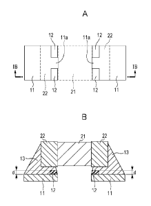
22 of the
2012 size or the 3216 size is equal to or greater than 0.5 mm is used, as the
solder
thickness under the electrode 22, it is possible to allow the thickness
between the
16
CA 02947519 2016-10-31
WO 2015/177988 PCT/JP2015/002423
substrate exposing portion and the lower surface of the electrode 22 to be ap-
proximately 88 micrometers (approximately 18 micrometers corresponding to the
thickness of the land 11 (height of the first stepped portion) + approximately
50 mi-
crometers corresponding to the thickness of the insulating protrusion 12
(height of the
second stepped portion) + approximately 20 micrometers corresponding to the
solder
thickness between the electrode 22 and the insulating protrusion 12), or
approximately
105 micrometers (approximately 35 micrometers corresponding to the thickness
of the
land 11 (height of the first stepped portion) + approximately 50 micrometers
corre-
sponding to the thickness of the insulating protrusion 12 (height of the
second stepped
portion) + approximately 20 micrometers corresponding to the solder thickness
between the electrode 22 and the insulating protrusion 12). That is, in the
third em-
bodiment, when the electronic component 21 in which the width of the short
side of the
electrode 22 is equal to or greater than 0.5 mm is used, it is possible to
allow the
maximum thickness of the solder 13 present within the overlapped region with
the
electrode 22 in the normal direction of the surface of the land 11 to be equal
to or
greater than, for example, 88 micrometers.
[0064] As shown in Figs. 12A and 12B, the planar shape of the land 11 may
be a shape in
which concave portions are formed on two sides facing each other, and may be a
shape
in which two corners of a rectangle are cut off and the width becomes narrower
toward
the other facing land 11.
[0065] In the example shown in Figs. 12A and 12B, the surface of the
substrate 10 is
exposed in the concave portions of the land 11. At least a part of the
substrate
exposing portions and a part of the land 11 sandwiched by the substrate
exposing
portions are included in the overlapped region with the electrode 22 of the
electronic
component 21 in the normal direction of the land surface. Thus, stepped
portions
occurring due to the difference in height between the surface of the land 11
sandwiched by the substrate exposing portions and the substrate exposing
portions po-
sitioned lower than the surface of the land 11 are formed within the
overlapped region
with the electrode 22 of the electronic component 21 in the normal direction
of the
land surface. The solder 13 is interposed between the substrate exposing
portions and
the land 11 and between the substrate exposing portions and the electrode 22,
and the
substrate exposing portions and the land 11, and the substrate exposing
portions and
the electrode 22 are bonded through the solder 13. The solder 13 having a
thickness
greater than the solder thickness between the surface of the land 11 and the
lower
surface of the electrode 22 is interposed between the substrate exposing
portions and
the lower surface of the electrode 22, and the solder thickness between the
substrate
exposing portions and the lower surface of the electrode 22 which is greater
than the
solder thickness between the surface of the land 11 and the lower surface of
the
17
CA 02947519 2016-10-31
WO 2015/177988 PCT/JP2015/002423
electrode 22 is obtained. The solder 13 is bonded to the side surface of the
land 11 on
which the stepped portions are formed, and the bonding area of the solder 13
is
increased. Thus, it is possible to further improve the bonding strength of the
solder
bonding of the electronic component 21. The solder 13 is interposed between
the in-
sulating protrusions 12 and the electrode 22, and the insulating protrusions
12 and the
electrode 22 are bonded through the solder 13. Due to the pair of insulating
pro-
trusions 12, a pair of stepped portions occurring due to the difference in
height
between the insulating protrusions 12 and the surface of the land 11 are
formed while
sandwiching at least a part of a portion where the width of the land 11
becomes
narrow. Thus, the thickness of the solder 13 between the lower surface of the
electrode
22 and the land 11 after the solder melting is obtained, and it is possible to
allow a
large amount of solder 13 to stay between the lower surface of the electrode
22 and the
land 11.
Examples
100661 Hereinafter, the present technology will be described in detail in
conjunction with the
examples. The present technology is not limited to the following
configurations.
Example 1
[0067] A circuit board for a test on which an electronic component (3216
size) has been
mounted with the configuration shown in Figs. 4A to 4C is manufactured. After
solder
bonding, the maximum thickness of the insulating protrusion (silk layer +
resist layer)
with the land surface as a reference was measured, and the measured maximum
thickness thereof was 80 micrometers. The thickness of the resist layer with
the land
surface as a reference was 50 micrometers, and the thickness of the silk layer
was 30
micrometers.
Comparative Example 1
[0068] A circuit board for a test on which an electronic component (3216
size) has been
mounted with a configuration in which the insulating protrusion (silk layer +
resist
layer which constitute the insulating protrusion) is removed from the
configuration
shown in Figs. 4A to 4C was manufactured.
Temperature Cycle Test
[0069] A temperature cycle test in which 125 degrees Celsius for 30 minutes
to 23 degrees
Celsius for 5 minutes to -40 degrees Celsius for 30 minutes to 23 degrees
Celsius for 5
minutes were set as one cycle was performed on the manufactured circuit board.
The
cross section of the solder bonding portion at 750 cycles, 1000 cycles, and
1250 cycles
was observed, and it was checked if cracks and fractures had occurred. A case
where
the cracks and the fractures were not found on the cross section of the solder
bonding
portion was evaluated as OK, and a case where the cracks or the fractures were
found
Is
CA 02947519 2016-10-31
WO 2015/177988 PCT/JP2015/002423
was evaluated as NG.
[0070] The evaluated result is represented in Table 1. In Comparative
Example 1, since the
evaluation at 750 cycles was NG, it is presumed, although not evaluated, that
the
evaluations at 1000 cycles and 1250 cycles are NG. Thus, in Comparative
Example 1,
the evaluations at 1000 cycles and 1250 cycles were not performed.
[0071] [Table 11
750 cycles 1000 cycles 1250 cycles
Example 1 OK OK OK
Comparative Example 1 NG
[0072] As represented in Table 1, in Example 1, it was seen that it was
possible to improve
long-term reliability of the solder bonding as compared to Comparative Example
1.
<4. Another Embodiment>
[0073] The present technology is not limited to the above-described
embodiment of the
present technology, and various modifications and applications are possible
within the
scope that does not depart from the gist of the present technology.
[0074] For example, numerals, structures, shapes, materials, raw materials,
and manu-
facturing processes described in the aforementioned embodiments and examples
are
only examples, and different numerals, structures, shapes, materials, raw
materials and
manufacturing processes may be used when necessary.
[0075] The configurations, methods, steps, shapes, materials and numerals
in the afore-
mentioned embodiments and examples can be combined with each other unless they
depart from the gist of the present technology.
[0076] For example, the layer constituting the insulating protrusions 12
may be a layer other
than the silk layer and the resist layer.
[0077] The present technology may have the following configuration.
<1>
An electronic apparatus comprising:
a substrate;
a conductive land formed on a surface of the substrate;
an electronic component including an electrode;
at least one insulating protrusion formed on the land in an overlapping region
between the land and the electrode in plan view; and
a solder that bonds the electronic component to the land, the solder being
formed
between the electrode and the land in the overlapping region in a normal
direction to
the surface of the substrate.
<2>
The electronic apparatus according to <1>, further comprising a plurality of
the pro-
19
CA 02947519 2016-10-31
WO 2015/177988 PCT/JP2015/002423
trusions that are positioned in the overlapping region near corners of the
electrode in
plan view.
<3>
The electronic apparatus according to any one of <1> to <2>, wherein the
solder is in-
terposed between the protrusion and the electrode in the normal direction.
<4>
The electronic apparatus according to any one of <1> to <3>, wherein the land
includes an extension portion that protrudes from a side of the land in plan
view.
<5>
The electronic apparatus according to <4>, wherein a shape of the extension
portion is
selected from the group consisting of a rectangular shape, a triangular shape,
a curved
shape and a semicircular shape.
<6>
The electronic apparatus according to <5>, wherein at least a portion of the
extension
portion is present in the overlapping region.
<7>
The electronic apparatus according to any one of <1> to <6>, wherein a
thickness of
the solder interposed between the land and the electrode is at least 70 !im in
the normal
direction.
<8>
The electronic apparatus according to any one of <1> to <7>, wherein a
thickness of
the protrusion is at least 40 [tm in the normal direction.
<9>
The electronic apparatus according to any one of <1> to <8>,
wherein when a width of a short side of the electrode is less than 0.5 mm, a
maximum
thickness of the solder is at least 38 [im, and
wherein when a width of a short side of the electrode is greater than 0.5 mm,
a
maximum thickness of the solder is at least 70 [im.
<10>
The electronic apparatus according to any one of <1> to <9>, wherein the
insulating
protrusion includes a resist layer formed on the substrate and on the land,
and includes
an insulating layer formed on the resist layer in the overlapping region.
<11>
The electronic apparatus according to any one of <1> to <10>, wherein a
distance
between a first side edge of the insulating layer and a corresponding first
side edge of
the land in a first direction that is perpendicular to the normal direction
ranges from 0.1
mm to 0.3 mm, and wherein a distance between a second side edge of the
insulating
layer and a corresponding second side edge of the land in a second direction
that is per-
20
CA 02947519 2016-10-31
WO 2015/177988 PCT/JP2015/002423
pendicular to both the normal direction and the first direction ranges from
0.1 mm to
0.3 mm.
<12>
The circuit board according to <10>, wherein a width of the portion of the
resist layer
that is formed on the land is at least 0.3 mm.
<13>
An electronic apparatus according to any one of <1> to <12>, wherein the
electronic
apparatus is a circuit board.
<14>
A battery comprising the electronic apparatus according to any one of <1> to
<12>.
<15>
A power storage device comprising the electronic apparatus according to any
one of
<1> to <12>.
<16>
An electronic device comprising the electronic apparatus according to any one
of <1>
to <12>.
<17>
An electronic apparatus comprising:
a substrate;
a conductive land formed on a surface of the substrate, the land including a
cut out
portion that exposes a portion of the underlying substrate;
an electronic component including an electrode; and
a solder that bonds the electronic component to the land, the solder being
formed
between the electrode and the substrate in the cut out portion of the land in
a normal
direction to the surface of the substrate,
wherein at least part of the cutout portion is in an overlapping region
between the land
and the electrode in plan view.
<18>
The electronic apparatus according to <17>, wherein the solder is also
interposed
between the land and the electrode in the normal direction in the overlapping
region.
<19>
The electronic apparatus according to any one of <17> to <18>, wherein the cut
out
portion includes at least one of an interior portion of the land in plan view,
and a
recessed portion formed into a side of the land.
<20>
The electronic apparatus according to <19>, wherein the cut out portion
includes a
plurality of recessed portions formed into opposed sides of the land.
<21>
21
CA 02947519 2016-10-31
WO 2015/177988 PCT/JP2015/002423
An electronic apparatus comprising:
a substrate;
a conductive land formed on a surface of the substrate;
an electrode or a terminal electrically connecting an electronic component;
at least one insulating protrusion formed on the land in an overlapping region
between
the land and the electrode in plan view; and
a solder that bonds the electrode or the terminal to the land, the solder
being formed
therebetween.
<22>
An electronic apparatus comprising:
a substrate;
a conductive land formed on a surface of the substrate, the land including a
cut out
portion or a dent;
an electrode or a terminal electrically connecting an electronic component;
and
a solder that bonds the electronic component to the land, the solder being
formed
therebetween in the cut out portion or the dent of the land in a normal
direction to the
surface of the substrate.
<23>
There is provided a circuit board including: a substrate; an electronic
component that is
mounted on the substrate, and includes a pair of electrodes which are formed
at both
ends; and a pair of lands that are formed on the substrate, face each other,
and are re-
spectively bonded to the pair of electrodes through solder. At least any one
stepped
portion of a first stepped portion between the land and a substrate exposing
portion at
which the surface of the substrate positioned lower than the land is exposed,
and a
second stepped portion between the land and an insulating protrusion which is
po-
sitioned higher than the land is formed within an overlapped region with the
electrode
in a normal direction of a land surface and protrudes in the normal direction
of the land
surface, and a maximum thickness of the solder within the overlapped region
with the
electrode in the normal direction of the land surface is greater than the
height of at least
any one stepped portion formed within the overlapped region with the electrode
in the
normal direction of the land surface.
<24>
In the circuit board according to <23>, in the electronic component, a width
of a short
side of the electrode is less than 0.5 mm, only the first stepped portion may
be formed
within the overlapped region with the electrode in the normal direction of the
land
surface, and a maximum thickness of the solder present within the overlapped
region
with the electrode in the normal direction of the land surface may be equal to
or greater
than 38 micrometers.
22
CA 02947519 2016-10-31
WO 2015/177988 PCT/JP2015/002423
<25>
In the circuit board according to <23>, in the electronic component, a width
of a short
side of the electrode is equal to or greater than 0.6 mm, only the second
stepped
portion may be formed within the overlapped region with the electrode in the
normal
direction of the land surface, and a maximum thickness of the solder present
within the
overlapped region with the electrode in the normal direction of the land
surface may be
equal to or greater than 70 micrometers.
<26>
In the circuit board according to <23>, in the electronic component, a width
of a short
side of the electrode is equal to or greater than 0.5 mm, both of the first
stepped portion
and the second stepped portion may be formed within the overlapped region with
the
electrode in the normal direction of the land surface, and a maximum thickness
of the
solder present within the overlapped region with the electrode in the normal
direction
of the land surface may be equal to or greater than 88 micrometers.
<27>
There is provided a circuit board including: an electronic component that
includes a
pair of electrodes which are formed at both ends; a pair of lands that face
each other,
and are respectively bonded to the pair of electrodes through solder; and two
groups of
a pair of insulating protrusions that are bonded to the pair of electrodes
through solder,
and protrude in a normal direction of a land surface. One of the pair of lands
protrudes
toward the other land from each of two sides facing each other, and has a
front end
whose part is present within an overlapped region with the electrode in the
normal
direction of the land surface. The pair of insulating protrusions are
separated with at
least a part of the front end of the land interposed therebetween, and are
present within
the overlapped region with the electrode in the normal direction of the land
surface.
<28>
In the circuit board according to <27>, a thickness of the insulating
protrusion from the
land surface may be equal to or greater than 40 micrometers.
<29>
In the circuit board according to <27> or <28>, the insulating protrusion may
include a
single insulating layer or two or more insulating layers.
<30>
In the circuit board according to <29>, the insulating layer may be at least
one of a
resist layer and a silk layer.
<31>
In the circuit board according to <30>, the insulating layer may be the resist
layer and
the silk layer formed on the resist layer, and the silk layer may be disposed
in a vertical
direction such that a longitudinal direction of a planar shape of the silk
layer is sub-
23
CA 02947519 2016-10-31
WO 2015/177988 PCT/JP2015/002423
stantially perpendicular to a protruding direction of the front end.
<32>
In the circuit board according to <30> or <31>, a gap between the silk layer
and the
land may be from 0.1 mm to 0.3 mm.
<33>
In the circuit board according to any one of <27> to <32>, the thickness of
the solder
interposed between the land and a lower surface of the electrode may be equal
to or
greater than 70 micrometers.
<34>
In the circuit board according to any one of <27> to <33>, the shape of the
front end of
the land may be a polygonal shape or a shape including a curved line.
<35>
There is provided a circuit board including: a substrate;
an electronic component that is mounted on the substrate, and includes a pair
of
electrodes which are formed at both ends; and a pair of lands that are formed
on the
substrate, face each other, and are respectively bonded to the pair of
electrodes through
solder. A part of the land and at least a part of a substrate exposing portion
at which
the surface of the substrate is exposed are present within an overlapped
region with the
electrode in a normal direction of a land surface.
<36>
The circuit board according to <25> may further include two groups of a pair
of in-
sulating protrusions that are bonded to the pair of electrodes through solder,
and are
formed to protrude in the normal direction of the land surface. The land may
have a
shape in which the width becomes narrower toward the other facing land, and
the pair
of insulating protrusions may be separated so as to sandwich at least a part
of a portion
where the width of the land becomes narrow, and may be present within the
overlapped region with the electrode in the normal direction of the land
surface.
<37>
There is provided a power storage device including the circuit board according
to any
one of <23> to <36>.
<38>
There is provided a battery pack including the circuit board according to any
one of
<23> to <36>.
<39>
There is provided an electronic device including the circuit board according
to any one
of <23> to <36>.
<5. Application Example>
1100781 The circuit boards according to the first to third embodiments and
another em-
24
CA 02947519 2016-10-31
WO 2015/177988 PCT/JP2015/002423
bodiment are built in, for example, an electronic device, a power storage
device, a
battery pack, and the like.
Power Storage Device
[0079] Examples of a power storage device including the circuit board
include a power
storage device having the configuration shown in Fig. 13. Although not shown,
a
battery unit and a circuit board on which a control circuit block and the like
are
mounted are accommodated within an outer case 90 of the power storage device.
The
circuit board according to the first embodiment or another embodiment of the
present
technology is applied to this circuit board. Although not shown, the battery
unit is a
unit in which a member such as a tab that electrically connects a battery
block group
and a plurality of battery cells is accommodated in a battery case. The
battery block
group includes, for example, a plurality of battery blocks connected to each
other in
series, and one battery block includes a plurality of battery cells connected
in parallel
to each other. The battery cell is, for example, a secondary battery such as a
cylindrical lithium-ion secondary battery. The battery cell is not limited to
the lithium-
ion secondary battery. The battery cell may be a laminated type.
Battery Pack
[0080] Examples of a battery pack including the circuit board include a
battery pack having
the configuration shown in Fig. 14.
[0081] This battery pack is a simple battery pack (also referred to as a
soft pack). The
simple battery pack is built in an electronic device, and is configured in
such a manner
that a battery cell or a protection circuit is fixed by an insulation tape, a
part of the
battery cell is exposed, and an output such as a connector connected to a main
body of
the electronic device is provided.
[0082] An example of the configuration of the simple battery pack will be
described. Fig.
14 is an exploded perspective view showing the configuration example of the
simple
battery pack. Fig. 15A is a schematic perspective view showing the external ap-
pearance of the simple battery pack. and Fig. 15B is a schematic perspective
view
showing the external appearance of the simple battery pack.
[0083] As shown in Figs. 14, 15A, and 15B, the simple battery pack includes
a battery cell
101, leads 102a and 102b extending out of the battery cell 101, insulating
tapes 103a to
103c, an insulating plate 104, a circuit board 105 on which a protection
circuit module
(PCM) is formed, and a connector 106. The circuit board according to the first
em-
bodiment or another embodiment is applied to the circuit board 105.
[0084] The insulating plate 104 and the circuit board 105 are arranged on a
terrace 101a of
the front end of the battery cell 101, and the lead 102a and the lead 102b
extending out
of the battery cell 101 are connected to the circuit board 105.
25
CA 02947519 2016-10-31
WO 2015/177988 PCT/JP2015/002423
[0085] The connector 106 for output is connected to the circuit board 105.
The members
such as the battery cell 101, the insulating plate 104 and the circuit board
105 are fixed
to predetermined portions of the insulating tapes 103a to 103c.
Electronic Device
[0086] Examples of the electronic device including the circuit board
include a notebook
personal computer, a personal digital assistant (PDA), a cellular phone, a
smart phone,
a handset for a cordless phone, a projector, a video camera, a digital still
camera, an
electronic book, an electronic dictionary, a music player, a radio set, a
headphone, a
game machine, a navigation system, a memory card, a pacemaker, a hearing aid,
an
electric tool, an electric shaver, a refrigerator, an air-conditioner, a
television, a stereo,
a water heater, a microwave oven, a dishwashing machine, a laundry machine, a
drying
machine, lighting equipment, a toy, medical equipment, a robot, a server, a
load con-
ditioner, and a traffic light.
[0087] It should be understood by those skilled in the art that various
modifications, com-
binations, sub-combinations and alterations may occur depending on design re-
quirements and other factors insofar as they are within the scope of the
appended
claims or the equivalents thereof.
Reference Signs List
[0088] 1 Circuit board
Substrate
11 Land
11 a Front end
12 Insulating protrusion
13 Solder
14 Resist layer
Silk layer
21 Electronic component
22 Electrode
90 Outer case
101 Battery cell
101a Terrace section
102a, 102b Lead
103a, 103b, 103c Insulating tape
104 Insulating plate
105 Circuit board
106 Connector