Note: Descriptions are shown in the official language in which they were submitted.
CA 02948560 2016-11-16
SEMI-FLEXIBLE SOLAR MODULE USING CRYSTALINE SOLAR CELLS
AND METHOD FOR FABRICATION THEREOF
FIELD
[0001]This present disclosure relates to solar modules and in particular to a
semi-flexible solar
module using crystalline solar cells and method for fabrication thereof.
BACKGROUND
[0002]Solar cells or photovoltaic cells are electrical devices that convert
the energy of light
directly into electricity. Conventionally, a plurality of solar cells are
includes in a solar module,
sometimes known as solar panels. Typically, solar modules include a metal
frame, crystalline
solar cells and a glass cover plate. Since crystalline solar cells can be
fragile, the metal frame
and the glass cover plate are intended to protect the crystalline solar cells
and generally keep the
solar module in predetermined shape.
[0003]Recently, flexible solar modules have been developed using thin-film
solar cells, which
are less fragile than crystalline solar cells and can be rolled up. Thin-film
solar modules tend to
be smaller and for portable use. One drawback of thin-film solar cells is that
they are less efficient
at converting light to electricity than crystalline solar cells.
(0004] As such, there is a need for a semi-flexible solar module that
incorporates crystalline solar
cells.
SUMMARY
[0005]In a first aspect the present disclosure provides a solar module
including: a front layer
having an ultra-violet reflecting material; one or more impact cushion layers;
a solar cell layer
comprising crystalline silicon solar cells; a support layer comprising a semi-
flexible material
configured to support the solar cell layer; and a back layer, wherein none of
the layers is formed
of glass or a material with similar properties as those of glass, including
density, flexibility,
transparency, brittleness and the like.
[0006] In a particular case, the support layer may be transparent and
positioned between the
front layer and the solar cell layer.
[0007]In another particular case, the one or more impact cushion layers also
functions as an
adhesive layer.
1
CA 02948560 2016-11-16
[0008] In still another particular case, the solar module may have a second
impact cushion layer
between the solar cell layer and the support layer.
[0009] In yet another particular case, the solar module may have more adhesive
layers between
the noted layers.
[0010] In still yet another particular case, the solar module may include a
bypass diode provided
to a bus bar on the solar cell layer.
[0011] In a particular case, the bypass diode may have a plurality of bypass
diodes provided to
different bus bars on the solar cell layer.
[0012] In another particular case, the thickness of the module is between 3
and 5mm
[0013] In yet another particular case, the solar module may have low profile
button connectors.
[0014] In still yet another particular case, the front layer includes a
surface pattern. In a particular
case, the surface pattern has a pattern depth between 0.05mm to 0.5mm.
[0015] In another aspect there is provided a solar flexible-solar module
having: a front layer
formed of ETFE; a plurality of impact cushion layers formed of EVA; a solar
cell layer formed of
crystalline silicon solar cells; a support layer formed of PET; and a back
layer formed of TPT.
[0016] In a particular case, the support layer is transparent and positioned
between the front
layer and the solar cell layer.
[0017] In another particular case, the plurality of cushion layers also
functions as adhesive layers.
[0018] In still another particular case, the solar module may include a second
impact cushion
layer between the solar cell layer and the support layer.
[0019] In yet another particular case, the solar module may include one or
more adhesive layers
between the noted layers.
[0020] In still yet another particular case, the solar module includes a
bypass diode provided to
a bus bar on the solar cell layer.
[0021] In a particular case, the bypass diode includes a plurality of bypass
diodes provided to
different bus bars on the solar cell layer.
[0022] In another particular case, the solar module may have a thickness of
the module is
between 3mm and 5mm.
[0023] In still another particular case, the solar module further may include
low profile button
connectors.
[0024] In yet another particular case, the front layer of the solar module has
a surface pattern.
2
CA 02948560 2016-11-16
[0025] In a particular case, the surface pattern has a pattern depth between
0.05mm to 0.5mm.
[0026] In yet another aspect, there is provided a method for applying a
pattern sheet to a solar
module including: placing solar module layers in order to create the solar
module; placing a
pattern sheet on a top layer of the solar module; laminating the solar module;
and cooling the
solar module.
[0027] In a particular case, the lamination of the solar module includes:
providing a vacuum to
the solar module; and providing a retaining period to the solar module.
[0028] In another particular case, the retainer period is 10 ¨ 18 minutes in
duration at a press
pressure of 60 to 85 kPa and at a temperature of 145 C to 155 C.
[0029] In still another particular case, the cooling of the solar module
includes placing a heavy
object on top of the pattern sheet to maintain the pattern shape.
(0030] Other aspects and features of the present disclosure will become
apparent to those
ordinarily skilled in the art upon review of the following description of
specific embodiments in
conjunction with the accompanying figures.
BRIEF DESCRIPTION OF THE DRAWINGS
[0031]Embodiments of the invention will now be described, by way of example
only, with
reference to the attached drawings, in which:
[0032] Fig. 1 illustrates an embodiment of a flexible solar module;
[0033] Fig. 2 illustrates another embodiment of a semi-flexible solar module;
[0034] Fig. 3 illustrates yet another embodiment of a semi-flexible solar
module;
[0035] Fig. 4 illustrates still yet another embodiment of a semi-flexible
solar module;
[0036] Fig. 5 illustrates an example of bus bars and bypass diodes in the semi-
flexible solar
module of Fig. 1 with junction box;
[0037] Figs. 6A and 6B illustrate an embodiment of connectors for the semi-
flexible solar module
of Fig. 1 in series and in parallel;
[0038] Fig. 7 illustrates an embodiment of a junction box for use with the
connectors of Fig. 5;
[0039] Fig. 8 illustrates a close up of a bypass diode laminated in a solar
module;
[0040] Fig. 9 illustrates an example of a surface pattern applied to a front
layer of the semi-flexible
solar module of Fig. 1 from a top view and side view; and
[0041] Fig. 10 is a flow chart of a method for applying a pattern to a surface
for a solar module.
3
CA 02948560 2016-11-16
DETAILED DESCRIPTION
(0042] Generally, the disclosure provides for a semi-flexible solar module
using crystalline solar
cells. The disclosure also relates to an electrical connection device for a
semi-flexible solar
module and a surface pattern for a semi-flexible solar module. Allowing for
some flexibility, the
solar module is intended to have a greater range of uses than a rigid solar
module. The semi-
flexible solar module is also intended to weigh less than a conventional solar
module.
[0043]The semi-flexible module is intended to be easily cold bent to conform
to the curvature at
the location of installation. The solar module is intended to be light weight,
so transportation
becomes cheaper and facilitates its assembly. Further, the surface finish may
allow a self-
cleaning behavior because it is non-stick material and may minimize surface
tension due to its
texture. The solar module may be affixed with adhesive or screws.
[0044] Figure 1 illustrates an embodiment of a semi-flexible solar module 100.
In this
embodiment, the solar module 100 includes a front layer 105, an impact cushion
layer 110, a
solar cell layer 115, a support layer 120, and a back layer 125.
[0045] Figure 2 illustrates another embodiment of a semi-flexible solar module
200. The
embodiment of Fig. 2 is similar to that of Fig. 1, except that an additional
impact cushion layer
110 has been provided between the solar cell layer 115 and the support layer
120.
(0046] Figure 3 illustrates a further embodiment of a semi-flexible solar
module 300. In this
embodiment, the support layer 120 and solar cell layer 115 of Fig. 2 have been
switched in
position such that the support layer 120 is now above the solar cell layer 115
and between the
two impact cushion layers 110. In some cases, placing the support layer 120
above the solar cell
layer 115 is intended to enhance the cushion layers to prevent outside impact.
In other cases, the
solar layer 115 may be placed above as this configuration may improve light
transmission being
above the support layer.
(0047] The front layer 105 is transparent and is intended to provide some
protection to the solar
module. In particular, the front layer 105 may provide ultra-violet (UV)
protection to reduce or
prevent sub-layer degradation from sun exposure. The front layer 105 may be
made from at least
one material selected from a group of ethylene tetrafluorethylene (ETFE),
ethylene
chlorotrifluoroethylene, polyvinyl fluoride film, ethylene propylene
copolymer. The front layer may
have thickness between 0.025 to 0.1mm. Depending on the material chosen, the
front layer is
intended to provide:
4
CA 02948560 2016-11-16
a. superior adhesion to sub-layer (possibly via surface treatment);
b. excellent dielectric strength to help make the front layer 105 an effective
insulator;
c. good mechanical strength (tear strength) and dimensional stability;
d. protection against moisture; and
e. low surface energy so the front layer 105 will stay cleaner and can be
cleaned
easily.
[0048] The impact cushion layer 110 is intended to absorb impact energy, such
as from hail,
snow, wind-borne solid debris, and the like, to prevent damage to the solar
cells within the solar
cell layer 115. The impact cushion layer 110 may generally be disposed
adjacent to the solar cell
layer 115. In some cases, the impact cushion layer 110 may be provided on both
sides of the
solar cell layer 115 to provide for greater protection. In some cases, the
impact cushion layer may
also serve as an adhesive between the front layer 105 and the solar cell layer
115 and/or between
the solar cell layer 105 and the support layer 120 and/or other layers in the
stack. The impact
cushion layer 110 may be at least one material selected from a group of
ethylene vinyl acetate
(EVA), silicone sealant, epoxy, polyolefin, butyl rubber based adhesive, or
vinyl phenolic.
[0049] The solar cell layer 115 is formed from monocrystalline or
polycrystalline silicon cells.
These silicon cells may be a conventional size, such as 156mmx156mm, or may be
other sizes
of cells that are mounted in the solar cell layer 115. In a solar panel, cells
may be connected in
series with, for example, a metal ribbon or the like. Each solar cell may be
manually or
automatically soldered together or may use electrical conductive adhesive to
bond the solar cell
to the metal ribbon.
[0050]The support layer 120 is configured to have sufficient load bearing
properties that the
supporting layer 120 can support the solar cell layer 115 such that the solar
cell layer 115 will not
break. As such, the supporting layer 120 may be rigid or semi-flexible and may
be fabricated from
at least one material selected from a group of polyethylene terephthalate
(PET), polyurethane,
polyetherimide, polyvinylidene fluorid, ethylene vinyl acetate, polyester,
fiber glass sheet, coated
dielectric plastic aluminum or stainless steel sheet, carbon fiber reinforced
thermoplastic, and
glass fiber reinforced thermoplastic. In some embodiments, if the support
layer is placed above
the solar cells, the support layer, for example, the PET, is intended to be
transparent and have a
thickness of no more than approximately 0.5mm. In some cases, the thickness
may be
approximately 0.25mm. If the support layer is placed below the solar cell
layer, the material may
have a thickness between 0.2mm and 2mm.
CA 02948560 2016-11-16
[0051] In some cases, the support layer 120 may be transparent and may be
placed above the
solar cell layer 115. It is intended that placing the support layer 120 above
the solar cell layer 115,
will provide further protection to the solar cell layer 115 from impacts and
the like. As illustrated in
Fig. 2 and 3, in some cases, the support layer 120 may be provided above the
solar cell layer 115
and impact cushion layers 110 may be above and below the support layer 120 as
well as below
the solar cell layer 115 in order to provide for softer layers for impact
protection but also include
impact protection from the support layer 120.
[0052] The back layer 125 is intended to provide different physical or
chemical properties offering
protection from a wide range of environmental elements. The properties may
include for example:
mechanical strength, UV resistance, dielectric strength, thermal stability,
hydrolytic stability, and
moisture resistance. The back layer 125 can be either rigid or semi-flexible
and may be selected
from tedlar polyester tedlar (TPT), kynar film/PTE/EVA (KPE), Themoplastic
elastomer (TPE),
coated aluminum sheet, coated stainless sheet, fiberglass, carbon fiber
reinforced thermoplastic,
glass fiber reinforced thermoplastic. The back layer 120 thickness may be
between 0.5mm to
3mm. It will be understood that the crystalline solar cell is fragile while
the thin film solar cells may
be rolled up. It is intended that the semi-flexible solar panel use
crystalline solar cells and may be
bent approximately 30 degrees within lm length with 800mm radius curve.
[0053] In some cases, the back layer 120 may include a plurality of sub-
layers, for example, a
PET sub-layer as a middle sub-layer or upper sub-layer and may include a
second material for at
least one other layer of the back layer 120. The second layer could be
fabricated from, for
example, polyvinyl fluoride (PVF), or polyvinylidene fluoride (PVDF), a
thermoplastic
fluoropolymer material which features high water-resistance and inherent
strength, has low
permeability of moisture, vapor, oil and may be used in a wide temperature
range of for example,
between -70 C to + 110 C.
[0054] In each of the above embodiments, one or more adhesive layers 130 may
be provided
between the various layers in order to maintain bonding where the layer
material itself cannot be
used in creating a bond between layers. In some cases, an adhesive layer 130
may also function
as an impact cushion layer 110.
[0055] In the above embodiments, the semi-flexible solar panel is formed
without a glass layer in
order to provide flexibility, reduce weight, make the panel less suceptible to
breakage and the
like. The use of crystaline solar cells is intended to provide improved energy
conversion efficiency
when compared with thin-film solar cells of the type that are typically used
in flexible solar cells.
6
CA 02948560 2016-11-16
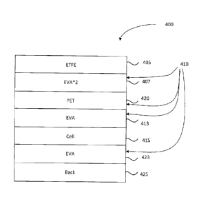
[0056] Figure 4 illustrates another embodiment of a solar module 400. Fig. 4
illustrates specific
materials for each of the above noted layers in the solar module 400
[0057] In this particular embodiment, the front layer 405 is ethylene
tetrafluoroethylene (ETFE),
a fluorine-based plastic. The nature of this plastic allows for UV protection
and other properties,
for example, high transmittance (greater than or equal to 92%), high
dielectric strength, which is
intended to help make the layer an effective insulator, good mechanical
strength and moisture
permeability. Those properties may be needed for the front layer. The front
layer 405 may be
followed by a first adhesive layer 407 of ethylene-vinyl-acetate (EVA) for
bonding to a support
layer 420. In some cases, the first adhesive layer 407 may include two or more
sub-layers of
ethylene-vinyl-acetate (EVA). In this embodiment, the first adhesive layer 407
may also serve as
an impact cushion layer 410.
[0058] The support layer 420 is polyethylene terephthalate (PET). In this
case, the support layer
420 may also act as an impact cushion layer 410. A second adhesive layer 413
(also formed of
EVA) then adheres the support layer 420 to the solar cell layer 415. A third
adhesive layer 423
(also formed of EVA) adheres the solar cell layer 415 to the back layer 425.
The second and third
adhesive layers 413, 423 and may also serve as further impact cushion layers
410 for the solar
cell layer 415.
[0059]The back layer 120 may be formed of Toyal FPL which may have an
approximate
thickness of 0.375mm. FPL is intended to have high tensile strength,
dimensional stability, and
low permeability of water vapor. In this example, an ETFE layer may be about
0.05mm, an EVA
layer may be between 0.45mm and 0.5mm, a PET layer may be about 0.25mm, the
solar cell
layer may be 0.20mm and a back layer, which may be FPL, TPT or KPE may be
about 0.375mm.
[0060] Generally, the embodiments of the semi-flexible solar module described
herein are made
without glass in order to allow the solar module to have some degree of
flexibility. Further, the
solar module generally does not require an aluminum frame which may be
approximately 40 to
50% of a conventional module's weight. For example, a conventional solar
module's weight
loading may be approximately 11kg/M2, whereas the semi-flexible solar module
provided herein
is intended to have a weight loading of approximately 4 kg/M2 to 5kg/M2. In
some specific cases,
the weight loading may be approximately 4.6kg/M2. The solar module is intended
to include a
combination of high efficiency, low cost crystalline silicon cells with a
lightweight, rigid or semi-
flexible substrate structure. In some cases, it is intended that the semi-
flexible structure would
allow for approximately 30 degree solar module bending. The total module
thickness is intended
7
CA 02948560 2016-11-16
to be between 2mm to 8mm. In some particular cases, the solar module thickness
may be
between 3mm to 5mm.
[0061] Figure 5 illustrates a solar cell layer 115 in further detail. As shown
in Fig. 5, the solar cell
layer 115 will include a plurality of solar cells and bus bars that extend
across the solar cells on
both sides in order to interconnect the solar cells and allow electricity to
flow from and through
the solar cells as it is produced. The bus bars may be provided to the solar
cell layer 115 by any
conventional method, for example, by conventional soldering techniques, either
manually or
automatically. In other cases, the bus bars may be bonded to the solar cell
layer 115 by electrically
conductive adhesive (ECA). In at least some cases of the present embodiments,
the bus bars will
be covered by, for example, the impact cushion layer 110 and the front layer
105 during the
lamination process.
[0062] Figure 6A illustrates low profile button connectors 500 in series
connection according to
an embodiment herein. The button connector 500 includes a socket 510 and a
stud 505 that are
installed on a front or back side of the solar module 100 respectively. As
shown in Fig. 6, the
button connector 500 is embedded in the layers of the solar module. The socket
505 and stud
510 each make contact with the bus bars, and in particular the male connector
520 and female
connector 515 on the bus bar on their respective sides of the solar module.
Solar modules may
then be connected by press fitting the stud 510 into the socket 505 as
illustrated in Fig. 6A or use
additional connection cable to be connected together.
[0063] Figure 6B illustrates low profile button connectors 550 in parallel
connection. Similarly to
Figure 6A, Figure 6B includes a male stud 555 and female socket 560 located on
the solar module
and configured to connect via press fitting to be connected together in a
parallel manner to
corresponding connectors, 565 and 570. It will be understood that the
connectors will be fully filled
in order to ensure that there is no hole. In some cases the filler may be
silicone or similar material.
The bus bars may be covered with string tape to be insulated to prevent
touching from other
conductive material which may cause an electrical short.
[0064] Figure 7 illustrates a junction box 600 provided to a bus bar 605 on
the solar cell layer
105. The bus bars 605 may connect to a junction box terminal 610 by, for
example, soldering. If
the module power is equal to or no more than 100W, the junction box may
contain one bypass
diode. If the module power is above 100W, the junction box may not contain
bypass diode, but
the bypass diodes may instead be integrated into the solar module.
8
CA 02948560 2016-11-16
[0065] Figure 8 illustrates the provision of one or more diodes 700 on a bus
bars 705 in an
alternative embodiment. The one or more diodes 700 are bypass diodes, which
are intended to
protect the solar cells 710 from hot-spot risk, such as, for example, when
there is shade or some
type of damage to one or more of the solar cells 710, wherein the solar cells
710 are connected
to the bus bars 705 via conductive ribbon 715. Typically one bypass diode is
provided per string
of solar cells. In a conventional solar module, the bypass diodes are provided
in the junction box.
However, in at least some embodiments herein, the bypass diodes are provided
directly on the
bus bars and are included in the lamination of the various layers of the solar
module.
[0066]Conventional bypass diodes used in cell based solar panels may serve as
a protection
mechanism that allows the panel to continue producing power even if one or
more of its cell strings
is not working, for example, shaded, damaged, or the like. Typically, all
strings may be connected
in series and each cell attempts to produce current in direct proportion to
the amount of sunlight
it receives. If any of the cells begin to function at a reduced capacity, for
example, the cell is
shaded, soiled, damaged or the like, the entire string current may be limited
to that which the
weakest cell can support. In these conditions, the panel does not operate at
full power.
[0067] A typical cell may have a forward voltage of approximately 0.5V when
optimally loaded. If
the cell is, for example, shaded, the cell may not produce as much current as
other nearby cells,
then the cell may be forced into a reverse mode of operation where it is
subjected to negative
voltage. The underperforming cell may become a heating element, creating a hot
sport on the
solar module which may damage the solar module. In order to prevent these
issues, it is intended
that a series of cells of the solar module be arranged in string and a bypass
diode may be
connected in parallel to each string.
[0068] The connectors are intended to use low profile and compact form factors
to be integrate
into the solar module. In some cases the thickness may be approximately 0.7 mm
which is
intended to make the lamination process easier and smoother than traditional
processes. The
solar module thickness is intended to be between 3mm to 5mm. The diodes may be
soldered with
the bus bar between two strings. With integrated diodes, it may be feasible to
use more diodes
per solar module, allowing the remaining substrings to continue to produce in
partial shaded
conditions.
[0069] In some embodiments, the solar module may be configured to include a
surface pattern
900 on the front layer 405 as shown in Figure 9, which illustrates a pattern
sheet on the surface
of the solar module shown in figure 4. The surface pattern 900 may be created
mechanically or
9
CA 02948560 2016-11-16
through, for example, pressure treating the front layer 405. The surface
pattern 900 is intended
to prevent surface wrinkles during module processing and reduce sun reflective
loss and increase
module output efficiency. In some conventional solar modules, severe surface
wrinkling has been
observed. The embodiments of the solar module herein may include a special
pattern sheet
applied to the surface of the front layer 405, for example during module
processing, which is
intended to provide consistent surface angle contact due to a predetermined
profile. The
predetermined profile can be one of various patterns, including dimple
pattern, triangle pattern,
rectangle pattern, square pattern, and linear cross-hatching pattern. The
pattern depth is
preferably between 0.05mm to 0.5mnn. By providing a cross-hatching pattern
sheet on the front
layer 405 of the solar module, it was noted that there was either a reduction
or an elimination of
the surface wrinkle and the solar module was able to maintain light
penetration efficiency of more
than 90%. The surface pattern sheet can be selected from one of group from
high temperature
pattern plastic, cross-hatching fiber Teflon sheet, textured fiberglass,
coated metal sheet.
[0070] Figure 10 illustrates a method for applying a pattern sheet to a solar
module. At 1005,
materials are placed in order to create a solar module. At 1010, a pattern
sheet is placed onto the
top layer of the solar module. At 1015, the solar panel is sent to a
laminator. The lamination
process may include vacuum, for example for 3 to 8 minutes, followed by
retaining for a period
of, for example, 10 to 18 minutes with press pressure of approximately 60 to
85 kpa and at a
temperature of approximately 145 to 155 C. At 1020, the solar module may be
cooled after it is
removed from the laminator. In some cases a heavy flat plate or similar object
may be placed on
top of the pattern sheet for a period of time to maintain the pattern shape
during the cooling. The
module may sit on an unloading convey to cool down after lamination. In some
cases a heavy flat
plate or similar object may be placed on top of the pattern sheet for a period
of time in order to
maintain pattern shape and to prevent module warping during the cooling
[0071]The local surface treatment is intended to increase surface energy
leading to superior
bonding strength to junction box or other connector touching the surface. The
local surface can
be treated by one of techniques like corona (under 02/N2, N2, N2/CO2, or the
like), flame treatment,
atmospheric plasma activation, and atmospheric or low pressure plasma
deposition.
[0072] In the preceding description, for purposes of explanation, numerous
details are set forth
in order to provide a thorough understanding of the embodiments. However, it
will be apparent to
one skilled in the art that these specific details are not required. In other
instances, well-known
electrical structures and circuits are shown in block diagram form in order
not to obscure the
CA 02948560 2016-11-16
understanding. For example, specific details are not provided as to whether
the embodiments
described herein are implemented as a software routine, hardware circuit,
firmware, or a
combination thereof.
[0073]The above-described embodiments are intended to be examples only.
Alterations,
modifications and variations can be effected to the particular embodiments by
those of skill in the
art without departing from the scope, which is defined solely by the claims
appended hereto.
11