Note: Descriptions are shown in the official language in which they were submitted.
81801113 (88296-3)
COVER ASSEMBLIES, KITS AND METHODS FOR COVERING ELECTRICAL
CABLES AND CONNECTIONS
[001]
Field of the Invention
[002] The present invention relates to electrical cables and connections and,
more
particularly, to protective covers for electrical cables and electrical
connections.
Background
[003] In the electrical utilities industry, maintaining cable integrity may be
critical. A
loss of cable integrity, for example, a short circuit in a high voltage cable,
may result in a
crippling power outage or, even worse, a loss of life. One everyday task that
may pose a great
threat to cable integrity is the formation of electrical connections.
[004] When electrical connections are folined, a bare metal surface may be
exposed
such as a splice connector. If the connection is made between two insulated
cables, it is
assumed the connection is in a harsh environment, such as a water-filled duct
or buried under
rocks. In turn, it is necessary to effectively rebuild the cable's electrical
insulation, metallic
shield, and environmental protection over this connection. If the connection
was energized
without rebuilding the cable layers, the metallic connection may fail
immediately or very soon
after. Thus, there is a need to protect such electrical connections from the
environment.
[005] Many power networks require electrical shielding that is broken into
sections to
prevent lossy circulating currents. A splice connection is a good place to
provide a shield break
because the shielding is already cut during splicing and must be remade during
the splice
installation. The shield break may, however, allow the two adjacent shield
networks to have a
high electric potential difference relative to each other due to magnetic
induction caused by the
current in the main power conductor. The splice must withstand high voltages
on each side of
its shields due to this phenomenon.
1
CA 2948616 2019-06-19
81801113 (88269-3)
Summary
[006] According to a first aspect of the present invention, a cover assembly
is provided
for covering and electrically insulating an electrical connection between
first and second
electrical cables. The cover assembly includes a joint body including a
tubular inner sleeve, an
integral semiconductor layer and a tubular, metal shield layer surrounding the
semiconductor
layer. The tubular inner sleeve is formed of an elastically expandable,
electrically insulating
material and having an outer surface and opposed first and second terminal
ends. The inner
sleeve defines a through passage extending axially from a first end opening at
the first terminal
end of the inner sleeve to a second terminal end opening at the second end of
the inner sleeve.
The integral semiconductor layer is disposed on the outer surface of the inner
sleeve and is
formed of an electrically semiconductive material. The semiconductor layer
extends axially
from a first terminal end of the semiconductor layer to an opposing second
terminal end of the
semiconductor layer. The tubular, metal shield layer is surrounding the
semiconductor layer,
wherein the first terminal end of the semiconductor layer is spaced apart from
the first terminal
end of the inner sleeve by a semiconductor truncation distance (L3) to define
a tubular band of
the outer surface that is not covered by the semiconductor layer, and wherein
the metal shield
layer extends axially from a first terminal end of the metal shield layer to
an opposing second
terminal end of the metal shield layer. The first terminal end of the metal
shield layer is spaced
apart from the first terminal end of the inner sleeve by a shield truncation
distance (L4) to define
a tubular band of the outer surface that is not covered by the metal shield
layer. The metal shield
layer includes a shield extension section configured to be extended axially
beyond the second
terminal end of the inner sleeve. The cover assembly further comprises: a
flowable, first
electrically insulating void filler material for mounting in an annular gap
(G) definable
between the first terminal end of the inner sleeve and a first cable shield of
the first
electrical cable when mounting the cover assembly on the first and second
electrical cables,
to electrically isolate the metal shield layer from the first cable shield and
thereby provide a
shield break (SB) between the first cable shield and a second cable shield of
the second
electrical cable; and a flowable second electrically insulating material for
surrounding the
first electrically insulating void filler material, wherein the first
electrically insulating void
filler material is softer than the second electrically insulating material.
2
Date Recue/Date Received 2020-04-09
81801113 (88269-3)
[006A] In some embodiments, the first terminal end of the metal shield layer
may also
be spaced apart from the first terminal end of the semiconductor layer a
prescribed axial
distance to define a tubular band of the semiconductor layer that is not
covered by the metal
shield layer. The second terminal end of the semiconductor layer extends to
the second terminal
end of the inner sleeve or is axially spaced therefrom a second semiconductor
truncation
distance that is less than the prescribed semiconductor truncation distance.
[007] According to another aspect, a method is provided for forming a
protected
connection assembly. The method includes forming an electrical connection
between first and
second electrical cables, and providing a cover assembly. The cover assembly
includes a joint
body including a tubular inner sleeve, an integral semiconductor layer and a
tubular, metal
shield layer surrounding the semiconductor layer. The inner sleeve is formed
of an elastically
expandable, electrically insulating material and having an outer surface and
opposed first and
second terminal ends. The inner sleeve defines a through passage extending
axially from a first
end opening at the first terminal end of the inner sleeve to a second terminal
end opening at the
second end of the inner sleeve. The integral semiconductor layer is disposed
on the outer
surface of the inner sleeve and is formed of an electrically semiconductive
material. The
semiconductor layer extends axially from a first terminal end of the
semiconductor layer to an
opposing second terminal end of the semiconductor layer and a tubular, metal
shield layer
surrounding the semiconductor layer. The first terminal end of the
semiconductor layer is
spaced apart from the first terminal end of the inner sleeve by a
semiconductor truncation
distance (L3) to define a tubular band of the outer surface that is not
covered by the
semiconductor layer. The method further includes mounting the cover assembly
on the first and
second electrical cables such that the first and second electrical cables and
the electrical
connection extend through the inner sleeve, the first electrical cable extends
out of the inner
sleeve through the first end opening, and the second electrical cable extends
out of the inner
sleeve through the second end opening wherein: the metal shield layer extends
axially from a
first terminal end of the metal shield layer to an opposing second terminal
end of the metal
shield layer; the first terminal end of the metal shield layer is spaced apart
from the first terminal
end of the inner sleeve by a shield truncation distance (L4) to define a
tubular band
3
Date Recue/Date Received 2020-04-09
81801113 (88269-3)
of the outer surface that is not covered by the metal shield layer; the metal
shield layer includes
a shield extension section configured to be extended axially beyond the second
end of the inner
sleeve. The method further comprises extending the shield extension to axially
overlap and
electrically contact a semiconductor layer of the second electrical cable; and
when the protected
connection assembly is formed, the metal shield layer does not contact a
semiconductor layer of
the first electrical cable. When the protected connection assembly is formed,
an annular gap
(G) is defined between the first terminal end of the inner sleeve and a first
cable shield of
the first electrical cable to electrically isolate the metal shield layer from
the first cable
shield and thereby provide a shield break (SB) between the first cable shield
and a second
cable shield of the second electrical cable, the method including mounting a
flowable, first
electrically insulating void filler material in the gap, and mounting a
flowable second
electrically insulating material to surround the first electrically insulating
void filler
material, wherein the first electrically insulating void filler material is
softer than the
second electrically insulating material.
[007a] In some embodiments, the second terminal end of the semiconductor layer
extends to
the second terminal end of the inner sleeve or is axially spaced therefrom a
second
semiconductor truncation distance that is less than the prescribed
semiconductor truncation
distance.
[008] According to another aspect, a protected connection assembly is provided
including first and second electrical cables, an electrical connector forming
an electrical
connection between the first and second electrical cables, and a cover
assembly comprising: a
joint body including a tubular inner sleeve, an integral semiconductor layer
and a tubular, metal
shield layer surrounding the semiconductor layer. The inner sleeve is formed
of an elastically
expandable, electrically insulating material and having an outer surface and
opposed first and
second terminal ends. The inner sleeve defines a through passage extending
axially from a first
end opening at the first terminal end of the inner sleeve to a second terminal
end opening at the
second end of the inner sleeve. The integral semiconductor layer is disposed
on the outer
surface of the inner sleeve and is formed of an electrically semiconductive
material. The
semiconductor layer extends axially from a first terminal end of the
semiconductor layer to an
opposing second terminal end of the semiconductor layer; and a tubular, metal
shield layer
3a
Date Recue/Date Received 2020-04-09
81801113 (88269-3)
surrounding the semiconductor layer. The first terminal end of the
semiconductor layer is
spaced apart from the first terminal end of the inner sleeve by a
semiconductor truncation
distance (L3) to define a tubular band of the outer surface that is not
covered by the
semiconductor layer. The cover assembly is mounted on the first and second
electrical cables
such that the first and second electrical cables and the electrical connection
extend through the
inner sleeve, the first electrical cable extends out of the inner sleeve
through the first end
opening, and the second electrical cable extends out of the inner sleeve
through the second end
opening; and wherein the metal shield layer extends axially from a first
terminal end of the
metal shield layer to an opposing second terminal end of the metal shield
layer; the first terminal
end of the metal shield layer is spaced apart from the first terminal end of
the inner sleeve by a
shield truncation distance (L4) to define a tubular band of the outer surface
that is not covered
by the metal shield layer; and the metal shield layer includes a shield
extension section
extending axially beyond the second terminal end of the inner sleeve. The
cover assembly
further comprises: a flowable, first electrically insulating void filler
material mounted in an
annular gap (G) defined between the first terminal end of the inner sleeve and
a first cable shield
of the first electrical cable, to electrically isolate the metal shield layer
from the first cable shield
and thereby provide a shield break (SB) between the first cable shield and a
second cable shield
of the second electrical cable; and a flowable second electrically insulating
material surrounding
the first electrically insulating void filler material, wherein the first
electrically insulating void
filler material is softer than the second electrically insulating material.
[008A] In some embodiments, the second terminal end of the semiconductor layer
extends to the second terminal end of the inner sleeve or is axially spaced
therefrom a second
semiconductor truncation distance that is less than the prescribed
semiconductor truncation
distance.
[008B] According to another aspect, a cover assembly is provided for covering
and
electrically insulating an electrical connection, the cover assembly
comprising: a joint body
including: a tubular inner sleeve formed of an elastically expandable,
electrically insulating
material and having an outer surface and opposed first and second terminal
ends, the inner
sleeve defining a through passage extending axially from a first end opening
at the first terminal
end of the inner sleeve to a second terminal end opening at the second end of
the inner sleeve;
3b
Date Recue/Date Received 2020-04-09
81801113 (88269-3)
and an integral semiconductor layer on the outer surface of the inner sleeve
and formed of an
electrically semiconductive material, the semiconductor layer extending
axially from a first
terminal end of the semiconductor layer to an opposing second terminal end of
the
semiconductor layer; wherein the first terminal end of the semiconductor layer
is spaced apart
from the first terminal end of the inner sleeve a prescribed semiconductor
truncation distance to
define a tubular band of the outer surface that is not covered by the
semiconductor layer; and
wherein the second terminal end of the semiconductor layer is located
substantially at the
second terminal end of the inner sleeve.
[008C] According to another aspect, a cover assembly is provided for covering
and
electrically insulating an electrical connection between first and second
electrical cables, the
cover assembly comprising: a joint body including: a tubular inner sleeve
formed of an
elastically expandable, electrically insulating material and having an outer
surface and opposed
first and second terminal ends, the inner sleeve defining a through passage
extending axially
from a first end opening at the first terminal end of the inner sleeve to a
second terminal end
opening at the second end of the inner sleeve; wherein the first terminal end
of the
semiconductor layer is spaced apart from the first terminal end of the inner
sleeve a first
semiconductor truncation distance (L3) to define a tubular band of the outer
surface that is not
covered by the semiconductor layer; and a removable holdout device mounted
within the inner
sleeve, wherein the holdout device is operative to temporarily maintain the
inner sleeve in a
radially expanded state; wherein: the metal shield layer extends axially from
a first terminal end
of the metal shield layer to an opposing second terminal end of the metal
shield layer; the first
terminal end of the metal shield layer is spaced apart from the first terminal
end of the inner
sleeve a shield truncation distance (L4) to define a tubular band of the outer
surface that is not
covered by the metal shield layer; and the metal shield layer includes a
shield extension section
configured to be extended axially beyond the second terminal end of the inner
sleeve; the
second terminal end of the semiconductor layer extends to the second terminal
end of the inner
sleeve or is axially spaced therefrom a second semiconductor truncation
distance that is less than
the first semiconductor truncation distance (L3); and when the cover assembly
is mounted on
the electrical connection, an annular gap (G) is defined between the first
terminal end of the
inner sleeve and a first cable shield of the first cable to electrically
isolate the metal shield layer
3c
Date Recue/Date Received 2020-04-09
81801113 (88269-3)
from the first cable shield and thereby provide a shield break (SB) between
the first cable shield
and a second cable shield of the second cable.
[008D] According to another aspect, a method is provided for forming a
protected
connection assembly, the method comprising: forming an electrical connection
between first and
second electrical cables; providing a cover assembly including: a joint body
including: a tubular
inner sleeve fornled of an elastically expandable, electrically insulating
material and having an
outer surface and opposed first and second terminal ends, the inner sleeve
defining a through
passage extending axially from a first end opening at the first terminal end
of the inner sleeve to
a second end opening at the second terminal end of the inner sleeve; an
integral semiconductor
layer on the outer surface of the inner sleeve and formed of an electrically
semiconductive
material, the semiconductor layer extending axially from a first terminal end
of the
semiconductor layer to an opposing second terminal end of the semiconductor
layer; and a
tubular, metal shield layer surrounding the semiconductor layer; wherein the
first terminal end
of the semiconductor layer is spaced apart from the first terminal end of the
inner sleeve a first
semiconductor truncation distance (L3) to define a tubular band of the outer
surface that is not
covered by the semiconductor layer; and a removable holdout device mounted
within the inner
sleeve, wherein the holdout device temporarily maintains the inner sleeve in a
radially expanded
state; and mounting the cover assembly on the first and second cables such
that the first and
second cables and the electrical connection extend through the inner sleeve,
the first cable
extends out of the inner sleeve through the first end opening, and the second
cable extends out
of the inner sleeve through the second end opening; and thereafter removing
the holdout device
from the inner sleeve to permit the inner sleeve to radially retract onto the
first and second
cables and the electrical connection; wherein: the metal shield layer extends
axially from a first
terminal end of the metal shield layer to an opposing second terminal end of
the metal shield
layer; the first terminal end of the metal shield layer is spaced apart from
the first terminal end
of the inner sleeve a shield truncation distance (L4) to define a tubular band
of the outer surface
that is not covered by the metal shield layer; the metal shield layer includes
a shield extension
section configured to be extended axially beyond the second end of the inner
sleeve; the method
includes extending the shield extension to axially overlap and electrically
contact a
semiconductor layer of the second cable; when the protected connection
assembly is formed, the
3d
Date Recue/Date Received 2020-04-09
81801113 (88269-3)
metal shield layer does not contact a semiconductor layer of the first cable;
the second terminal
end of the semiconductor layer extends to the second terminal end of the inner
sleeve or is
axially spaced therefrom by a second semiconductor truncation distance that is
less than the first
semiconductor truncation distance (L3); and when the cover assembly is mounted
on the
electrical connection, an annular gap (G) is defined between the first
terminal end of the inner
sleeve and a first cable shield of the first cable to electrically isolate the
metal shield layer from
the first cable shield and thereby provide a shield break (SB) between the
first cable shield and a
second cable shield of the second cable.
[009] Further features, advantages and details of the present invention will
be
appreciated by those of ordinary skill in the art from a reading of the
figures and the detailed
description of the preferred embodiments that follow, such description being
merely illustrative
of the present invention.
Brief Description of the Drawings
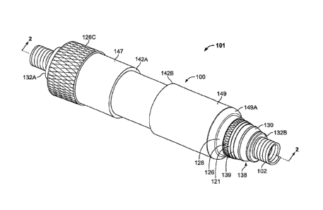
[0010] FIG. 1 is a perspective view of a pre-expanded unit according to
embodiments of
the present invention.
[0011] FIG. 2 is a cross-sectional view of the pre-expanded unit of FIG. 1
taken along
the line 2-2 of FIG. 1.
3e
Date Recue/Date Received 2020-04-09
CA 02948616 2016-11-09
WO 2015/175623
PCT11JS2015/030508
[0012] FIG. 3 is a fragmentary, cross-sectional view of a protected connection
assembly including a cover assembly and cover system according to embodiments
of the
present invention.
[0013] FIG. 4 is a fragmentary, perspective, cross-sectional view of the
protected
connection assembly of FIG. 3.
[0014] FIG. 5 is an enlarged, fragmentary, cross-sectional view of the
protected
connection assembly of FIG. 3.
[0015] FIG. 6 and 7 are exploded, cross-sectional views of the protected
connection assembly of FIG. 3.
Detailed Description of Embodiments of the Invention
[0016] The present invention now will be described more fully hereinafter with
reference to the accompanying drawings, in which illustrative embodiments of
the
invention are shown. In the drawings, the relative sizes of regions or
features may be
exaggerated for clarity. This invention may, however, be embodied in many
different
forms and should not be construed as limited to the embodiments set forth
herein; rather,
these embodiments are provided so that this disclosure will be thorough and
complete,
and will fully convey the scope of the invention to those skilled in the art.
100171 It will be understood that, although the terms first, second, etc. may
be
used herein to describe various elements, components, regions, layers ancUor
sections,
these elements, components, regions, layers and/or sections should not be
limited by
these terms. These terms are only used to distinguish one element, component,
region,
layer or section from another region, layer or section. Thus, a first element,
component,
region, layer or section discussed below could be termed a second element,
component,
region, layer or section without departing from the teachings of the present
invention.
[0018] Spatially relative terms, such as "beneath", "below", "lower", "above",
"upper" and the like, may be used herein for ease of description to describe
one element
or feature's relationship to another element(s) or feature(s) as illustrated
in the figures. It
will be understood that the spatially relative tel ins are intended to
encompass different
orientations of the device in use or operation in addition to the orientation
depicted in the
figures. For example, if the device in the figures is turned over, elements
described as
"below' or "beneath" other elements or features would then be oriented "above"
the other
elements or features. Thus, the exemplary term "below" can encompass both an
orientation of above and below. The device may be otherwise oriented (rotated
900 or at
4
CA 02948616 2016-11-09
WO 2015/175623
PCT1US2015/030508
other orientations) and the spatially relative descriptors used herein
interpreted
accordingly.
[0019] As used herein, the singular forms "a", "an" and "the" are intended to
include the plural forms as well, unless expressly stated otherwise. It will
be further
understood that the terms "includes," "comprises," "including" and/or
"comprising,"
when used in this specification, specify the presence of stated features,
integers, steps,
operations, elements, and/or components, but do not preclude the presence or
addition of
one or more other features, integers, steps, operations, elements, components,
and/or
groups thereof. It will be understood that when an element is referred to as
being
"connected" or "coupled' to another element, it can be directly connected or
coupled to
the other element or intervening elements may be present. As used herein, the
term
"and/or" includes any and all combinations of one or more of the associated
listed items.
[0020] Unless otherwise defined, all terms (including technical and scientific
terms) used herein have the same meaning as commonly understood by one of
ordinary
skill in the art to which this invention belongs. It will be further
understood that terms,
such as those defined in commonly used dictionaries, should be interpreted as
having a
meaning that is consistent with their meaning in the context of this
specification and the
relevant art and will not be interpreted in an idealized or overly formal
sense unless
expressly so defined herein.
[0021] As used herein, "monolithic" means an object that is a single, unitary
piece formed or composed of a material without joints or seams.
[0022] As used herein, "cold-applied" or "cold-applied cover" means that the
cover or component can be assembled or installed about a substrate (e.g., a
cable)
without requiring the use of applied heat at the time of installation.
[0023] As used herein, "cold shrink" or "cold shrink cover" means that the
cover
or component can be shrunk or contracted about a substrate (e.g., a cable)
without
requiring the use of applied heat.
[0024] With reference to FIGS. 1-7, a cover assembly 100 according to some
embodiments of the present invention is shown therein. The cover assembly 100
may be
provided as a pre-expanded unit 101 including a holdout device 102, as shown
in FIGS.
1 and 2, wherein the cover assembly 100 is in an expanded state or position.
The cover
assembly 100 and the unit 101 may form a part of a cover system 103 (FIGS. 3-
7)
according to embodiments of the invention.
CA 02948616 2016-11-09
WO 2015/175623
PCT1US2015/030508
[0025] The cover assembly 100 and system 103 may be used to cover and
electrically insulate electrical substrates such as cables and connectors. For
example, the
cover assembly 100 and system 103 may be used to forma protected connection
assembly 10 (FIGS. 3-7) according to embodiments of the invention about a
splice
connection 15 between two or more cables including an electrical connector 60.
According to some embodiments and as illustrated in FIGS. 3-7, the cables are
jacketed
concentric neutral (JCN) cables 40 and 50 (FIG. 6) and include electrically
conductive
(e.g., copper) concentric neutral wires 46, 56. According to some embodiments,
the
cables are metal tape shielded or longitudinally corrugated (LC) metal
shielded cables
including an electrically conductive (e.g., copper) metal shielding tape or
corrugated
metal sheath.
[0026] The cover assembly 100 may be deployed and mounted on the intended
substrate in a retracted state or position as shown in FIGS. 3 and 4 and
discussed in more
detail below. According to some embodiments, the cover assembly 100 is a cold
shrink
cover, meaning that it can be shrunk or retracted about the substrate without
requiring the
use of applied heat.
[0027] With reference to FIGS. 1, 3 and 6, the cover assembly 100 includes an
integral inner sleeve assembly or joint body 131, a layer of protective tape
121, a metal
shield mesh sleeve or layer 126, a separator sleeve or layer 128, and an outer
sleeve (or
re-jacket) 140. Referring to FIG. 2, the cover assembly 100 has a lengthwise
axis A-A.
According to some embodiments, the cover assembly 100 is provided pre-
installed and
pre-expanded on the holdout 102.
[0028] With reference to FIGS. 3 and 6, the cover system 103 further includes
electrically conductive wrapping material 160, 162, 169, electrically
insulating void filler
material 164, 166, an electrically insulating material 168, retainers (e.g.,
clamps) 180,
and electrically conductive grounding braids 182. Multiple or all of the
foregoing
components may be provided in the form of a combined or prepared kit.
[0029] The joint body 131 is provided as an integral, unitary structure
extending
lengthwise along the axis A-A. The joint body 131 includes an inner sleeve (or
insulation body) 130, a Faraday cage layer 122, stress cone layers 124, and a
semiconductor layer 139.
[0030] With reference to FIG. 6, the inner sleeve 130 has opposed inner and
outer surfaces 130A and 130B, and opposed tenninal ends 132A, 132B. The inner
sleeve 130 is tubular and defmes an axially extending conductor through
passage 136
6
CA 02948616 2016-11-09
WO 2015/175623
PCT1US2015/030508
that communicates with opposed end openings 134A, 134B. The ends 132A and 132B
are also the terminal ends of the joint body 131.
[0031] The inner sleeve 130 can be formed of any suitable material. According
to some embodiments, the inner sleeve 130 is formed of a dielectric or
electrically
insulative material. According to some embodiments, the inner sleeve 130 is
formed of
an elastically expandable material. According to some embodiments, the inner
sleeve
130 is founed of an elastomeric material. According to some embodiments, the
inner
sleeve 130 is formed of liquid silicone rubber (LSR). Other suitable materials
may
include EPDM or ethylene propylene rubber (EPR). According to some
embodiments,
the inner sleeve 130 has a Modulus at 100 percent elongation (M100) in the
range of
from about 0.4 to 0.52 MPa. In some embodiments, thc inner sleeve 130 is
monolithic.
[0032] According to some embodiments, the thickness of the inner sleeve 130 is
in the range from about 0.07 to 2 inches. According to some embodiments, the
length of
the inner sleeve 130 is in the range from about 8 to 30 inches.
[0033] The Faraday cage layer 122 (FIG. 2) is illustrated as a generally
tubular
sleeve bonded to the inner surface 130A of the inner sleeve 130. The Faraday
cage layer
122 may be formed of a suitable elastically conductive elastomer. In use, the
Faraday
cage layer 122 may foi in a Faraday cage to provide an equal potential
volume about the
connector 60 so that an electric field is cancelled in the surrounding air
voids.
[0034] The stress cone layers 124 (FIG. 2) are illustrated as generally
tubular
sleeves bonded to the inner surface 130A of the inner sleeve 130 at either end
132A,
132B thereof. The stress cone layers 124 may be formed of a suitable
electrically
conductive elastomer. In use, the stress cone layers 124 may serve to
redistribute the
voltage along the surface of the cable insulation 44, 54 to reduce or prevent
the
degradation of the insulation 44, 54 that might otherwise occur.
[0035] According to some embodiments, the layers 122, 124 are fonned of a
material having a Modulus at 100 percent elongation (M100) in the range of
from about
0.68 to 0.88 MPa.
[0036] The semiconductor layer 139 (FIG. 2) fully circumferentially surrounds
the inner sleeve 130. The semiconductor layer 139 extends axially from a first
(hereinafter, left) terminal edge or end 139A to an opposed second
(hereinafter, right)
terminal edge or end 139B. The end I39B is located a prescribed axial
truncation
distance L3 (FIG. 5) from the end 132B of the inner sleeve such that a tubular
band or
portion 138 of the inner sleeve 130, extending from end 139B to the end 132B,
is not
7
CA 02948616 2016-11-09
WO 2015/175623
PCT11JS2015/030508
covered by the semiconductor layer 139. That is, the semiconductor layer 139
is
truncated on the right end of the inner sleeve 130. In some embodiments and as
illustrated, the left end 139A is located substantially at the end 132A of the
inner sleeve
130. In other embodiments, the left end 139A may be spaced apart from the end
132A
inboard a distance that is less than the distance L3.
[0037] According to some embodiments, the distance L3 (i.e., the width of the
exposed portion 138) is at least 0.25 inches. In some embodiments, the
distance L3 (i.e.,
the width of the exposed portion 138) is in the range of from about 0.25 to
4.00 inches.
[0038] The semiconductor layer 139 can be formed of any suitable electrically
semiconductive material. According to some embodiments, the semiconductor
layer 139
is formed of an elastically expandable material. According to some
embodiments, the
semiconductor layer 139 is formed of an elastomeric material. According to
some
embodiments, the semiconductor layer 139 is formed of carbon black and
silicone.
Other suitable materials may include carbon black and EPDM.
[0039] According to some embodiments, the thickness of the semiconductor
layer 139 is in the range from about 0.0005 to 0.005 inches. According to some
embodiments, the length L2 (FIG. 2) of the semiconductor layer 139 is in the
range from
about 14.00 to 30.00 inches.
[0040] The protective tape 121 circumferentially surrounds and is bonded to
(e.g., by adhesive) a portion of the inner sleeve 130 inset from the end 132B.
In some
embodiments and as illustrated, the protective tape 121 overlies the
semiconductor layer
139. The protective tape 121 may be formed of any suitable material such as
vinyl.
[0041] The shield mesh layer 126 circumferentially surrounds the inner sleeve
130. The shield mesh layer 126 has opposed terminal ends 126A and 126B. The
end
126B is located a prescribed axial truncation distance L4 (FIG. 5) from the
end 132B of
the inner sleeve 130, is located a prescribed axial distance L5 (FIG. 5) from
the end
139B of the semiconductor layer 139, and overlies the protective tape 121. The
protective tape 121 may serve to protect the semiconductor layer 139 and the
inner
sleeve layer 130 from the terminal edge of the shield mesh layer 126, which
may be
sharp or jagged. When deployed (rolled out) as discussed below and shown in
FIGS. 3-
5, the end 126A of the shield mesh layer 126 extends axially beyond the end
132A of the
inner sleeve 130 to folio a shield extension section 126C. The extension
section 126C
does not extend as far out as the outer sleeve 140.
8
81801113
[0042] According to some embodiments, the distance L4 is in the range of from
about 1.00 to
4.25 inches.
[0043] According to some embodiments, the distance L5 is in the range of from
about 0.01 to
1.00 inch.
[0044] The shield mesh layer 126 may be formed of braided or woven copper
filaments, for
example.
[0045] The separator layer 128 circumferentially surrounds the shield mesh
layer 126. The
separator layer 128 has opposed terminal ends 128A and 128B. The end 128B is
located a prescribed
axial distance L6 (FIG. 5) from the end 132B of the inner sleeve 130 and is
located a prescribed axial
distance L7 (FIG. 5) from the end 139B of the semiconductor layer 139. In some
embodiments, the
separator layer 128 is omitted.
[0046] According to some embodiments, the distance L6 is in the range of from
about 1.25 to
6.00 inches.
[0047] According to some embodiments, the distance L7 is in the range of from
about 0.25 to
2.00 inches.
[0048] The separator layer 128 may be an open mesh or netting formed of a
polymeric material
such as low density polyethylene (LDPE), for example.
[0049] The outer sleeve 140 circumferentially surrounds the separator layer
128. The outer
sleeve 140 has opposed ends 142A, 142B. The outer sleeve 140 is tubular and
defines an axially
extending conductor through passage that communicates with opposed end
openings 144A, 144B.
When mounted on the holdout 102, outer sections 147 and 149 of the outer
sleeve 140 are folded back
on an intermediate section 148 of the outer sleeve 140 at annular folds 147A
and 149A, respectively.
[0050] The fold 147A is spaced an axial fold distance L8 (FIG. 2) from the end
132A of the
inner sleeve 130 while the fold 149A is spaced a greater axial fold distance
L9 (FIG. 2) from the end
132B. According to some embodiments, the distance L9 is in the range of from
about 1.50 to 6.25
inches.
[0051] The outer sleeve 140 can be formed of any suitable material. According
to some
embodiments, the outer sleeve 140 is formed of an electrically insulative
material. According to some
embodiments, the outer sleeve 140 is formed of an elastically expandable
material. According to some
embodiments, the outer sleeve 140 is formed of an elastomeric material.
According to some
embodiments, the outer sleeve 140 is formed of ethylene propylene diene
monomer (EPDM) rubber.
Other suitable materials may include neoprene or other rubber. According to
some embodiments, the
9
CA 2948616 2018-07-09
CA 02948616 2016-11-09
WO 2015/175623
PCT11JS2015/030508
outer sleeve 140 has a Modulus at 100 percent elongation (M100) in the range
of from
about 0.6 to 1.1 MPa.
[0052] According to some embodiments, the thickness of the outer sleeve 140 is
in the range of from about 0.11 to 0.25 inch. According to some embodiments,
the
length of the outer sleeve 140 is in the range of from about 15 to 35 inches.
[0053] The holdout 102 can be formed of any suitable material. According to
some embodiments, the holdout 102 is fonned of a rigid cardboard or plastic.
According
to some embodiments, the holdout 102 includes a strip helically wound to form
a rigid
cylinder as illustrated, for example. The holdout device 102 may be factory
installed. In
some embodiments, the cover assembly 100 may instead be pre-expanded in the
field
using a suitable expansion tool.
[0054] The cover assembly 100 may be formed by any suitable method and
apparatus. According to some embodiments, the inner sleeve 130 and the outer
sleeve
140 are separately formed (for example, by molding or extrusion) and
thereafter the outer
sleeve 140, the shield mesh sleeve 126, and the separator sleeve 128 are
mounted on the
inner sleeve 130. According to some embodiments, the inner sleeve 130 is
unitarily
molded. According to some embodiments, the outer sleeve 140 is unitarily
molded.
Alternatively, the inner sleeve 130 and/or the outer sleeve 140 may be
extruded.
According to some embodiments, one or both of these components are unitarily
extruded.
[0055] The electrically conductive wrapping material 160, 162, 169 may be any
suitable electrically conductive material that can be applied as described
hereinbelow to
conform to the underlying components and secure the metal shield mesh 126.
According
to some embodiments, the conductive wrapping material 160, 162, 169 is
silicone.
According to some embodiments, the conductive wrapping material 160, 162, 169
is
EPR, such as ETIVM-SEMICON-TAPE-38-9M Semiconductive Tape from TE
Connectivity.
[0056] The electrically insulating void filler material 164, 166 may be any
suitable electrically insulating material or medium that can be applied as
described
hereinbelow to conform to the underlying components and fill voids in the
splice
assembly as discussed below. According to some embodiments, the material 164,
166
has a volume resistivity in the range of from about 1013 to 1016 ohm-cm. The
material
164, 166 may be provided in strip or tape form. In some embodiments, the void
filler
material 164, 166 is viscous at temperatures up to 90 degrees Celsius.
According to
CA 02948616 2016-11-09
WO 2015/175623
PCT11JS2015/030508
some embodiments, the void filler material 164, 166 is an electrically
insulating mastic.
In some embodiments, the void filler material 164, 166 is an electrically
insulating
mastic self-adhesive tape. The void filler material 164, 166 may be a butyl
rubber-based
mastic such as S1278 Sealant Tape available from TE Connectivity.
[00571 The electrically insulating material 168 may be any suitable
electrically
insulating material or medium that can be applied as described hereinbelow to
conform
to the underlying components as discussed below. According to some
embodiments, the
material 168 has a volume resistivity in the range of from about 1013 to 1016
ohm-cm.
The material 164, 166 may be provided in strip or tape form. According to some
embodiments, the insulating material 168 is an electrically insulating mastic.
In some
embodiments, the insulating material 168 is an electrically insulating mastic
self-
adhesive tape. The insulating material 168 may be a silicone. In some
embodiments, the
insulating material 168 may be an EPR rubber-based tape such as HVCA-ALMAGAM-
TAPE-38-9M Self-Amalgamating Tape available from TE Connectivity.
[0058] According to some embodiments, the void filler material 164, 166 has a
lower viscosity than the insulating material 168 at a temperature in the range
of from
about -40 to 90 degrees Celsius.
[0059] Referring now to FIGS. 3-5, the cover assembly 100 may be applied over
a splice connection 15 between a pair of electrical power transmission cables
40, 50 to
form a connection assembly 10. According to some embodiments, the cables 40,
50 are
low-voltage or medium-voltage (e.g., between about 5 and 46 kV) power
transmission
cables.
[0060] As shown in FIG. 6, the cable 40 includes a primary electrical
conductor
42, a polymeric insulation layer 44, a semiconductor layer 45, a metal shield
layer 46,
and a jacket 48, with each component being concentrically surrounded by the
next.
[0061] According to some embodiments and as shown, the cable 40 is a jacketed
central neutrals cable and the shield layer 46 includes individual wires 46
(commonly
referred to as neutral wires), which are helically wound about the
semiconductor layer
45. In other embodiments, the shield layer 46 is a metal tape, foil, strip or
sheath fully
circumferentially surrounding the semiconductor layer 45 along the length of
the cable.
The metal strip may be longitudinally or helically wrapped about the
semiconductor
layer 45, for example. According to some embodiments, the cable 40 is an LC
shielded
cable and the shield layer 46 is a thin corrugated metal layer.
11
81801113
[0062] The primary conductor 42 may be formed of any suitable electrically
conductive
materials such as copper (solid or stranded). The polymeric insulation layer
44 may be formed of
any suitable electrically insulative material such as crosslinked polyethylene
(XLPE) or EPR. The
semiconductor layer 45 may be formed of any suitable material such as
crosslinked polyethylene
(XLPE) or EPR filled with sufficient concentration of carbon black to impart
volume resistivity of
approximately 100 ohm-cm. The shield neutral wires (or other shield layer tape
or sheath) 46 may
be formed of any suitable material such as copper. The jacket 48 may be formed
of any suitable
material such as EPDM or PVC.
[0063] The cable 50 (FIG. 6) is similarly constructed with a primary
electrical conductor
52, a polymeric insulation layer 54, a semiconductor layer 55, a metal shield
layer 56, and a jacket
58 corresponding to components 42, 44, 45, 46 and 48, respectively.
[0064] The connection assembly 10 may be formed and the cover assembly 100 may
be
installed as follows. The cables 40, 50 are prepared as shown in FIG. 6 such
that a segment of each
layer extends beyond the next overlying layer. A segment of the shield layer
46 (e g , neutral wires)
extends at least a prescribed distance beyond the end of the jacket 48.
Similarly, a segment of the
shield layer 56 (e.g., neutral wires) of the cable 50 extends at least a
prescribed distance beyond the
end of the jacket 58.
[0065] The pre-expanded unit 101 is slid over one of the cables 40, 50.
According to some
embodiments, the inside diameter of the holdout 102 is greater than the outer
diameter of each cable
40, 50 such that the inner diameter of the holdout 102 is sufficient to
receive the prepared cable 40,
50 and the connector 60 without undue effort. According to some embodiments,
the inner diameter
of the holdout 102 is at least as great as the outer diameter of the largest
portion of the cables or
connectors that are to be received in the passage 136. The pre-expanded unit
101 may be retained
or parked on a cable 40, 50 until the operator is ready to install the cover
assembly 100 on the
cables 40, 50.
[0066] The electrical connector 60 is secured to each primary conductor 42, 52
to
mechanically and electrically couple the primary conductors 42, 52 to one
another as shown in FIG.
3. The connector 60 may be any suitable type of connector such as a metal
crimp connector.
12
CA 2948616 2018-07-09
CA 02948616 2016-11-09
WO 2015/175623
PCT11JS2015/030508
[0067] The clamp 180 is compressed about the shield layer 56 and the grounding
wire or braid 182 proximate the jacket 140 to mechanically and electrically
connect the
braid 182 to the shield layer 56.
[0068] The pre-expanded unit 101 is then slid into position over the connector
60. The holdout 102 is then removed from the cover assembly 100, thereby
petinitting
the elastomeric sleeves 130, 140 to relax and radially retract about the
cables 40, 50 and
the connector 60 as shown in FIG. 3. The inner sleeve 130 overlaps and engages
the
semiconductor layers 45, 55 of the cables 40, 50.
[0069] On the left side, the extension 126C of the shield mesh 126 is rolled
outwardly onto the semiconductor layer 45 as shown in FIG. 3. A clamp 180 can
be
wrapped about the cable 40 as also shown in FIG. 3 to secure the left end edge
of the
shield mesh 126. The clamp 180 may encircle the exposed end of the shield
layer 46 to
electrically connect the shield mesh 126 and a grounding wire 182 to the
shield layer 46.
The electrically conductive material 169 is wrapped circumferentially about
the spring
clamp 180 so that all exposed metallic components are covered thereby.
[0070] A strip of sealant 163 may be applied about the outer surface of the
jacket
48. In some embodiments, the sealant 163 is a mastic.
[0071] The operator then rolls the left extension section 147 of the outer
sleeve
140 axially outwardly to cover the adjacent section of the cable 40. A portion
of the left
extension section 147 overlaps the cable jacket 48 and engages and radially
compressively bears against the cable jacket 48. According to some
embodiments, the
axial length of overlap between the extension section 147 and the underlying
jacket 48 is
at least 50 min.
[0072] With reference to FIG. 5, on the right side of the connector 60, the
electrically conductive material 160 is wrapped circumferentially about the
end 126B of
the metal shield layer 126, and the electrically conductive material 162 is
wrapped
circumferentially about the spring clamp 180 so that all exposed metallic
components are
covered by conductive material 160, 162. As a result, a gap G (FIG. 5) is
defined
between the terminal end 132B of the inner sleeve 130 and the conductive
material 162
having an axial spacing distance L11. In the gap G, an annular void V is
defined about
the exposed semiconductor layer 55. The conductive material 160 is axially
spaced apart
from the conductive material 162 a distance L12. The conductive materials 160,
162 can
serve to reduce electric stress about these sites.
13
CA 02948616 2016-11-09
WO 2015/175623
PCT1US2015/030508
[0073] Next, the electrically insulating void filler material 164 is wrapped
circumferentially about the cable semiconductor layer 55 to fill the void V as
well as any
other crevices in the region of the gap G. In some embodiments, the material
164 is used
to build up the cable to approximately the outer diameter of the inner sleeve
130.
[0074] The electrically insulating void filler material 166 is wrapped
circumferentially about the cable jacket 58.
[0075] The electrically insulating material 168 is then wrapped
circumferentially
about the cover assembly 100, the cable 50, the layers of materials 160, 162,
164, and the
clamp 180. "Fhe electrically insulating material 168 extends axially from
about the fold
line 149A to the insulating material 166.
[0076] The operator then rolls the right side extension section 149 of the
outer
sleeve 140 axially outwardly to cover the adjacent section of the cable 50. A
portion of
the right extension section 149 overlaps the cable jacket 58 and engages and
radially
compressively bears against the cable jacket 58. The right extension section
149 also
spans, surrounds and applies a radially inwardly compressive load on the
insulating
materials 164, 166, 168 and the other components within the extension section
149.
According to some embodiments, the axial length of overlap between the
extension
section 149 and the underlying jacket 58 is at least 50 mm.
[0077] The relaxed inner diameter of the outer sleeve 140 is less than at
least the
outer diameter of the jacket layers 48, 58. Therefore, the outer sleeve 140
exerts a
radially inwardly compressive or clamping force or pressure (due to elastic
tension) onto
the cables 40, 50. The outer sleeve 140 may thereby effect moisture barriers
or liquid
tight seals at the interfaces between the extension section 147 and the
sealing material
163 and at the interface between the extension section 149 and the void
filling material
166. These seals can protect the cable and the splice from the ingress of
environmental
moisture, dust and debris. According to some embodiments, the relaxed inner
diameter
of the inner sleeve 130 is at least 10% less than the smallest diameter cable
upon which
the cover assembly 100 is intended to be installed.
[0078] The cover assembly 100 is thereby fully installed to form the
connection
assembly 10 as shown in FIGS. 3-5.
[0079] On the left side of the connection 15, the metal shield layer 126 is
electrically connected to the cable metal shield 46 by the left side clamp 180
to thereby
continue the metal shield across the splice connection to the opposing end
126B of the
metal shield layer 126.
14
CA 02948616 2016-11-09
WO 2015/175623
PCT1US2015/030508
[0080] On the right side of the connection 15, the metal shield layer
126 is
electrically isolated from the cable metal shield 56 by the gap G (FIG. 5) to
faun a
shield break SB extending axially from the most distal point P1 that is
electrically
conductive and electrically connected to the cover metal shield layer 126 to
the most
proximal point P2 that is electrically conductive and electrically connected
to the cable
metal shield layer 56. That is, the installed cover system 103 forms a shield
break
insulation interface having an insulation distance ID axially extending at
least from point
P1 to point P2. In the illustrated installation, the point P1 is the distal
edge of the
semiconductor layer 139 and the point P2 is the proximal edge of the
conductive
material 162. However, in other embodiments, the components may be differently
configured (by design or variation in craft accuracy) so that other
electrically connected
components fono the points P1 and P2. For example, the point P1 may be an edge
of
the conductive material 160. For example, the point P2 may be an edge of the
clamp
180.
[0081] According to some embodiments, the insulation distance ID is at least
0.10 inches. In some embodiments, the insulation distance ID is in the range
of from
about 0.10 inches to 8.00 inches.
[0082] In some embodiments and as shown in FIG. 3, the semiconductor layer
139 axially overlaps and circumferentially surrounds the cable semiconductor
layer 45
on the non-shield break side, and is axially spaced apart from the cable
semiconductor
layer 55 on the shield break side an axial distance L14 (FIG. 5). According to
some
embodiments, the distance L14 is in the range of from about 0 to 1 inch and,
in some
embodiments, from about 0.25 to 1 inch.
[0083] The shield break SB can function as described hereinabove to, for
example, prevent lossy circulating currents. Advantageously, the shield break
S13 is
provided at the splice connection 15, where shielding is already cut and must
be remade
during the splice installation. A shield break may allow the two adjacent
shield networks
to have a high electric potential difference relative to each other due to
magnetic
induction caused by the current in the main power conductor. The splice must
withstand
high voltages on each side of its shields due to this phenomenon. The cover
system 103
and connection assembly 10 according to embodiments of the present invention
can
withstand such high voltages, and is relatively easy to install.
[0084] A number of features or aspects of the cover assembly 100 and cover
system 103 provide advantages such as lower craft sensitivity, faster and
easier
CA 02948616 2016-11-09
WO 2015/175623
PCT1US2015/030508
installation, cost savings, compactness, and/or capability to withstand high
potential
differences between the shields 126 and 56.
[0085] The exposed portion 138 of the inner sleeve 130 (i.e., resulting from
the
truncation of the semiconductor layer 139) provides an extended insulation
interface
between the electrically conductive portions of the components on either side
of the
shield break SB. In particular, the portion 138 of the inner sleeve 130
provides electrical
insulation between the cover semiconductor layer 139, the shield mesh layer
126, and the
conductive material 160 on one side of the shield break SB, and the cable
semiconductor
layer 55, the neutral wires 56, the conductive material 162, the clamp 180 and
the braid
182 on the other side. Because this insulation section is integral with the
joint body 131,
it is provided simply by installing the joint body 131.
[0086] Similarly, by providing the joint body 131, the shield mesh layer 126,
the
separator sleeve 128 and the jacket sleeve 140 as an all-in-one assembly on
the holdout
102, the number of steps, parts and/or difficulty required for installation
can be reduced.
[0087] Notably, the relative arrangement and configurations of the joint body
131, the shield mesh layer 126, the separator sleeve 128 and the jacket sleeve
140 can
facilitate ease and consistency of installation. The shield mesh layer 126 and
the
separator sleeve 128 are each teiiiiinated at a prescribed distance from the
end 132B of
the inner insulating sleeve 130. The fold 149A of the jacket extension section
149 is
located inboard of the terminal ends 126B, 128B so that the ends of the
sleeves 126, 128
can be readily accessed for wrapping the conductive material 160 thereabout.
[0088] The use of the relatively softer insulating void filler material 164 in
cooperation with the relatively harder insulating material 168 can ease
installation. The
insulating void filler material 164 more easily and reliably flows into the
crevices and
contours of the cable, etc. while the insulating material 168 is easier to
handle and
suitable for building out the remainder of the desired insulation layer.
[0089] According to some embodiments, an electrical connector of a different
type may be used in place of the shear bolt connector 60.
[0090] Cover assemblies according to embodiments of the invention may be
used for any suitable cables and connections. Such cable assemblies may be
adapted for
use, for example, with connections of medium voltage cables up to about 46 kV.
[0091] The foregoing is illustrative of the present invention and is not to be
construed as limiting thereof Although a few exemplary embodiments of this
invention
have been described, those skilled in the art will readily appreciate that
many
16
CA 02948616 2016-11-09
WO 2015/175623
PCT1US2015/030508
modifications are possible in the exemplary embodiments without materially
departing
from the teachings and advantages of this invention. Accordingly, all such
modifications
arc intended to be included within the scope of this invention as defined in
the claims.
The invention is defined by the following claims, with equivalents of the
claims to be
included therein.
17