Note: Descriptions are shown in the official language in which they were submitted.
81800891
REVERSIBLE CONNECTOR FOR ACCESSORY DEVICES
SUMMARY
[0001] According to one aspect of the present invention, there is
provided a method
implemented by a host computing device comprising: detecting connection of a
connector to an
accessory port of the host computing device based on signals conveyed via a
pair of detection
pins allocated in the connector; ascertaining an orientation of the connection
of the connector
to the accessory port based on the signals, the signals indicating a logic
state combination for
the pair of detection pins, the logic state combination indicating whether an
accessory device
connected via the connector is a one wire device or a two wire device; and
configuring a
switching mechanism of the host computing device to route signals according to
the ascertained
orientation and the logic state combination; wherein ascertaining an
orientation of the
connection of the connector comprises: sampling signals associated with
allocated detection
pins of the connector to determine a device type for the accessory device as a
one wire device
or a two wire device; and when the device type is a one wire device,
determining the orientation
of the connection directly from the sampled signals; or when the device type
is a two wire
device, resolving the orientation through an authentication sequence in which
credentials
supplied by the accessory device are employed to establish validity states for
the detection pins
indicative of the orientation.
[0001a] According to another aspect of the present invention, there is
provided a host
computing device comprising: one or more microcontrollers; an accessory port
connectable to
a connector for an accessory device; one or more computer-readable storage
media storing
instructions that when executed via the one or more microcontrollers cause the
host computing
device to perform operations including: detecting insertion of the connector
into the accessory
port via a pair of detection pins integrated with the connector; obtaining a
logic state
combination of high and low logic states conveyed via the pair of detection
pins; determining a
device type for the accessory device as a one wire device or a two wire device
based upon the
logic state combination; ascertaining an orientation of the connector inserted
in the accessory
port including: when the device type is a one wire device, determining the
orientation of the
connection directly from the logic state combination; or when the device type
is a two wire
1
Date recue / Date received 2021-12-21
81800891
device, sampling resistor values for one or more identity resistors of the
accessory device via
the pair of detection pins to establish validity states indicative of the
orientation; and setting-up
signal routing according to the type of device and ascertained orientation.
[0001b] According to still another aspect of the present invention, there is
provided a host
computing device comprising: a processing system; and one or more computer-
readable storage
media storing instructions that when executed via the processing system cause
the host
computing device to implement a security module that is configured to: detect
connection of a
connector for an accessory device to an accessory port of the host computing
device based on a
logic state combination obtained via a pair of detection pins integrated with
the connector, the
connector and accessory port configured to support reversible connection of
the connector to
the accessory port; identify a device type of the accessory device according
to the logic state
combination, the logic state combination indicating whether the accessory
device is a one wire
device or a two wire device; ascertain an orientation of the connection of the
connector to the
accessory port; and configure a switching mechanism of the host computing
device to
automatically route signals according to the identified device type and the
ascertained
orientation; wherein ascertaining an orientation of the connection of the
connector comprises:
sampling signals associated with allocated detection pins of the connector to
determine a device
type for the accessory device as a one wire device or a two wire device; and
when the device
type is a one wire device, determining the orientation of the connection
directly from the
sampled signals; or when the device type is a two wire device, resolving the
orientation through
an authentication sequence in which credentials supplied by the accessory
device are employed
to establish validity states for the detection pins indicative of the
orientation.
[0001c] According to yet another aspect of the present invention, there is
provided a method
comprising: detecting insertion of a connector into an accessory port of a
computing device
based on detection pin signals conveyed via a plurality of detection pins in
the connector;
ascertaining an orientation of the connector inserted in the accessory port
based on the detection
pin signals; determining, based on logic states of the detection pin signals,
whether an accessory
device connected via the connector is a one-wire type device or a two-wire
type device; and
configuring a switching mechanism of the computing device to route signals to
pins of the
accessory port according to the ascertained orientation and the determined
type of the accessory
la
Date recue / Date received 2021-12-21
81800891
device connected; wherein ascertaining an orientation of the connector
comprises: sampling
signals associated with allocated detection pins of the connector to determine
a device type for
the accessory device as a one wire device or a two wire device; and when the
device type is a
one wire device, determining the orientation of the connection directly from
the sampled
signals; or when the device type is a two wire device, resolving the
orientation through an
authentication sequence in which credentials supplied by the accessory device
are employed to
establish validity states for the detection pins indicative of the
orientation.
[0001d] According to a further aspect of the present invention, there is
provided a device
comprising: one or more processors; one or more computer-readable storage
media; an
accessory port configured to receive a connector for an accessory device; and
instructions stored
on the one or more computer-readable storage media that when executed by the
one or more
processors cause the device to perform operations including: detecting
insertion of the
connector into the accessory port based on detection pin signals conveyed via
a plurality of
detection pins of the connector; obtaining a logic state of the detection pin
signals; determining
a type of the accessory device based upon the obtained logic state of the
detection pin signals;
ascertaining an orientation of the connector inserted in the accessory port
by: when the
accessory device is a one-wire type device, determining the orientation of the
connector directly
from the logic states of the detection pin signals; or when the accessory
device is a two-wire
type device, measuring values of identity resistors exposed by the accessory
device via the
detection pin signals, and determining the orientation of the connector based
on predetermined
valid values of the measured values of the identity resistors; and configuring
signal routing to
pins of the accessory port according to the determined type of the accessory
device and the
ascertained orientation.
[0001e]
According to yet a further aspect of the present invention, there
is provided a device comprising: a processing system; one or more computer-
readable storage
media; and instructions stored on the one or more computer-readable storage
media that when
executed by the processing system cause the device to perform security actions
that: detect
insertion of a connector for an accessory device into an accessory port of the
device based on
logic states of detection pin signals conveyed from the accessory device via
detection pins of
the connector, the connector and accessory port configured to support
reversible insertion of the
lb
Date recue / Date received 2021-12-21
81800891
connector into the accessory port; identify an accessory device type according
to the logic states
of the detection pin signals, the logic states indicating whether the
accessory device is a one-
wire type device or a two-wire type device; ascertain an orientation of the
connector inserted
into the accessory port; and configure a switching mechanism of the device to
route signals to
the detection pins of the accessory port according to the identified accessory
device type and
the ascertained orientation of the connector; wherein ascertaining an
orientation of the
connection of the connector comprises: sampling signals associated with
allocated detection
pins of the connector to determine a device type for the accessory device as a
one wire device
or a two wire device; and when the device type is a one wire device,
determining the orientation
of the connection directly from the sampled signals; or when the device type
is a two wire
device, resolving the orientation through an authentication sequence in which
credentials
supplied by the accessory device are employed to establish validity states for
the detection pins
indicative of the orientation.
1000111 According to still a further aspect of the present invention,
there is provided one or
more computer-readable storage medium, having stored thereon computer-
executable
instructions that when executed, perform a method as described above or
detailed below.
BRIEF DESCRIPTION OF THE DRAWINGS
[0001g] The detailed description is described with reference to the
accompanying figures. In
the figures, the left-most digit(s) of a reference number identifies the
figure in which the
reference number first appears. The use of the same reference numbers in
different instances in
the description and the figures may indicate similar or identical items.
Entities represented in
the figures may be indicative of one or more entities and thus reference may
be made
interchangeably to single or plural forms of the entities in the discussion.
[0002] FIG. 1 is an illustration of an environment in an example
implementation that is
operable to employ the techniques described herein.
[0003] FIG. 2 depicts an example computing device and accessory device
of FIG. 1 in
greater detail.
[0004] FIG. 3 depicts an example scenario for reversible connection of
an accessory to an
accessory port in accordance with one or more implementations.
1 c
Date recue / Date received 2021-12-21
81800891
[0005] FIG. 4 depicts an example representation of an arrangement of pins
for a connector
in accordance with one or more implementations
[0006] FIG. 5 depicts an example procedure in accordance with one or more
implementations.
[0007] FIG. 6 depicts another example procedure in accordance with one or
more
implementations.
[0008] FIG. 7 illustrates an example system including various components of
an example
device that can be implemented as any type of computing device to implement
embodiments of
the techniques described herein.
DETAILED DESCRIPTION
Overview
[0009] Today, mobile computing devices such as laptops and tablets may be
configured to
support and connect to a variety of types of accessory devices by way of
universal serial bus
(USB) or other communication techniques. However, traditional connectors,
ports, and
connector cables for accessories are designed for connection in a single
orientation.
Accordingly, users may often attempt to make connections in the wrong way,
which is not only
frustrating for the user, but may also result in wear and/or damage to the
connectors, ports, and
connector cords.
id
Date recue / Date received 2021-12-21
CA 02948655 2016-11-09
WO 2015/191790 PCT/US2015/035218
[0010] Reversible connector techniques for accessory devices are described. In
one or more
implementations, a connector cable for an accessory of a host computing device
is
configured such that a head of the connector cable may be plugged into a
corresponding port
of the host in either orientation (straight or reverse). The host computing
device is
configured to sample signals associated with allocated pins of the connector
to detect
connection of the connector to an accessory port and to ascertain an
orientation of the
connector. A switching mechanism of the host computing device may then be
configured
to automatically route signals according to the orientation. In one approach,
a pair of
"detection" pins of the connector is dedicated for hot plug detection. A
combination of high
and low logic states that is conveyed via these two detection pins upon
insertion of the
connector may be used by a controller of the host to distinguish between
different types of
devices (e.g., two wire and one wire devices) and to resolve the orientation
of the connector
cable. Lines associated with the two detection pins may be sampled together
(e.g., in parallel
or in sequence) and values for obtained for the two line may be combined
together to derive
a combined logic state indicative of the device type and/or connector
orientation. The
controller may then operate to set-up signal routing according to the type of
device and
orientation. In order to do so, the controller may be configured to direct
positions for
switches and multiplexers of the host and/or the connected accessory to
effectuate straight
or reverse signal paths as appropriate.
[0011] In the following discussion, an example environment and devices are
first described
that may employ the techniques described herein. Example details and
procedures are then
described which may be performed in the example environment and by the devices
as well
as in other environments and by other devices. Consequently, implementation of
the
example details and procedures is not limited to the example
environment/devices and the
example environment/devices are not limited to the example details and
procedures.
Example Operating Environment
[0012] FIG. 1 is an illustration of an environment 100 in an example
implementation that
is operable to employ the techniques described herein. The illustrated
environment 100
includes an example of a host computing device 102 that is physically and
communicatively
coupled to an accessory device 104 via an interface 106. The host computing
device 102
may be configured in a variety of ways. For example, the computing device 102
may be
configured for mobile use, such as a mobile phone, a tablet computer as
illustrated, and so
on. Thus, the host computing device 102 may range from full resource devices
with
2
CA 02948655 2016-11-09
WO 2015/191790 PCT/US2015/035218
substantial memory and processor resources to a low-resource device with
limited memory
and/or processing resources. The host computing device 102 may also relate to
software
that causes the host computing device 102 to perform one or more operations.
[0013] The host computing device 102, for instance, is illustrated as
including an
input/output module 108. The input/output module 108 is representative of
functionality
relating to processing of inputs and rendering outputs of the host computing
device 102. A
variety of different inputs may be processed by the input/output module 108,
such as inputs
relating to functions that correspond to keys of the input device, keys of a
virtual keyboard
displayed by the display device 110 to identify gestures and cause operations
to be
performed that correspond to the gestures that may be recognized through the
accessory
device 104 and/or touchscreen functionality of the display device 110, and so
forth. Thus,
the input/output module 108 may support a variety of different input
techniques by
recognizing and leveraging a division between types of inputs including key
presses,
gestures, and so on.
[0014] Various configurations for an accessory device 104 are also
contemplated, such as
a keyboard, game controller, configuration to mimic a musical instrument, a
power adapter,
a docking station, a USB hub, an external battery, combinations of these
configurations, and
so forth. Thus, the accessory device 104 may assume a variety of different
configurations
to support a variety of different functionality. Different accessory devices
may be
removably connected to the computing device at different times.
[0015] As previously described, the accessory device 104 is physically and
communicatively coupled to the host computing device 102 in this example
through an
interface 106. Various types of interfaces 106 and connectors are also
contemplated such
as uses of a flexible hinge, magnetic coupling devices, integrated
communication ports and
communication contacts, mechanical coupling protrusions, slots, and/or
indentions,
individually or in combination to form different types of interfaces 106. In
one example,
the interface 106 may represent an accessory port (e.g., communication port)
configured to
enable connection to accessory devices via a corresponding connector and/or
connector
cord. In accordance with techniques discussed above and below, the accessory
port and
corresponding connector are designed to enable reversible connection of the
connector to
the port. In at least some implementations, the interface 106 is configured to
enable
communications for authentication and control of the accessory device 104 as
described
herein. For example, the computing device 102 may receive credentials (e.g.,
data indicative
of an identity of an accessory), signals, and other data regarding
capabilities of the accessory
3
CA 02948655 2016-11-09
WO 2015/191790 PCT/US2015/035218
device through the interface responsive to detecting the presence/attachment
of the
accessory device 104. The interface may also provide a power coupling for
exchange of
power and communication of messages to implement and update power management
and
control functions as described above and below.
[0016] As further illustrated in FIG. 1 the computing device 102 may include a
power
controller 112 configured to implement aspects of power management contract
techniques
described herein. In particular, the power controller 112 represents
functionality to perform
various operations for power management including handling settings for power
management based on accessory identities, facilitating exchange of control
messages
between the host and accessories, management of different power sources and
switching
between the sources, implementing a defined and/or selected power management
scheme,
managing battery life, and so forth. The power controller 112 may further
facilitate
connections and communications with a power adapter 114 (also referred to
herein as a
power supply unit (PSU)) configured to supply power to the device via a
suitable external
.. power source 116, such as a wall socket, external battery, power supply
unit, or other of
power source. The power controller 112 may also be operable to supply power to
accessory
devices in appropriate circumstances. In other words, the power controller 112
may manage
power operations jointly for a host computing device and authorized accessory
devices
including power exchange between the host computing device and an accessory
device.
[0017] The power controller 112 may be implemented in hardware, software,
firmware
and/or combinations thereof. By way of example and not limitation, the
computing device
102 may include a microcontroller or other suitable hardware logic device
configured to
implement various functionally that is described herein in relation to power
controller 112.
The power controller 112 may therefore represent firmware or logic associated
with a
suitable hardware logic device. In addition or alternatively, the power
controller 112 may
be implemented by way of a processing system of the device and one or more
program
modules that are executable/operable via the processing system.
[0018] The power adapter 114 may be configured to selectively operate in
multiple modes
and supply multiple power levels to the computing device. The level of power
supplied at
a particular time may be based upon input, notifications, or other suitable
feedback
configured and sent to the power adapter 114 by the power controller 112 to
cause the power
adapter 114 to supply a corresponding level of power. Depending upon a power
exchange
state, the power adapter 114, when connected to the computing device, may
charge a battery
associated with one or both of the host and accessory, supply power to support
operations
4
CA 02948655 2016-11-09
WO 2015/191790 PCT/US2015/035218
of one or both the host and accessory, and otherwise supply power from
external power
sources 116 for joint charging and operation of the host and accessory in
various
combinations. A power scheme implemented via the power controller 112 may be
configured to control flow of power between system components (e.g., host,
accessory, and
adapter) in dependence upon accessory identity, power exchange conditions,
power source
availability, and so forth. Further details regarding operation of the power
controller 112
and the power adapter 114 to implement power management contracts for
accessory devices
can be found in the following discussion.
[0019] FIG. 2 depicts generally at 200 an example host computing device 102
and
accessory device 104 in greater detail. In F1G.2, the host computing device
102 is depicted
as having a power controller 112 is illustrated as being provided by one or
more
microcontroller(s) 202, also referred to as micro-processing unit(s) (pP). The
computing
device 104 further includes an associated power supply 204, such as one or
more internal
batteries. The accessory device 104 may also include one or more
microcontroller(s) 206
and a respective power supply 208. The power supply 208 may be configured as
one or
more batteries that are internal to the accessory device 104 (e.g., an
accessory battery) and
may therefore be considered external batteries with respect to the host
computing device
102.
[0020] The example microcontrollers (pl3s) represent hardware devices/systems
that are
designed to perform a predefined set of designated tasks. Microcontrollers may
represent
respective on-chip systems/circuits having self-contained resources such as
processing
components, I/O devices/peripherals, various types of memory (ROM, RAM, Flash,
EEPROM), programmable logic, and so forth. Different microcontrollers may be
configured
to implement embedded applications/functionality that are implemented at least
partially in
hardware and perform corresponding tasks. In particular, the example
microcontrollers 202,
206 enable performance of tasks for device authentication and power management
outside
of operation of a general purpose processing system and other
applications/components of
the computing device or accessory device. Generally, power consumption of the
microcontrollers is low in comparison with operating a general purpose
processing system
for a device.
[0021] Accordingly, components implemented via microcontrollers may operate
using
relatively low power, independently of operating a "primary" processing system
of a host
computing device, and/or without booting/executing an operating system or
using other
device components and applications. In other words, the microcontrollers may
operate to
5
CA 02948655 2016-11-09
WO 2015/191790 PCT/US2015/035218
perform some power management tasks in a low power mode without having to
operate or
supply power to the processing system and other device components (e.g.,
device memory,
network interface, display device, etc.) and/or without completely starting-up
or waking-up
the computing device.
.. [0022] The host computing device 202 may be connectable to different
accessory devices
via an accessory port 210. The accessory port 210 is representative of
functionality to
achieve a physical and communicative coupling between the host computing
device and
various accessories. For example, a connector 211 corresponding to the
accessory port 210
may be employed to connect accessories to the host computing and enable
exchange of
control signals, data, and power. In the depicted example, the connector 211
is illustrated as
a connector cord that may be removably inserted into a corresponding port
associated with
the accessory interface 210, although other types of connections are also
contemplated, such
as the flexible hinge discussed in relation to FIG. 1, connections to a
docking station
discussed in relation to the following figure, and/or another suitable
interfaces and connector
.. combinations. In accordance with techniques described herein, the connector
211 and
corresponding ports may be configured to support reversible
connection/insertion of the
connector/port combination.
[0023] As represented in FIG. 2, power exchange may occur between the power
supply
204 of the host and the power supply 208 of the accessory in accordance with
techniques
.. described above and below. In some implementations, power exchange may also
occur with
an external power source 116 configured as an external battery via a power
adapter 114 as
represented in FIG. 1. In other words, three-way power exchange may occur
between
batteries/power supplies corresponding to the host, an accessory connected via
the accessory
interface, and an external power source. Generally, power exchange between the
host and
one or more connected devices (adapters/accessories/peripherals) may occur
back and forth
(e.g., hi-directionally) from the host to one or more of the devices, from one
or more of the
devices to the host, and/or directly between connected devices (e.g.. device
to device)
through the host.
[0024] Thus, power exchange may occur via the accessory port 210 in some
scenarios.
Power supplied to the host computing device may be used to operate the host
(e.g., service
the system load) and/or to maintain a charge level of the power supply 204
(e.g., internal
battery). Additionally, power supplied to the host may be supplied directly or
indirectly to
the accessory device 104 to support operations and/or charge the power supply
208 (e.g.,
external battery). Moreover, power may be distributed from the host computing
device 102
6
CA 02948655 2016-11-09
WO 2015/191790 PCT/US2015/035218
and/or the accessory device 104 to one or more peripherals 212 that may be
connected
directly to the host computing device and/or connected to the system through
the accessory
device 104 as represented in Fig. 2. For example, in one or more
implementations an
accessory device may be configured to provide functionality of a peripheral
device hub,
such as a hub that provides multiple universal serial bus (USB) ports and/or
other types of
connection ports to which a variety of peripherals 212 may be connected. The
peripherals
212 may include various devices, such as a peripheral display device, a
printer, a scanner,
audio devices, a camera, a storage device, or a network adapter, to name a few
examples.
[0025] It should be noted that the host computing device 102 and accessory
device 104
.. may both be configured to employ external power sources 116, such as
through the use of
respective power adapters 114 connected to a wall socket or another source.
Power supplied
directly to the accessory device 104 via a respective power adapter 114 may be
used, shared,
and/or exchanged between the host and accessory in a manner comparable to
power that is
supplied directly to the host computing device 102.
[0026] The host computing device may be further configured to implement a
power
scheme 214 and a security module 216 in various ways. In the illustrated
example, the
power scheme 214 is depicted as being implemented via the power controller
112. In this
example, the power scheme 214 is configured as firmware associated with the
host
computing device 102. For example, the power scheme 214 may represent firmware
associated with a microcontroller 202, power controller 112, or other suitable
hardware logic
device. Alternatively, the power scheme 214 may be implemented as a standalone
module
using any suitable combination of hardware, software, firmware, and/or logic
devices.
[0027] The power scheme 214 represents functionality to implement power
management
contract techniques described above and below as well as other power
management
.. functions. In particular, the power scheme 214 may be configured to jointly
manage power
flow between a power adapter 114, host computing device 102, and accessory
device 104.
By way of example and not limitation, this may include controlling power flow
to
selectively charge batteries associated with the components; exchange power
between the
batteries, processing systems, and components; supply power to service the
system load for
.. the host and accessory; and so forth. In order to do so, the power scheme
214 may provide
functionality to establish, enforce, and update power management contracts 218
between
various components of the system. This functionality may include support for
sending and
receiving messages regarding power management between system components that
may be
configured in a variety of ways. For example, the messages may be configured
as pulsed
7
CA 02948655 2016-11-09
WO 2015/191790 PCT/US2015/035218
signal patterns that are recognizable by respective controllers of the host
and accessory.
Various suitable messaging protocols and corresponding message formats are
also
contemplated, such as using inter-integrated circuit (I2C) protocol, serial
peripheral interface
(SPI), universal asynchronous receiver/transmitter (UART) messaging, packet
based
communications, and object based messages, to name a few examples. Further,
wireless
messaging protocols such as near-field communication, Bluetooth, WiFi, RF
protocols used
in RFID, or cellular telecommunication protocols may be used.
[0028] The power management contracts 218 are configured to define operating
constraints for power management including but not limited to specifying power
exchange
direction and current limits for different devices and scenarios. Moreover,
the settings for
power management contracts 218 may be modified in real-time based on
conditions
observed by the host or accessory. Thus, initial or default settings for a
power management
contracts 218 may be associated with different accessories and appropriate
contracts may
be activated upon initial connection and authorization of the different
accessories. The
initially activated power management contracts 218 may be modified thereafter
based upon
conditions including but not limited to relative states of charge (RSOC) for
batteries of the
system components, power loads being serviced, a number of peripherals 212
connected to
the host and/or accessory, power source availability for system components,
power supply
characteristics, processing loads, and so forth. Thus, rather than fixing
operating constraints
for power exchange at the time accessories and/or peripherals are connected to
the system,
the power management contracts discussed herein are designed to enable dynamic
adjustments to such constraints in response to changing conditions at any time
during
connection of an accessory to a host. Such modifications of initial settings
for a power
management contract 218 based on "real-time" conditions may be initiated by
accessory
devices and/or by the host computing device.
[0029] The security module 216 represents functionality operable to identify
and/or
authenticate accessory devices when the devices are attached/connected to the
computing
devices. The security module 216 may be configured to implement a variety of
different
authentication techniques. Generally speaking, the security module 216
performs an
authentication sequence in which credentials 220 (e.g., device ID/password,
alphanumeric
code, an identifying resistor value, etc.) associated with an accessory device
104 are
obtained and verified. In one approach, the security module 216 is configured
to provide
functionality to support techniques for reversible connections of the
connector 211 to the
accessory port. For example, the security module 216 may represent
functionality of the
8
CA 02948655 2016-11-09
WO 2015/191790 PCT/US2015/035218
one or more microcontrollers 202 to detect insertion of the connector into the
accessory port,
sample detection pins of the connector 211 to ascertain an orientation of the
connector as
being straight or reversed according to values for the detection pins, and/or
distinguish
between different types of devices and/or communication protocols based on the
sampling.
Distinguishing between different types of devices may include distinguishing
between two
wire devices that utilize separate RX and TX lines and one wire devices for
which RX,/TX
is combined on a single line or channel. Additionally, the security module 216
may
represent functionality to set-up signal routing accordingly based on the
ascertained
orientation and/or the type of device.
[0030] Further, the accessory device 104 in FIG. 2 is illustrated as including
example
credentials 220, which may be provided to the security module 216 for
authentication upon
request. If the credentials are valid (e.g., the device is a recognized device
that has
associated privileges), the authentication is considered successful and the
accessory device
104 may be authorized for power exchange through the power controller 112 and
other
interaction with the host computing device 102. Moreover, the credentials 220
may be
associated with power management contract settings maintained for authorized
device and
therefore may be used to look-up and activate such settings (e.g., initial or
default settings)
for different devices upon successful authentication. On the other hand, if
the credentials
are not valid, interaction of the accessory device 104 with the computing
device 102 may
be restricted in various ways and/or prevented. Thus, the security module 216
may prevent
unauthorized and/or unsupported devices from supplying/using power in ways
that may be
inefficient and/or unsafe.
[0031] Having considered the preceding discussion of an example operating
environment,
system, and devices, consider now a discussion of example devices, procedures,
and
scenarios which includes further details regarding techniques to implement
reversible
connectors for accessory devices.
Reversible Connector Details
[0032] FIG. 3 depicts generally a 300 an example scenario for reversible
connection of a
connector to an accessory port in accordance with one or more implementations.
In this
example, representative views of a connector 211 in both straight and reverse
orientations
is depicted. As mentioned, techniques for reversible connectors discussed
herein may rely
upon dedicated detection pins of the connector 211 and corresponding
circuits/signals
formed via the detection pins. In one approach, a pair of detection pins are
employed for an
9
CA 02948655 2016-11-09
WO 2015/191790 PCT/US2015/035218
interface 106 to support hot plug detection and communications for device
authentication,
power exchange, signal routing control, and so forth. The interface 106 is
configurable
based on the type of device and/or connector orientation to switch between
different signal
routing options (e.g., straight/reverse) and communication techniques (one
wire/ two wire).
[0033] Here, a detection pin pair including a pin A 302 (also referred to
herein as
"HPD1A") and a pin B 304 (also referred to herein as "HPD1B") is depicted.
Although one
pair of detection pins is shown, generally speaking two or more detection pins
may be
allocated for hot plug detection of accessories and be sampled to facilitate
resolution of
connector orientation and device type based on the signals conveyed/read via
the detection
pins. In the illustrated example, pin A 302 and pin B 304 arc shown as being
located
generally on opposite edges and/or sides of a head of the connector 211. A
variety of other
pins 306 to support different communication protocols, buses, and high speed
signals are
also incorporated in the connector 211. By way of example, in addition to
providing pins
for authentication/power exchange/control, the connector 211 may provide pins
to support
USB, audio/video signals, a display port, network communications, and so
forth. Generally,
the pins are arranged as high speed pairs of pins. The pins 302, 304, 306 are
configured to
mate with a set of complimentary pins 308 included with an accessory port 210
of the host
computing device.
[0034] In the illustrated arrangement pin A 302 and pin B 304 are configured
to mate
respectively with RX and TX pins associated with the accessory port 210 of the
host
computing device 102 in the "straight" orientation. In this arrangement, RX
signals may be
conveyed via pin A 302 and TX signals may be conveyed via pin B 304. When the
connector is flipped or reversed to assume the "reverse" orientation also
depicted in FIG. 3,
pin B 304 now mates with the RX pin and pin A 302 now mates with the TX pin.
In other
words, these pin connections have physically changed positions. In the
absence of
correcting for the reversal, the RX/TX may end up crossed.
[0035] The host computing device, though, may include or otherwise make use of
a
switching mechanism 310 to "straighten-out" the signal routing. The switching
mechanism
provides functionality operable to control routing of signals such that the
signals are
communicated effectively between the same endpoints regardless of the
connector
orientation. The switching mechanism 310 is used to selectively change the
signal pathways
for the system to configure the accessory port and/or corresponding interface
based on the
connector orientation and/or for the particular type of device. Thus, for
example, even when
the connector is in the "reverse" orientation depicted in FIG. 3, the
switching mechanism
CA 02948655 2016-11-09
WO 2015/191790 PCT/US2015/035218
310 may operate to change signal routing so that RX signals are still conveyed
via pin A
302 and TX signals are conveyed via pin B 304. By way of example, the
switching
mechanism 310 may include one or more multiplexers 312 and/or switches 314 to
enable
control over the signal pathways. Although, the switching mechanism 310,
multiplexers
312, and switches 314 are shown as components of the host device, multiplexers
312 and
switches 314 employed to selectively reverse some signal pathways may be
associated with
an accessory device 104 in addition or alternatively to the switching
mechanism 310,
multiplexers 312, and switches 314 of the host. In this case, the host
computing device
102 may operate to send commands to the accessory to cause set-up of signal
routing via
accessory signal switching components under the direction of the host.
[0036] FIG. 4 depicts generally at 400 a representative example showing
details of but
one example arrangement of pins for a connector head 402 of a connector 211.
In this
example, the connector includes forty pins. Pin A 302 and pin B 304 are shown
as being on
opposite ends of the connector head 402 and on opposite sides of the connector
211. Pin A
302 and Pin B 304 are labeled in the example as "HPD1A" and "HPD1B,"
respectively.
The labels "HPD1A" and "HPD1B" are used interchangeably with the terms Pin A
and Pin
B in this document. Various other pins 306 for conveyance of different types
of signals and
data are also disposed within the connector head 402, including for example
pins for USB3,
USB2, power exchange, and so forth. The example pin arrangements shown and
described
in FIGS. 3 and 4 are meant as illustrative examples only and are not intended
to limit the
arrangements of pins and connector configurations that may be employed in
accordance
with the described techniques. Additional details regarding techniques
associated with
reversible connectors for accessory devices are discussed in relation to the
following
example procedures.
Example Procedures
[0037] The following discussion describes techniques that may be implemented
utilizing
the previously described systems and devices. Aspects of each of the
procedures may be
implemented in hardware, firmware, software, or a combination thereof. The
procedures
are shown as a set of blocks that specify operations performed by one or more
devices and
are not necessarily limited to the orders shown for performing the operations
by the
respective blocks. In portions of the following discussion, reference may be
made to the
example operating environment 100 of FIG. 1 and the example devices and
scenarios of
FIGS. 2-4. Aspects of the procedures may be performed by a suitably configured
computing
device, such as the example host computing device 102 of FIG. 2 that includes
or otherwise
11
CA 02948655 2016-11-09
WO 2015/191790 PCT/US2015/035218
make use of one or more microcontrollers 202 to support reversible connectors
211. In
addition or alternatively, aspects of the procedures may be performed via an
accessory
device, such as the example accessory device 104 of FIG. 2 that includes or
otherwise make
use of one or more microcontrollers 206.
[0038] FIG. 5 depicts an example procedure 500 in which signal routing is set-
up in
accordance with orientation of reversible connector. Connection is detected of
a connector
for an accessory device to an accessory port of a host computing device, the
connector and
accessory port configured to support reversible connection of the connector to
the accessory
port (block 502). For example, one or more microcontrollers 202 associated
with a host
computing device 102 may be configured to recognize connection of various
devices to an
accessory port 210. The detection may occur in various ways. In one approach,
the one or
more microcontrollers 202 are able to detect signals sent by an accessory
device when a
connector 211 is successfully attached to the accessory interface 210. The
signals may
comprise logic states, a voltage input signal, a pulsed pattern, static
resistor values, and so
forth. Alternatively the host computing device 102 may be configured to poll
the accessory
port 210 to determine when devices are attached or detached thereto, such as
by monitoring
detection lines and reading resistor values corresponding to the accessory.
Attachment may
initiate further processing to determine identity and/or device type
associated with an
accessory as well as orientation of the connector. Then, signal routing lines
and/or the
communication interface(s) between the host and accessory may be configured to
match the
type of accessory and orientation of the connector.
[0039] In particular, after attachment of the accessory device, an orientation
of the
connection of the connector to the accessory port is ascertained (block 504).
The orientation
may be resolved in various ways. Generally the orientation is determined based
upon
signals sampled on detection pins described herein. The particular values
and/or patterns
that are conveyed upon connection of a connector are indicative of the type of
device as well
as the connector orientation. Then, a switching mechanism of the host
computing device is
configured to automatically route signals according to the orientation (block
506). For
example, one or more microcontrollers 202 of a host computing device may
operate to
configure a switching mechanism 310 in the manner previously described to set
signal
pathways based on an ascertained orientation of a connector 211. This may
involve
positioning of multiplexers 312 and switches 314 associated with the switching
mechanism
310. In addition or alternatively, microcontrollers 202 may communicate
with
microcontrollers 206 of an accessory device 104 to notify the accessory device
regarding
12
CA 02948655 2016-11-09
WO 2015/191790 PCT/US2015/035218
the connector orientation and/or direct the accessory device 104 to
reconfigure a switching
mechanism on the accessory side accordingly to set-up appropriate signal
routing. In this
manner, endpoints for signal pathways may remain the same regardless of
connector
orientation. Thus, consumers may plug in accessories to a host device via a
reversible cable
in either orientation (straight or reverse) and the system automatically
figures out the
orientation and ensures that the signals do not get mixed up.
[0040] In one or more implementations, dedicated detection pins may be
employed for
hot plug detection and resolution of orientation as described herein. The
detection may be
based upon a voltage (e.g., 5V) that is applied to the detection lines and
corresponding logic
states for the pins, e.g., high = 1, or low = 0, that arc obtained/read in
response to the applied
voltage. Different possible combinations of logic states for the detection
lines may be
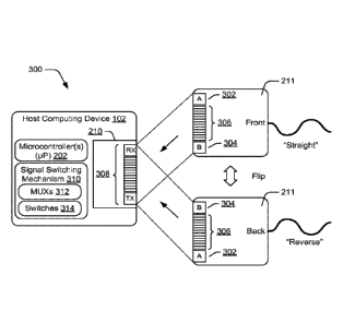
associated with a set of detection cases each of which corresponds to a type
of device and/or
an orientation of a connector 211. Lines associated with the detection pins
may be sampled
together (e.g., in parallel or in sequence) and values for obtained for the
different lines may
be combined together to derive a combined logic state that is indicative of
the device type
and/or connector orientation. Accordingly, a table, file, database or other
data structure may
be established that reflects mapping of logic state combinations (or other
credentials/accessory identifiers) with corresponding detection cases. In
operation, the one
or more microcontrollers 202 may monitor the detection pins and obtain values
on each
detection line. The microcontrollers 202 may make use of a mapping of the
possible logic
state combinations with corresponding detection cases to resolve the device
type and
connector orientation.
[0041] Regarding device type, the logic state combinations provide a mechanism
to
enable the host to distinguish between different types of devices. In
particular, a detected
logic state combination indicates whether a device is a one wire device that
may
communicate via a single line with RX and TX combined or a two wire device
that uses two
different lines for RX and TX One wire devices may be relatively simple and
low cost
devices that do not use complex communication schemes, such as a basic power
adapter or
external battery. Two wire devices may be devices that provide functionality
involving
advanced interfaces, high speed communications, and/or multiple types of
data/protocols,
such as a docking station, multi-media accessory, and so forth.
[0042] In the case of a pair of detection pins allocated for hot plug
detection, such as
HPD1A and HPD1B (e.g., Pin A 302 and Pin B 304), there are four possible logic
state
combinations, e.g., high-high, high-low, low-high, and low-low. The logic
states are
13
CA 02948655 2016-11-09
WO 2015/191790 PCT/US2015/035218
indicative of the type of device (e.g., one wire or two wire) and may also be
used to directly
or indirectly resolve the connector orientation. In particular, both of the
pins HPD1A and
HPD1B are not asserted (e.g., in a low state) in the absence of a connected
accessory. When
an accessory device is connected to the host, the particular combination of
the states for
HPD1A and HPD1B determines the accessory type. For one wire devices, the line
on which
a high state is asserted can be determined. Accordingly, the logic state
combination for a
one-wire device also reflects the connector orientation and may be used
directly to ascertain
the orientation. For two wire devices, both lines have high states and thus
the logic state
combination may be insufficient to resolve the orientation. Therefore,
additional processing
may be performed as described below to ascertain the orientation of a two wire
device.
[0043] Thus, for the detection pins HPD1A and HPD1B, the following shows an
illustrative table showing an example mapping of possible logic state
combinations to
detection cases:
TABLE 1: Detection Pin Logic State Mapping
HPD1A HPD1A
High = 1 Low = 0
HPD1B Two wire accessory One wire accessory
High ¨ 1 (reverse)
HPD1B One wire accessory No accessory attached
Low = 0 (straight)
[0044] Per the above table, the values 1, 1 (high-high) indicates a two wire
accessory, 1,
0 (high-low) indicates a one wire accessory in a straight orientation, 0, 1
(low-high) indicates
a one wire accessory in a reverse orientation, and 0, 0 (low-low) indicates
that no accessory
is attached. After determining the device type using a mapping such as the
example of
Table 1, additional processing may occur to perform
authentication/authorization of device,
determine a particular identity and/or capabilities of the device (as opposed
to just the one
wire vs two wire determination), and set-up switching mechanisms of the host
and/or
accessory to route signals appropriately.
[0045] For example, for a one wire device, sampling may occur via the asserted
pin (either
HPD lA or HPD1B) to identify and authorize the device. This may involve
various different
14
CA 02948655 2016-11-09
WO 2015/191790 PCT/US2015/035218
authentication techniques as described previously. The authentication enables
the
hostimicrocontroller to recognize unsupported accessories and determine
specific
configuration information for supported accessories based on the particular
accessory
identity to configure the interface and signal routing accordingly. For
instance, accessory
devices may be configured to supply credentials 220 to the host in various
ways as
mentioned previously. In one approach, accessory devices are configured to
expose a
respective resistor value indicative of the identity for reading by the host
computing device.
Different resistor values may be associated with different accessories. Thus,
when an
accessory is connected, the host computing device may read a corresponding
resistor value
and distinguish between different accessories on this basis. Alternatively,
other credentials
220 may be communicated to the host by an accessory to indicate its identity,
such as
sending a particular numeric code, an ID field value, a device name, and so
forth.
[0046] As noted, when the attached accessory is a two wire device, the logic
state
combination is not sufficient to enable an orientation determination. In this
case, orientation
is resolved through the authentication sequence. In order to do so, supported
two wire
devices may be configured to supply credentials 220 to the host via either or
both of the
signal lines. In this case, sampling occurs for both of HPD1A or HPD1B to
identify and
authorize the two wire device. In one approach, the two wire device may have
ID resistors
associated with one or both lines and may expose the resistor value(s)
indicative of the
identity. Again, other credentials 220 may also be communicated to the host by
an accessory
to indicate its identity. Orientation may then be determined based on mapping
of ID validity
states for each line, e.g., valid or invalid, to possible orientation cases.
Thus, for the
detection pins HPD IA and HPD1B, the following shows an illustrative table
showing an
example mapping of ID validity states orientation cases:
TABLE 2: Two-Wire Detection Pin ID Validity State Mapping
HPD1A: HPD1A:
valid ID invalid ID
HPD1B: Both orientations 2-wire accessory (reverse)
valid ID supported. Configure based
on application
HPD1B: 2-wire accessory (straight) unsupported
accessory
invalid ID
CA 02948655 2016-11-09
WO 2015/191790 PCT/US2015/035218
[0047] FIG. 6 depicts an example procedure 600 that illustrates example logic
for
processing that may occur to detect both device type and orientation in
accordance with one
or more implementations. In particular, the procedure 600 represents but one
example
technique that may be employed to resolve device type and connector
orientation upon
connection of an accessory to a host. The procedure 600 additionally
represents one possible
implementation of the mappings for detection pins HPD 1 A and HPD reflected in
Table
1 and Table 2 described just above.
[0048] An accessory port is monitored (block 602) to detect connection of an
accessory
via a corresponding connector cord. The monitoring may be implemented by a
.. microcontroller 202 and/or security module 216 as described herein. The
accessory port
210 and connector 211 may be configured to have a pair of pins allocated for
detection, e.g.,
detection pins HPD and HPD1B. A determination is made regarding whether either
of
pins HPD1A and HPD1B is asserted (e.g., signal value of high =1) (block 604).
If not,
monitoring of the port continues per block 602. If at least one of the pins is
asserted, a check
.. is made to determine if both pins are asserted (block 606). If both pins
are not asserted,
procedure 600 proceeds to operations associated with one wire configuration
and otherwise
both pins are asserted and procedure 600 proceeds to operations associated
with two wire
configuration.
[0049] For one wire configuration, determination is made regarding whether HPD
is
asserted (block 608) and if so, HPD1A is sampled (block 610) to obtain
credentials for
identification. Based on the credentials, an ID of the connected accessory is
validated (block
612) and when the ID is valid, the system is configured for one wire in
straight orientation
(block 614). On the other hand, if the ID is not valid the accessory is an
unsupported
accessory (block 616) and interaction may be restricted. If HPD IA is not
asserted per block
608, the other pin HPD1B is the asserted pin and is sampled (block 618). ID
validation
again occurs (block 620) and either, the ID is valid and the system is
configured for one
wire in reverse orientation (block 622) or the ID is not valid the accessory
is an unsupported
accessory (block 616) and may be restricted.
[0050] For two wire configuration, both HPD1A and HPD1B are sampled (block
624).
ID validation occurs for HPD1A (block 626) and then for HPD1B (block 628) if
the ID
sampled on HPD1A is valid. If IDs for both HPD1A and HPD1B are valid, then
both
straight and reverse orientations are supported and configuration occurs based
on the
application (block 630). Otherwise, if just the ID for HPD1A is valid, then
the system is
configured for two wire in straight orientation (block 632). If HPD1A is not
valid per block
16
CA 02948655 2016-11-09
WO 2015/191790 PCT/US2015/035218
626, ID validation occurs for HPD1B (block 634). If HPD1B is valid per block
634, then
system is configured for two wire in reverse orientation (block 636).
Otherwise, IDs
sampled for both HPD1A and HPD1B are invalid and the accessory is an
unsupported
accessory (block 638) and may be restricted. Following configuration of the
system in the
appropriate way based on the depicted logic, signals are the routed using the
configuration
that us applied (block 640).
[0051] Example procedure 600 may be implemented in software, firmware,
hardware, or
a combination of each or some of same. A software or firmware implementation
may be
advantageously flexible and reconfigured with a software or firmware update.
Alternatively, example procedure 600 may be implemented using discrete logic
gates and
analog and mixed-signal circuits, including analog-to-digital circuits. This
alternative may
be advantageously faster and may also comprise programmable thresholds, for
example, for
determining resistor values. Because of the binary nature of the decisions,
digital logic may
be used extensively.
[0052] Having considered the foregoing example procedures, consider now a
discussion
of example systems and devices that may be employed to implement aspects of
reversible
connector techniques in one or more embodiments.
Example System and Device
[0053] FIG. 7 illustrates an example system generally at 700 that includes an
example
computing device 702 that is representative of one or more computing systems
and/or
devices that may implement the various techniques described herein. The
computing device
702 may be, for example, be configured to assume a mobile configuration
through use of a
housing formed and size to be grasped and carried by one or more hands of a
user, illustrated
examples of which include a mobile phone, mobile game and music device, and
tablet
computer although other examples are also contemplated.
[0054] The example computing device 702 as illustrated includes a processing
system 704,
one or more computer-readable media 706, and one or more I/O interface 708
that are
communicatively coupled, one to another. Although not shown, the computing
device 702
may further include a system bus or other data and command transfer system
that couples
the various components, one to another. A system bus can include any one or
combination
of different bus structures, such as a memory bus or memory controller, a
peripheral bus, a
universal serial bus, and/or a processor or local bus that utilizes any of a
variety of bus
architectures. A variety of other examples are also contemplated, such as
control and data
lines.
17
CA 02948655 2016-11-09
WO 2015/191790 PCT/US2015/035218
[0055] The processing system 704 is representative of functionality to perform
one or more
operations using hardware. Accordingly, the processing system 704 is
illustrated as
including hardware element 710 that may be configured as processors,
functional blocks,
and so forth. This may include implementation in hardware as an application
specific
integrated circuit or other logic device formed using one or more
semiconductors. The
hardware elements 710 are not limited by the materials from which they are
formed or the
processing mechanisms employed therein. For example, processors may be
comprised of
semiconductor(s) and/or transistors (e.g., electronic integrated circuits
(ICs)). In such a
context, processor-executable instructions may be electronically-executable
instructions.
[0056] The computer-readable storage media 706 is illustrated as including
memory/storage
712. The memory/storage 712 represents memory/storage capacity associated with
one or
more computer-readable media. The memory/storage component 712 may include
volatile
media (such as random access memory (RAM)) and/or nonvolatile media (such as
read only
memory (ROM), Flash memory, optical disks, magnetic disks, and so forth). The
memory/storage component 712 may include fixed media (e.g., RAM, ROM, a fixed
hard
drive, and so on) as well as removable media (e.g., Flash memory, a removable
hard drive,
an optical disc, and so forth). The computer-readable media 706 may be
configured in a
variety of other ways as further described below.
[0057] Input/output interface(s) 708 are representative of functionality to
allow a user to
enter commands and information to computing device 702, and also allow
information to
be presented to the user and/or other components or devices using various
input/output
devices. Examples of input devices include a keyboard, a cursor control device
(e.g., a
mouse), a microphone, a scanner, touch functionality (e.g., capacitive or
other sensors that
are configured to detect physical touch), a camera (e.g., which may employ
visible or non-
visible wavelengths such as infrared frequencies to recognize movement as
gestures that do
not involve touch), and so forth. Examples of output devices include a display
device (e.g.,
a monitor or projector), speakers, a printer, a network card, tactile-response
device, and so
forth. Thus, the computing device 702 may be configured in a variety of ways
to support
user interaction.
[0058] The computing device 702 is further illustrated as being
communicatively and
physically coupled to an accessory device 714 that is physically and
communicatively
removable from the computing device 702. In this way, a variety of different
input devices
may be coupled to the computing device 702 having a wide variety of
configurations to
support a wide variety of functionality. In this example, the accessory device
714 includes
18
CA 02948655 2016-11-09
WO 2015/191790 PCT/US2015/035218
one or more controls 716, which may be configured as press-sensitive keys,
mechanically
switched keys, buttons, and so forth.
[0059] The accessory device 714 is further illustrated as include one or more
modules 718
that may be configured to support a variety of functionality. The one or more
modules 718,
for instance, may be configured to process analog and/or digital signals
received from the
controls 716 to determine whether an input was intended, determine whether an
input is
indicative of resting pressure, support authentication of the accessory device
714 for
operation with the computing device 702, and so on.
[0060] Various techniques may be described herein in the general context of
software,
hardware elements, or program modules. Generally, such modules include
routines,
programs, objects, elements, components, data structures, and so forth that
perform
particular tasks or implement particular abstract data types. The terms
"module,"
"functionality," and "component" as used herein generally represent software,
firmware,
hardware, or a combination thereof. The features of the techniques described
herein are
platform-independent, meaning that the techniques may be implemented on a
variety of
commercial computing platforms having a variety of processors.
[0061] An implementation of the described modules and techniques may be stored
on or
transmitted across some form of computer-readable media. The computer-readable
media
may include a variety of media that may be accessed by the computing device
702. By way
of example, and not limitation, computer-readable media may include "computer-
readable
storage media" and "computer-readable signal media."
[0062] "Computer-readable storage media" refers to media and/or devices that
enable
storage of information in contrast to mere signal transmission, carrier waves,
or signals per
sc. Thus, computer-readable storage media does not include signals per se or
signal-bearing
media. The computer-readable storage media includes hardware such as volatile
and non-
volatile, removable and non-removable media and/or storage devices implemented
in a
method or technology suitable for storage of information such as computer
readable
instructions, data structures, program modules, logic elements/circuits, or
other data.
Examples of computer-readable storage media may include, but are not limited
to, RAM,
ROM, EEPROM, flash memory or other memory technology, CD-ROM, digital
versatile
disks (DVD) or other optical storage, hard disks, magnetic cassettes, magnetic
tape,
magnetic disk storage or other magnetic storage devices, or other storage
device, tangible
media, or article of manufacture suitable to store the desired information and
which may be
accessed by a computer.
19
CA 02948655 2016-11-09
WO 2015/191790 PCT/US2015/035218
[0063] "Computer-readable signal media" may refer to a signal-bearing medium
that is
configured to transmit instructions to the hardware of the computing device
702, such as via
a network. Signal media typically may embody computer readable instructions,
data
structures, program modules, or other data in a modulated data signal, such as
carrier waves,
data signals, or other transport mechanism. Signal media also include any
information
delivery media. The term "modulated data signal" means a signal that has one
or more of
its characteristics set or changed in such a manner as to encode information
in the signal.
By way of example, and not limitation, communication media include wired media
such as
a wired network or direct-wired connection, and wireless media such as
acoustic, RF,
infrared, and other wireless media.
[0064] As previously described, hardware elements 710 and computer-readable
media 706
are representative of modules, programmable device logic and/or fixed device
logic
implemented in a hardware form that may be employed in some embodiments to
implement
at least some aspects of the techniques described herein, such as to perform
one or more
instructions. Hardware may include components of an integrated circuit or on-
chip system,
microcontroller devices, an application-specific integrated circuit (AS1C), a
field-
programmable gate array (FPGA), a complex programmable logic device (CPLD),
and other
implementations in silicon or other hardware. In this context, hardware may
operate as a
processing device that performs program tasks defined by instructions and/or
logic
embodied by the hardware as well as a hardware utilized to store instructions
for execution,
e.g., the computer-readable storage media described previously.
[0065] Combinations of the foregoing may also be employed to implement various
techniques described herein. Accordingly, software, hardware, or executable
modules may
be implemented as one or more instructions and/or logic embodied on some form
of
computer-readable storage media and/or by one or more hardware elements 710.
The
computing device 702 may be configured to implement particular instructions
and/or
functions corresponding to the software and/or hardware modules. Accordingly,
implementation of a module that is executable by the computing device 702 as
software may
be achieved at least partially in hardware, e.g., through use of computer-
readable storage
media and/or hardware elements 710 of the processing system 704. The
instructions and/or
functions may be executable/operable by one or more articles of manufacture
(for example,
one or more computing devices 702 and/or processing systems 704) to implement
techniques, modules, and examples described herein.
CA 02948655 2016-11-09
WO 2015/191790 PCT/US2015/035218
Conclusion
[0066] Although the example implementations have been described in language
specific to
structural features and/or methodological acts, it is to be understood that
the
implementations defined in the appended claims is not necessarily limited to
the specific
features or acts described. Rather, the specific features and acts are
disclosed as example
forms of implementing the claimed features.
21