Note: Descriptions are shown in the official language in which they were submitted.
METHODS AND SYSTEMS FOR THE SYNTHESIS OF NANOPARTICLES INCLUDING
STRAINED NANOPARTICLES
BACKGROUND
[0002] Nanoparticles have been of much interest in a variety of
applications from solar cells to diagnostic medicines to transistors. While
the
commercial applications of oxide nanoparticles are prevalent, e.g., nano-
titania
and nano-silica in sunscreens and nano-iron oxide in biomedical imaging, metal
nanoparticles and nanocrystals applications have lagged behind. One
significant
barrier to the wide-spread implementation of metal nanoparticles and
nanocrystals has been the production of commercial-scale qualities with
specific
physical properties. This is especially true for nanocrystals as their
applications
often prefer, if not require, high uniformity (e.g., narrow size distributions
and
consistent shapes).
[0003] This high uniformity is difficult to achieve with the more
prevalent synthesis routes like laser ablation, sputtering, and some wet-
chemistry methods. While some wet-chemistry methods can meet the narrow
size distribution requirement, the large volumes of chemicals, especially
solvents, required to produce the nanoparticle and the longer synthesis time
significantly increase the cost and environmental impact, which in turn
hinders
scale-up efforts.
SUMMARY
[0004] The present disclosure relates to methods and systems for the
synthesis of nanoparticles, including unique nanoparticles produced with such
methods and systems.
[0005] According to one embodiment, a method for synthesizing
nanoparticles is disclosed. The method may include aerosolizing a precursor
solution in the presence of a flowing carrier gas to yield a reactant stream,
the
precursor solution comprising a volatile solvent and a nanoparticle precursor.
The method may further include heating the reactant stream to a temperature
above a boiling point of the volatile solvent to form a product stream
comprising
a plurality of nanoparticles, cooling the product stream, and passing the
product
stream through a collection liquid to collect the nanoparticles from the
product
stream.
1
CA 2949102 2018-07-19
[0005a]
According to one embodiment a method for continuous
manufacture of nanoparticles comprising aerosolizing a precursor solution
using
a sonicator at a frequency between 1 kHz and 200 kHz in the presence of a
flowing carrier gas to yield a reactant stream, the precursor solution
comprising
a volatile solvent and a nanoparticle precursor comprising a Group IV
elemental
compound;
flowing the reactant stream through a first reaction zone;
heating the reactant stream within the first reaction zone to a first
temperature above a boiling point of the volatile solvent;
flowing the reactant stream through a second reaction zone;
heating the reactant stream in the second reaction zone at a second
temperature to form a product stream comprising a plurality of nanoparticles;
flowing the reactant stream through a third reaction zone;
cooling the product stream in the third reaction zone at a third
temperature, wherein
the first temperature is not greater than the second temperature and the
third temperature is less than each of the first and second temperatures; and
passing the product stream through a collection liquid to collect the
nanoparticles from the product stream.
la
CA 2949102 2019-02-20
CA 02949102 2016-11-14
WO 2015/176045 PCT/US2015/031255
[0006] According to another embodiment, a method of synthesizing
nanoparticles
is disclosed. The method may include continuously aerosolizing a precursor
solution in the
presence of a flowing carrier gas to yield a reactant stream, the precursor
solution
comprising a volatile solvent and a nanoparticle precursor. The method may
further include
continuously replenishing the precursor solution, heating the reactant stream
to a
temperature above a boiling point of the volatile solvent to form a product
stream comprising
a plurality of nanoparticles, cooling the product stream. The method may
further include
passing the product stream through a collection liquid to collect the
nanoparticles from the
product stream and continuously replacing the collection liquid.
[0007] According to yet another embodiment, a nanoparticle is disclosed,
the
nanoparticle including a Group IV element and having a shifted crystal plane
peak.
[0008] According to yet another embodiment, a system for synthesizing
nanoparticles is disclosed. The system may include a precursor solution vessel
configured to
contain a precursor solution including a volatile solvent and a nanoparticle
precursor and
receive a carrier gas. The system may further include an aerosolizing device
for to
aerosolizing the precursor solution. The system may further include a tube
furnace
configured to transport and heat a reactant stream comprising the aerosolized
precursor
solution and the carrier gas to produce nanoparticles. The system may further
include a
collection vessel containing a collection liquid for collecting the
nanoparticles.
[0009] The features and advantages of the various embodiments will be
readily
apparent to those skilled in the art upon a reading of the description of the
preferred
embodiments that follows.
BRIEF DESCRIPTION OF THE DRAWINGS
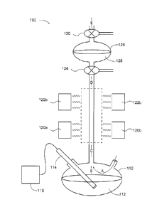
[0010] FIG. 1 is a system for producing nanoparticles.
[0011] FIG. 2 is a system for producing nanoparticles.
[0012] FIG. 3 is a process chart illustrating the fabrication of one or
more devices
that comprise nanoparticles.
[0013] FIG. 4 is a diagram illustrating the layers of a coated substrate
comprising
nanoparticles.
[0014] FIG. 5 is a scanning electron micrograph of a layer of smaller (9
nm)
silicon nanocrystals deposited over a layer of larger (25 nm) silicon
nanocrystals.
[0015] FIG. 6 is a diagram illustrating layers of a coated substrate
comprising
nanoparticles.
[0016] FIG. 7 is a diagram illustrating layers of a coated substrate
comprising
nanoparticles.
2
CA 02949102 2016-11-14
WO 2015/176045
PCT/US2015/031255
DETAILED DESCRIPTION
[0017] The present disclosure relates to methods and systems for
the synthesis
of nanoparticles, including unique nanoparticles produced with such methods
and systems.
[0018] The methods and systems of the present disclosure may
advantageously
enable the high-yield production of nanoparticles (e.g., 85% or greater yield
in some
embodiments), and especially nanocrystals and metal nanoparticles, with narrow
size
distributions (e.g., about 2 nm in some embodiments). Further, the methods
and systems
described herein are capable of being adapted to relatively high-production
rates (e.g.,
kilograms per hour) and continuous methods, which may enable industrial-scale
production
of highly uniform nanoparticles, including nanocrystals and metal
nanoparticles.
[0019] In addition, the methods and systems described herein have
been
unexpectedly found to, in some embodiments, yield unique nanoparticle
compositions, which
may be useful in a plurality of applications including ion batteries and
quantum energy
devices.
[0020] It should be noted that when "about" is used herein at the beginning
of a
numerical list, "about" modifies each number of the numerical list. It should
be noted that in
some numerical listings of ranges, some lower limits listed may be greater
than some upper
limits listed. One skilled in the art will recognize that the selected subset
will require the
selection of an upper limit in excess of the selected lower limit.
I. Methods and Systems for Producing Nanoparticles
[0021] Various embodiments described herein may involve producing
nanoparticles by heating an aerosolized precursor solution, which in some
embodiments
may be adapted for continuous and high-production rate nanoparticle
production.
[0022] Some embodiments may involve aerosolizing a precursor
solution in the
presence of a flowing carrier gas, thereby yielding a reactant stream; heating
the reactant
stream to form a product stream that comprises a plurality of nanoparticles;
cooling the
product stream; and passing the product stream through a liquid to collect the
nanoparticles
from the product stream. In some embodiments, the precursor solution may
comprise a
volatile solvent and nanoparticle precursors; and the reactant stream may be
heated to a
temperature above the boiling point of the volatile solvent. As used herein,
the term
"nanoparticle" refers to particles having at least one dimension less than
about 40 m and
encompasses amorphous nanoparticles, nanocrystals, core-shell nanoparticles,
non-
spherical nanoparticles (e.g., oblong or rod-like particles), substantially
spherical
nanoparticles, hollow spherical nanoparticles, and the like.
[0023] Aerosolizing the precursor solution forms droplets that, when heated
above the boiling point of the volatile solvent, may cause the volatile
solvent to evaporate
from the droplet and the nanoparticle precursors droplets to coalesce and
react, thereby
3
CA 02949102 2016-11-14
WO 2015/176045
PCT/US2015/031255
yielding nanoparticles, and in some instances nanocrystals. It should be noted
that
depending on the conditions of synthesis (e.g., aerosolizing parameters,
reaction
temperatures, volatile solvent composition, and nanoparticle precursor
compositions and/or
concentrations) nanoparticles may be formed by a one droplet-one nanoparticle
mechanism,
a ripening mechanism, a disintegration mechanism, or a combination thereof. In
various
embodiments, the one droplet-one nanoparticle mechanism may produce
monodispersed
particles (i.e., single size particles). In other embodiments, the
disintegration mechanism
may produce bimodal, trimodal, or other multi-modal nanoparticle size
distributions. Such
multimodal distributions of nanoparticles may enable higher packing efficiency
when
deposited in a layer on a substrate.
[0024] Referring now to FIG. 1, a system for producing
nanoparticles, generally
designated 100, is shown. The system 100 may include a precursor solution
vessel 110 that
contains a precursor solution 112, which has submersed therein a sonicator 114
for
producing an aerosol B. The sonicator 114 may be attached to a control box 116
that
enables manipulation of the frequency, amplitude, and waveform produced by the
sonicator
114. Further, the precursor solution vessel 110 has a carrier gas A passing
though it, which
mixes with the aerosol B to yield a reactant stream C. The reactant stream C
may pass
through a reaction zone 118 where the reactant stream C is heated by heaters
120a,b and
122a,b to yield a product stream D comprising nanoparticles. The heaters 120a,
b and 122
a, b may be adjusted to form different zones in the reaction zone C having
different zone
temperatures. The product stream D is then passed through a collection liquid
128 in a
collection vessel 126 where the nanoparticles are at least substantially
removed from the
product stream D to yield an effluent stream E. As shown here, three-way
valves 124 and
130 are used to control the pressure and gas flow rates through the collection
vessel 126 so
as to prevent the collection liquid 128 from flowing back into the reaction
zone 118. It should
be noted that other mechanism like vacuum and additional carrier gases
introduced above
the reaction zone may also be utilized to assist in preventing the collection
liquid 128 from
flowing back into the reaction zone 118.
[0025] In some embodiments, precursor solutions may comprise a
volatile
solvent and a nanoparticle precursor.
[0026] Volatile solvents may, in some embodiments, be organic
solvents having
a boiling point of about 300 C or less. Examples of volatile solvents suitable
for use in
conjunction with the methods described herein may include, but are not limited
to alcohols
(e.g., methanol, ethanol, isopropanol, and butantol), glycols, acetonitrile,
water, and the like,
any derivative thereof, and any combination thereof. Anhydrous precursor
solvents may be
used to minimize oxidation of the final product. The solvent may be selected,
for example,
based on the dielectric constant of the solvent. In various embodiments, the
dielectric
4
CA 02949102 2016-11-14
WO 2015/176045 PCT/US2015/031255
constant of the solvent may be matched to the dielectric constant of
organometallic
precursors. In other embodiments, the solvent may be selected based on its
miscibility. For
example, in certain embodiments, it may be desirable to create an emulsion for
use as
precursor as opposed to solvents miscible with precursor that creates a
solution.
[0027] Nanoparticle precursors may, in some embodiments, be organometallic
compounds. Nanoparticle precursers may include silicon chloride, germanium
chloride, etc.
Nanoparticle precursors may comprises transition elements (e.g., titanium,
chromium, iron,
cobalt, nickel, copper, zinc, molybdenum, palladium, silver, cadmium,
tungsten, platinum,
and gold), lanthanide elements (e.g., europium, gadolinium, and erbium), Group
HI elements
(boron, aluminum, gallium, indium, and thallium), Group IV elements (e.g.,
germanium,
silicon, tin, lead, and carbon), Group V elements (e.g., nitrogen,
phosphorous, arsenic,
antimony, and bismuth), Group VI elements (e.g., oxygen, sulfur, selenium, and
tellurium), or
any combination thereof. Examples of nanoparticles precursors suitable for use
in
conjunction with the methods described herein may, in some embodiments,
include, but are
not limited to, tetraethylgermane, tetramethylgermane, tetraethylsilane,
tetramethylsilane,
diethylsilane, diethylgermane, diethyl silane, tetrapropyl germane,
tetrapropyl silane and the
like, any derivative thereof, or any combination thereof.
[0028] In some embodiments, more than one nanoparticle precursor
may be
utilized in the precursor solutions described herein. For example, a precursor
solution may
comprise a first nanoparticle precursor that includes germanium and a second
nanoparticle
precursor that includes silicon. In some embodiments, precursor solutions may
comprise
more than one nanoparticle precursor such that the mole ratio of the metal of
the first
nanoparticle precursor (e.g., germanium) to the metal of the second
nanoparticle precursor
(e.g., silicon) ranges from a lower limit of about 1:10, 1:5, or 1:1 to an
upper limit of about
10:1, 5:1, or 1:1, and wherein the mole ratio may range from any lower limit
to any upper
limit and encompasses any subset therebetween. In other embodiments, when
multimodal
distributions are desired, pure organometallic precursors may be used in
accordance with a
droplet disintegration mechanism. One skilled in the art with the benefit of
this disclosure
should understand that the germanium and silicon example is nonlimiting and
other
combinations of nanoparticle precursors may be applicable, e.g., cadmium and
selenium, tin
and tellurium, and zinc and sulfur.
[0029] In some embodiments, the nanoparticle precursors may be
present in the
precursor solutions described herein in an amount ranging from a lower limit
of about 20%,
30%, 40%, or 50% by volume of the precursor solution to an upper limit of
about 90%, 70%,
50%, or 40% by volume of the precursor solution, and wherein the amount may
range from
any lower limit to any upper limit and encompasses any subset therebetween.
5
CA 02949102 2016-11-14
WO 2015/176045 PCT/US2015/031255
[0030] In some embodiments, aerosolizing the precursor solution may
involve at
least one of sonicating the precursor solution with the sonication probe
immersed in the
precursor solution (e.g., as shown in FIG. 1), nebulizing the precursor
solution, passing the
precursor solution through a nozzle (e.g., an aerosolizing nozzle),
electrostatic precipitation,
and the like, and any combination thereof.
[0031] In some embodiments, aerosolizing the precursor solution,
including by
any method described herein, may be performed at a frequency ranging from a
lower limit of
about 1 kHz, 10 kHz, 100 kHz, 1 MHz, 10 MHz, or 100 MHz to an upper limit of
about 1000
MHz, 100 MHz, 10 MHz, 1 MHz, or 100 kHz, and wherein the frequency may range
from any
lower limit to any upper limit and encompasses any subset therebetween (e.g.,
3 kHz to 150
kHz). In some embodiments, aerosolizing the precursor solution, including by
any method
described herein, may be performed at a frequency so as to yield strained
nanoparticles
(described further herein), which may be a frequency ranging from a lower
limit of about 1
kHz, 3 kHz, 10 kHz, or 15 kHz to an upper limit of about 200 kHz, 150 kHz, 50
kHz, or 25
kHz, and wherein the frequency may range from any lower limit to any upper
limit and
encompasses any subset therebetween, e.g., 5 kHz to 22 kHz.
[0032] In some embodiments, aerosolizing the precursor solution,
including by
any method described herein, may be performed at an input power ranging from a
lower limit
of about 10 Watts (or a frequency of about 5kHz) to an upper limit of about
100 Watts (or a
frequency of about 22kHz), and wherein the input power may range from any
lower limit to
any upper limit and encompasses any subset therebetween. Those skilled in the
art will
appreciate that additional factors relating to energy supplied to the system
may also affect
the physical properties of the resulting nanoparticles, such as the internal
strain. Additional
factors may include waveform, amplitude, heat, or any other additional energy
added into the
system when forming droplets at input.
[0033] In some embodiments, the aerosolized precursor solution B
may be mixed
with a carrier gas A to form a reactant stream C. The carrier gas A may
transport the
aerosolized precursor solution through the reaction zone 118. Further the flow
rate of the
carrier gas A may be adjusted to provide for a desired residence time of the
reactant stream
C in the reaction zone 118. In some embodiments, the residence time of the
reactant stream
C in the reaction zone 118 may range from a lower limit of about 1 sec to an
upper limit of
about 10 sec.
[0034] In some embodiments, the carrier gas A may be an inert gas
(e.g.,
helium). In other embodiments, the carrier gas A may not be inert (e.g.,
hydrogen).
Examples of carrier gases suitable for use in conjunction with the methods
described herein
may, in some embodiments, include, but are not limited to, hydrogen, helium,
nitrogen,
argon, carbon dioxide, and the like, and any combination thereof.
6
CA 02949102 2016-11-14
WO 2015/176045 PCT/US2015/031255
[0035] In some embodiments, the reactant stream C may be heated to
a
temperature above the boiling point of the volatile solvent so as to form a
product stream D
that comprises a plurality of nanoparticles. In some embodiments, the
temperature above
the boiling point of the volatile solvent may range from a lower limit of
about 500 C, 600 C,
or 700 C to an upper limit of about 1200 C, 1100 C, 1000 C, or 900 C, and
wherein the
temperature may range from any lower limit to any upper limit and encompasses
any subset
therebetween.
[0036] In some embodiments, heating may involve passing the
reactant stream C
through a tube furnace, series of tube furnaces, or the like. Without being
limited by theory, it
is believed that nanoparticle precursors and/or nanoparticles may collect on
the walls of the
tube passing through the tube furnace, thereby decreasing the overall yield of
nanoparticles
produced. Various embodiments may minimize interaction between the walls and
the
reactant stream. Minimizing such interactions may, in some embodiments,
involve at least
one of orienting the tube furnace vertically, spinning the tube through which
the reactant
stream is passing, applying an electric charge to the tube, providing sheath
flow within the
tube furnace (e.g., flowing a sheath of a gas between the tube wall and the
reactant stream),
creating a vortex within the reactant stream (e.g., with a spinning or
oscillating rod or the like
extending into the reaction zone), using a tapered tube in conjunction with a
cortex, and the
like, any hybrid thereof, and any combination thereof.
[0037] Some embodiments may pass the product stream D through the
collection
liquid 128 so as to collect the nanoparticles therein. The collection liquid
128 may, in some
embodiments, be solvents suitable for use in applications downstream of
nanoparticle
production (e.g., deposition on surfaces, compounding with polymers, chemical
modification,
and the like). Examples of the collection liquid 128 suitable for use in
collecting nanoparticles
produced by the methods and systems described herein may include methanol,
ethanol,
glycol, water, tetrahydrofuran (THF), diethylcarbonate, acetonitrile,
dichlorobenzene,
acetone, toluene, pentane and the like, any derivative thereof, or any
combination thereof.
[0038] In some embodiments, the collection liquid 128 may further
comprise
suspension agents, which may, in some embodiments, assistant suspension of the
nanoparticles and/or mitigate clustering of the nanoparticles. In some
embodiments,
suspension aids may covalently or noncovalently interact with the
nanoparticles. Examples
of suspension agents suitable for use in conjunction with the production of
nanoparticles
described herein may include surfactants, polymers, chelating agents, capping
agents (e.g.,
octanol, oleylamine, and trioctylamine), and the like, or any combination
thereof.
[0039] In some embodiments, the path that the product stream C follows from
the
reaction zone to the collection liquid 128 may be substantially straight
(e.g., containing a
bend or deviation of about 30 or less) and/or substantially vertical (e.g.,
about 30 or less
7
CA 02949102 2016-11-14
WO 2015/176045 PCT/US2015/031255
off-vertical) to minimize the collection of nanoparticle precursors and/or
nanoparticles on
surfaces, thereby increasing the yield of nanoparticles. In some embodiments,
the yield of
nanoparticles may be about 65% or greater, about 75% or greater, or more
preferably about
85% or greater (e.g., about 85% to about 90%) by weight of the metal of the
nanoparticle
precursor relative to the metal of the nanoparticle produced.
[0040] In some embodiments, the methods and systems described
herein may
be adapted for continuous and high-production rate nanoparticle production.
Referring now
to FIG. 2, a system for producing nanoparticles, generally designated 200, is
shown. The
system 200 may include precursor solution vessel 210 that contains precursor
solution 212.
The precursor solution 212 may be in contact with an apparatus 214, e.g., a
large-scale
mister or fogger, capable of producing large volumes of aerosolized precursor
solution B. To
enable a continuous process, system 200 may include syringe pump 232 (or
another similar
automated addition system) for continuous addition of precursor solution 212.
[0041] Precursor solution vessel 210 has passing through it a
carrier gas A,
which mixes with an aerosol B to yield a reactant stream C. The reactant
stream C may pass
through a reaction zone 218 where the reactant stream C is heated by heaters
220a,b to
yield a product stream D that comprises nanoparticles. It should be noted that
the reaction
zone 218 may comprise a single large diameter tube or the like as illustrated
in FIG. 2 or
several smaller tubes or the like in parallel to accommodate the larger
processing volumes
associated with the use of the solution vessel 212. The product stream D is
then passed
through a collection liquid 228 in a collection vessel 226 where the
nanoparticles are at least
substantially removed from the product stream D to yield an effluent stream E.
As shown,
the collection vessel 226 may comprise an inlet 234 and an outlet 236 for
continuous flow of
the collection liquid 228 to enable continuous extraction of the nanoparticles
produced in this
or a similar process.
[0042] As used herein, the term "continuous" refers to being
without interruption
for a prolonged time frame (e.g., about 3 hours or greater). It should be
noted that
continuous actions may be performed intermittently over the short-term (e.g.,
seconds to
minutes) and still be considered continuous over the long term. For example,
continuous
addition of precursor solutions may include the intermittent addition of
precursor solutions
over a prolonged time frame, e.g., the addition of about 1 mL of precursor
solution every 15
minutes.
[0043] Some embodiments may continuously aerosolize a precursor
solution 212
in the presence of a flowing carrier gas A, thereby yielding a reactant stream
C; continuously
replenishing the precursor solution 212; heating the reactant stream C to a
temperature
above a boiling point of the volatile solvent so as to form a product stream D
that comprises
8
CA 02949102 2016-11-14
WO 2015/176045
PCT/US2015/031255
a plurality of nanoparticles; cooling the product stream D; and passing the
product stream D
through a collection liquid 228 so as to collect the nanoparticles from the
product stream.
[0044] Some embodiments may further involve continuously replacing
the
collection liquid 228, e.g., when the nanoparticles have reached a desired
concentration
therein.
[0045] Some embodiments may further involve extracting the
nanoparticles from
the collection liquid 228 (e.g., continuously or batchwise). In some
embodiments, extracting
the nanoparticles from the collection liquid 228 may involve centrifuging,
continuous
centrifuging (e.g., flow centrifugation), filtering, concentrating the
nanoparticles, decanting
the collection liquid after having allowed the nanoparticles to settle, and
the like, and any
hybrid thereof
Nanoparticles
[0046] In some embodiments, the methods and systems described
herein may
form unstrained nanoparticles and/or strained nanoparticles. For example, in a
bimodal
distribution larger nanoparticles may form having strain, while smaller
nanoparticles may
have negligible strain. As used herein, the term "strained nanoparticles"
refers to
nanoparticles having a strained crystal structure, which can be determined by
a shift in a
crystal plane when analyzed by x-ray diffraction ("XRD"). In some embodiments,
the strained
nanoparticles may be nanocrystals, core-shell nanoparticles with a crystalline
core and an
amorphous shell, SiGe core shell nanoparticles, and the like. It should be
noted that, unless
otherwise specified, the term "nanoparticle" encompasses both unstrained
nanoparticles and
strained nanoparticles.
[0047] Without being limited by theory, it is believed that the
frequency of
aerosolization, the amplitude of aerosolization, residence time in the
reaction zone, and
temperature affect the degree of strain, diameter distribution, and/or the
morphology of the
nanoparticle formed by the systems and processes described herein. For
example, the use
of higher frequencies during aerosolization may yield larger nanoparticles. In
another
example, the use of higher amplitudes during aerosolization may yield
nanoparticles with
higher strain.
[0048] The nanoparticles (strained or unstrained) may comprise the metal(s)
of
the nanoparticle precursor(s) used in the production of the nanoparticles. For
example, the
methods and systems described herein may utilize a precursor solution
comprising cadmium
and selenium may yield cadmium selenide nanoparticles. In another example, the
methods
and systems described herein may utilize a precursor solution comprising gold,
platinum, or
palladium so as to yield gold, platinum, or palladium nanoparticles. In yet
another example,
methods and systems described herein may utilize a precursor solution
comprising
9
CA 02949102 2016-11-14
WO 2015/176045 PCT/US2015/031255
germanium and silicon in a desired ratio so as to yield nanoparticles
comprising germanium
and silicon at about the desired ratio.
[0049] Strained nanoparticles may, in some embodiments, comprise
Group III,
Group IV, Group V, and/or Group VI elements. For example, a strained silicon
nanoparticle
may have a 20 value for the (111) crystal plane shifted by about 4 to about 6
from the
(111) crystal plane of bulk silicon. In some embodiments, the 28 value for the
(111) crystal
plane of the strained nanoparticles may shift relative to the corresponding
bulk material from
a lower limit of about 1 , 2 , or 3 , or 4 to an upper limit of about 8 , 7 ,
6 , 5 , or 4 , and
where the shift may range from any lower limit to any upper limit and
encompasses any
subset therebetween.
[0050] In some embodiments, the strained nanoparticles may comprise
Group IV
elements (e.g., germanium, silicon, tin, lead, carbon, or any combination
thereof). In other
embodiments, the strained nanoparticles may comprise a mole ratio of silicon
to germanium
that ranges from a lower limit of about 1:10, 1:5, or 1:1 to an upper limit of
about 10:1, 5:1, or
1:1, and wherein the mole ratio may range from any lower limit to any upper
limit and
encompasses any subset therebetween.
[0051] In some embodiments, the nanoparticles (strained or
unstrained)
described herein may have an average diameter in at least one dimension
ranging from a
lower limit of about 3 nm, 5 nm, 10 nm, 25 nm, or 100 nm to an upper limit of
about 1000
nm, 500 nm, 250 nm, 150 nm, 100 nm, or 50 nm, and wherein the average diameter
in at
least one dimension may range from any lower limit to any upper limit and
encompasses any
subset therebetween.
[0052] In some embodiments, the nanoparticles (strained or
unstrained)
described herein may have a narrow diameter distribution such that the
standard deviation
from the average diameter ranges from a lower limit of about 0.5 nm, 1 nm,
or 2 nm to an
upper limit of about 10 nm, 7 nm, or 5 nm, and wherein the standard
deviation may range
from any lower limit to any upper limit and encompasses any subset
therebetween.
[0053] In some embodiments, the nanoparticles (strained or
unstrained)
described herein may have a multimodal diameter distribution (e.g., bimodal,
trimodal, and
so on). In some embodiments, the nanoparticles (strained or unstrained)
described herein
having a multimodal diameter distribution may have at least one mode with an
average
diameter in at least one dimension ranging from a lower limit of about 4 nm, 7
nm, 12 nm, or
25 nm, to an upper limit of about 250 nm, 150 nm, 100 nm, or 50 nm, and
wherein the
average diameter in at least one dimension may range from any lower limit to
any upper limit
and encompasses any subset therebetween.
[0054] In some embodiments, the modes of a multimodal diameter
distribution of
the nanoparticles (strained or unstrained) described herein may independently
have a
CA 02949102 2016-11-14
WO 2015/176045 PCT/US2015/031255
narrow diameter distribution such that the standard deviation for each mode
independently
ranges from a lower limit of about 0.5 nm, 1 nm, or 2 nm to an upper limit
of about 10
nm, 7 nm, or 5 nm, and wherein the standard deviation may range from any lower
limit to
any upper limit and encompasses any subset therebetween.
[0055] In some embodiments, the nanoparticles may produce
photoluminescence based on the size of the nanoparticles. When the physical
size of a
particle is less than its exciton radius (i.e., physical distance an electron
must travel from its
valence band to conduction band), the quantum phenomenon of photoluminescence
can be
observed. For example, the exciton radius of silicon is 24nm. That is, an
electron must
travel 24nm from its valence band to the conduction band. However, various
embodiments
may produce silicon particles that are less than 24nm, (e.g., it is possible
to synthesize 5nm
silicon particles). In such embodiments, when a photon of sufficient energy
(i.e., ultraviolet
light or, more specifically, a photon greater than the band gap energy of the
nanoscale
material) is absorbed by the nanoparticle, an electron is excited from the
valence band to the
conduction band. The electron may then fall back into the valence band and
emit a photon of
light at a wavelength based on the difference between the particle size and
the exciton
radius. In the case of 5nm silicon, it is blue light. As the physical size of
the particle
approaches the exciton radius, photoluminescence is no longer observed and the
material
begins to behave as a bulk material.
[0056] In various embodiments, the diameter of the nanoparticles may be
determined based on the relationship
Dp 010-0 66(Q)0 207(y)0 11( )0.274( 0 166
) (power/area) 4
Where Dp is the diameter of the resulting particles, a is a constant which
depends on
temperature and choice of precursor solution, f is the transducer/sonicating
frequency, Q is
the flow rate of the carrier gas, Y is the surface tension of the precursor, p
is the density of
the precursor, n is viscosity of the precursor, and power/area is the power
density.
Piezoelectric Effects of Strained Nanoparticles
[0057] In some embodiments, the strained nanoparticles may exhibit
piezoelectric effects. Piezoelectricity is the special circumstance of
electrical charge build-up
that arises in certain solid material structures due to mechanical stress.
Generally, the
piezoelectric effect has been experimentally determined to be a linear
electromechanical
interaction between the mechanical and the electrical state in crystalline
materials with no
inversion symmetry. The piezoelectric effect is a reversible process such that
the internal
generation of electrical charge resulting from an applied mechanical force can
be reversed
with the internal generation of a mechanical strain resulting from an applied
electrical field.
11
CA 02949102 2016-11-14
WO 2015/176045 PCT/US2015/031255
[0058] Regarding the piezoelectric effect in bulk semiconductors,
changes in
inter-atomic spacing resulting from strain affects the semiconductors
intrinsic band gap
making it easier (or harder depending on the material and strain) for
electrons to be raised
into the conduction band. The piezoelectric effect of semiconductor materials
can be several
orders of magnitudes larger than the analogous geometrical effect in metals
and is present
in materials like germanium, polycrystalline silicon, amorphous silicon,
silicon carbide, and
single crystal silicon.
[0059] The piezoelectric effects of semiconductors have been used
for sensor
devices with a variety of semiconductor materials such as germanium,
polycrystalline silicon,
amorphous silicon, and single crystal silicon. Since silicon is currently the
material of choice
for nearly all integrated circuits, the use of piezoelectric silicon devices
has been an intense
area of research interest.
[0060] Regarding the piezoresistive effect in bulk single crystal
silicon and
germanium, the resistance of silicon and germanium can change due to a stress-
induced
change of geometry, but also due to the stress dependent resistivity of the
material. The
resistance of n type silicon (predominant charge carriers responsible for
electrical conduction
are electrons) mainly changes due to a shift of the three different conducting
vertices of the
crystal. The shifting causes a redistribution of the carriers between vertices
with different
mobilities. This results in varying mobilities dependent on the direction of
current flow. A
minor effect is due to the effective mass change related to shape distortion
due to change in
the inter-atomic spacing of valley vertices in single crystal silicon. In p-
type silicon
(predominant charge carriers responsible for electrical conduction are holes)
the phenomena
currently being researched are more complex and also demonstrate changes in
mass and
hole transfer.
[0061] Regarding the piezoelectric mechanism, the nature of the
piezoelectric
effect is rooted in the occurrence of electric dipole moments in solids. An
electric dipole
moment is a vector quantity equal to the product of the magnitude of charge
and the
distance of separation between the charges. Electric dipole moments in solids
may either be
induced for ions on crystal lattice sites as in an asymmetric charge
environment such as in
lithium tantalate and lead zirconate-titanate or may be directly carried by
molecular groups
such as in organic sugar molecules. The dipole density causing polarization is
the sum of the
dipole moments per unit volume of a crystal unit cell. Since electric dipoles
are vector
quantities (geometric objects of specific magnitude and direction), the dipole
density P is
also a vector quantity. Dipoles near each other tend to be aligned in regions
called Weiss
domains. In these aligned regions occurring between individual particles, the
particles act as
a whole. Thus, the potential and polarity of voltage and magnitude and
direction of the
current is equal to the sum of all individual particles making up the entire
solid.
12
CA 02949102 2016-11-14
WO 2015/176045 PCT/US2015/031255
[0062] To reiterate, typically the piezoelectric effect occurs with
an applied
mechanical stress but can also be manifested by manufacturing internal stress
into certain
solids. Piezoelectricity arises because of variation of the polarization
strength, direction, or
both. The magnitude and direction of the charge depends on the
interrelationships between
the orientation of its dipole density P within individual particles, particle
symmetry, and the
applied mechanical stress or induced internal stress. Although the change in
an individual
crystal's dipole density appears quantitatively as a variation of surface
charge density upon
the individual crystal faces, the overall useful energy arising from the
piezoelectric
phenomenon is caused by the superposition of the dipole densities of the
crystals that make
up the entire piece of material, i.e., as a sum of the individual
crystallographic unit cells that
make up a whole crystal. For example, a 1 cm3 cube of quartz with 500 lb of
mechanically
applied force at the right point can produce a voltage of about 12500 V
because the resultant
force is the sum of all the individual crystallographic unit cells that make
up the whole crystal.
[0063] Regarding power generation in bulk polar crystal structures
synthesized in
a state of stress, there are 32 crystal classes that represent 32 possible
combinations of
symmetry operations in crystalline materials. Each crystal class includes
crystal faces that
uniquely define the symmetry of the class. Of the thirty-two crystal classes,
twenty-one are
non-centrosymmetric (not having a centre of symmetry), and of these, twenty
exhibit direct
piezoelectricity. Ten of these include the polar crystal classes, which show a
spontaneous
polarization without an applied mechanical stress due to a non-vanishing
electric dipole
moment associated with asymmetry inherent in their crystal structure. For
polar crystals, for
which the summation of the dipole density P 0 0 holds without applying a
mechanical load,
the piezoelectric effect manifests itself by changing the magnitude or the
direction of P or
both. Stated another way, polar crystals that can be manufactured to have
internal stress will
.. demonstrate a piezoelectric effect without an applied mechanical load.
[0064] Restated another way, for non-polar piezoelectric crystals,
an applied
mechanical load transforms the material from a non-polar crystal class (P = 0)
to a polar
one, having P 0 0 and hence gives rise to a voltage potential and useful
energy capable of
powering an external device. However, crystals predisposed to an internal
state of stress
have an inherent polar structure for which P 0 0 and hence energy can be
discharged from
the structure without an applied mechanical load. During discharge of
electrical energy, the
crystal relaxes back into its preferred state of interatomic spacing.
[0065] In various embodiments, producing strained nanocrystals
depends on a
variety of factors including, for example, the composition of the
nanocrystals, the
temperature(s) of the reaction zone(s), the frequency and power of the
sonicator/mister/fogger/transducer, among other factors. In one embodiment,
strained Si
nanocrystals may be produced in a three stage reaction zone, where the three
stages have
13
CA 02949102 2016-11-14
WO 2015/176045
PCT/US2015/031255
temperatures of 850 C, 850 C, and 650 C, and the power supplied by the
sonicator is
greater than 175W and less than 700W. In another embodiment, strained
germanium
nanocrystals may be produced in a three stage reaction zone, where the three
stages have
temperatures of 750 C, 750 C, and 550 C, and the power supplied by the
sonicator is
greater than 462W and less then 700W. In yet another embodiment, SiGe
nanocrystals may
be produced in a three stage reaction zone, where the three stages have
temperatures of
800 C, 800 C, and 575 C, and the power supplied by the sonicator is greater
than 390W
and less than 700W.
[0066] In addition to producing strained nanoparticles, various
embodiments
enable production of quantum confined nanoparticles, which allows for
increased energy
density in a quantum energy device (QED) produced with the nanoparticles.
Quantum
confinement in nanocrystals occurs when the physical size of the particle is
less than its
characteristic exciton Bohr radius. The exciton Bohr radius is the physical
distance
separating a negatively charged electron from its positively charged hole left
behind during
excitation. When the physical size of the particle is less than the distance
the electron must
travel during excitation, the material is considered to be quantum confined.
For example, the
exciton Bohr radius for germanium is 24.3 nm; however, it is possible to
synthesize
germanium nanocrystals to be 1 nanometer in diameter. By creating
nanoparticles smaller
than this characteristic distance, the electronic properties of the
nanoparticles can be tuned
to discreet energy levels by adjusting particle size. Thus, an aggregate made
of particles
smaller than the Bohr radius will enjoy a greatly increased energy density. If
the particles are
about the same size as the Bohr exciton radius, or even a little larger, an
aggregate of the
particles will still enjoy increased energy density, if not to the same degree
as if all of the
particles were smaller than the exciton Bohr radius.
[0067] Nanoparticles produced according to embodiments of this disclosure
also
benefit from shallow potential wells and therefore require less activation
energy than larger
particles to excite electrons from the valence band to the conduction band by
virtue of
quantum tunneling. Potential wells are a direct result of synthesizing
physical particle
dimensions to be smaller than their respective exciton Bohr radius. A
potential well is the
region surrounding a local minimum of potential energy in nanomaterials.
Energy captured in
a potential well is unable to convert to another type of energy because it is
captured in the
local minimum of the potential well. Therefore, a body may not proceed to the
global
minimum of potential energy, as it naturally would, according to the universal
nature of
entropy. Energy may be released from a potential well if sufficient energy is
added to the
system such that the local minimum energy for excitation is sufficiently
overcome. However,
in quantum physics potential energy may escape a potential well without added
energy due
14
CA 02949102 2016-11-14
WO 2015/176045
PCT/US2015/031255
to the probabilistic characteristics of quantum particles. In these cases, a
particle may be
imagined to tunnel through the walls of a potential well without energy added
to the system.
[0068] FIG. 3 illustrates a method of producing a nanoparticle
coating or film 310
on a substrate 315 under conditions of ambient atmospheric composition and
pressure. The
embodiment of FIG. 3 may also be performed at ambient or slightly elevated
temperature.
The embodiment of FIG. 3 includes electrophoretically depositing nanoparticles
325 from a
nonaqueous colloidal suspension 330 and substantially uniformly depositing 335
the
nanoparticles 325 onto the substrate 315. The coating or film 310 may, in some
embodiments, be less than 1000 nanometers in thickness, but may be thicker in
other
embodiments. A substrate 315 desired to be coated may be prepared by first
cleaning 340
the substrate 315, and then, if the substrate 315 is not sufficiently
electrically conductive,
coating 343 the substrate 315 with a layer of conductive material 345, such as
silver or
indium tin oxide (typically used to prepare optical elements, since thin
layers of indium tin
oxide are substantially optically transparent).
[0069] A nonaqueous suspension 330 of nanoparticles 325 may be prepared or
provided from the synthesis of the nanoparticles (e.g., the nanoparticles in
the collection
liquid as described herein), for use in the deposition process. The liquid
suspension medium
350 (or collection liquid depending on the embodiment) may be a polar solvent,
such as 2-
butanol, 1,2-dichlorobenezene and/or acetone, or the like. The liquid
suspension medium
350 composition is selected taking into account such properties as its
inherent dielectric
constant, Hamaker constant, miscibility, viscosity, and the like. In various
embodiments, a
blend of aprotic polar nonaqueous solvents 355 and protic polar nonaqueous
solvents 360 is
selected to define the liquid suspension medium 350.
[0070] In some embodiments, small amounts of an ionic liquid 365,
such as 1-
butyl-methylpyrrolidinium bis(trifluoromethylsulfonyl)imide may be added to
the liquid
suspension medium 350 (or collection liquid depending on the embodiment) to
facilitate
deposition of nanoparticle films 310.
[0071] In some embodiments, a buffer solution (not shown) may be
added to the
liquid suspension medium 350 (or collection liquid depending on the
embodiment) to
manage the surface charge on the nanoparticles 325. For example, silicon
particles are
negatively charged in the pH range between about 6 and about 9 while germanium
particles
are negatively charged in the pH range from about 3 to about 5.
[0072] Regarding preparing a nanoparticle suspension, a
predetermined and
measured amount of nanoparticles 325 may be dispersed in the liquid suspension
medium
350 (optionally including the ionic liquid 365 and/or a buffer solution (not
shown)). The liquid
suspension medium 350 may be agitated until the nanoparticles 325 are
generally evenly
and homogeneously dispersed to define a colloidal suspension 330.
CA 02949102 2016-11-14
WO 2015/176045 PCT/US2015/031255
[0073] The substrate 315 connected to a DC power source 370 may
serve as a
cathode 375 while a second electrode or electrode array 380 (such as a carbon
electrode)
immersed the colloidal suspension 330 may be used to complete an electric
circuit and
establish an electric field. The substrate 315 is typically the cathode 375
and the carbon
electrode is typically the anode 380. The electrodes/electrode arrays 375, 380
may be, for
example, maintained at a distance of between about 0.5 and about 4.0
centimeters apart,
depending upon such variables as the desired deposition pattern, the shape of
the
electrodes 375, 380, the shape of the substrate 315, and the like. However,
under certain
circumstances the electrode separation distance may fall outside of the 0.5 to
4.0 centimeter
range. The applied voltage is typically between about 3 and about 1 2 volts,
depending on
the nanoparticle size. The nanoparticles 325 in the colloidal suspension 330
electrophoretically migrate to the substrate 315, forming a substantially even
coating 310
thereupon.
[0074] The nanoparticles 325 may, in some embodiments, be of any
convenient
shape and geometry, and are generally regularly shaped and are typically
blocky, and, more
typically, generally spherical. Typically, the nanoparticles 325 will be
tightly sized, having a
relatively narrow diameter distribution, to yield a coating or film 310 of
nanoparticles 325
having a narrow diameter distribution, such as, for example, wherein most of
the
nanoparticles 325 fall in the 3-10 nanometer range. Alternately, the applied
voltage, current
and/or the pH of the colloidal suspension 330 may be varied to yield similar
control over the
size of the deposited nanoparticles 325 when the colloidal suspension 330
includes a
substantial amount of nanoparticles 325 falling outside the target size range.
Further, by
varying the applied voltage and/or the pH of the colloidal suspension 330,
multiple layers of
nanocrystals may be applied to a substrate 315 in a predetermined, size-
specific of
graduated order. The deposition process 335 may be continued until the desired
film
thickness is achieved, typically for about 30 seconds to about 5 minutes to
yield a deposited
layer typically from a few hundred to a few thousand nanometers thick.
Typically, the
deposition process 335 is conducted under ambient atmosphere; no vacuum is
required.
[0075] The effective surface area of the film 310 is a function of
the
nanocrystalline particle size and shape and is governed by the desired end use
and does not
change the method of deposition. Likewise, there is no requirement that the
electrode or
electrode array 380 be of equal or larger size than the cathode 375 that the
nanoparticles
will be deposited upon.
[0076] Once electrophoretic deposition 335 of the nanoparticles 325
is complete,
a coated substrate 385 may be finished by depositing a metal contact 390 via
thermal
evaporation or the like over the film 310 to protect the nanoparticle film 310
and establish a
pathway for electrons to travel to be used to power an external device. The
metal contact
16
CA 02949102 2016-11-14
WO 2015/176045
PCT/US2015/031255
390 is typically a highly electrically conductive metal, such as gold,
platinum, silver, copper
or the like, and is typically, but not limited to, between about 100 nm and
about 400 nm thick.
[0077] Using standard electrical connection techniques, multiple
coated
substrates 85 may be connected in a series/parallel fashion to yield a quantum
energy
device 300 configured to generate the desired voltage/current supply
configuration. In some
embodiments, a QED can be completed and configured to power a desired load.
[0078] Referring now to FIG. 4, in some embodiments, a plurality of
nanoparticle
films 410 and metal contacts 490 may be deposited in series to yield coated
substrates
having a plurality of layers. As shown in FIG. 4, the nanoparticles of films
410 may have a
bimodal diameter distribution and form highly-ordered films 410 by
electrophoretic
deposition.
[0079] Referring now to FIG. 5, the nanoparticle film 510 may, in
some
embodiments, be formed from a solution of nanoparticles having a multimodal
diameter
distribution. Such a multimodal diameter distribution may, in some
embodiments, yield high
energy storage and/or power transduction/generation/supply characteristics in
the resultant
QED.
[0080] In some embodiments, the nanoparticles are provided in a
predetermined
bimodal or multimodal size distribution, such that the nanoparticles may be
deposited to take
advantage of more efficient packing density. For example, a first sublayer of
larger diameter
particles 512 (such as 25 nm) may be deposited, and a second sublayer of
smaller diameter
particles 514 (such as 9 nm) may be deposited thereupon, with the smaller
particles 514
preferentially sitting in the Interstices defined by the larger diameter
particles 512.
[0081] Referring now to FIG. 6, in some embodiments, a coated
substrate 600
may include, in order, glass substrate 615 coated in indium tin oxide 645, a
nanoparticle film
610, a film of conducting nanowires 695 (e.g., ZnO, MgO, or the like), and a
metal backing
layer 690. In some embodiments, the conducting nanowires 695 may be deposited
onto the
surface of the nanoparticles film 610 through vacuum evaporation or like
techniques. The
layer of conducting nanowires 695 may yield effects such as lower series
resistance and/or
increased electrical conductivity and increased in power discharge
capabilities of the QED
produced therewith. The film of conducting nanowires 695 may be in place of or
in addition
to the metal backing layer 690.
[0082] Referring now to FIG. 7, a coated substrate 700 may include,
in order, an
glass substrate coated in indium tin oxide, a nanoparticle film 710 having
lithium 797
intercalated therein and an electrolyte 798 for lithium ion transport, a film
of conducting
nanowires 795 (e.g., ZnO, MgO, or the like), and a metal backing layer 790.
Without being
limited by theory, the strain manufactured into the strained nanoparticles may
be further
increased through intercalation of additional appropriately sized, small
molecules, such as
17
CA 02949102 2016-11-14
WO 2015/176045 PCT/US2015/031255
lithium, sodium, or the like. Intercalation is the typically reversible
inclusion of a molecule
between two other molecules. The intercalation of a small intercalation atom
or ion, such as
lithium, into the crystal lattice structures of strained nanoparticles may
increase the internal
stresses to further strain the nanoparticle structure and consequently
increase the energy
density and the power output capabilities of the a device produced therewith.
[0083] In some embodiments, the thickness of the nanoparticle films
described
herein may range from a lower limit of about 200 nm, 300 nm, or 500 nm to an
upper limit of
about 1500 nm, 1250 nm, or 1000 nm, and wherein the thickness may range from
any lower
limit to any upper limit and encompasses any subset therebetween.
[0084] In some embodiments, the nanoparticle films described herein may
exhibit
voltages ranging from a lower limit of about 0.1 V, 1 V, 2.5 V, or 5 V to an
upper limit of
about 18 V, 15 V, 12 V, or 10 V for a 1 cm2 single layer nanoparticle film,
and wherein the
voltage may range from any lower limit to any upper limit and encompasses any
subset
therebetween. In some embodiments, the composition and physical properties of
the
nanoparticles may be tailored to achieve a desired voltage.
[0085] In some embodiments, the nanoparticle films described herein
may exhibit
currents ranging from a lower limit of about 10 microamps, 100 microamps, or 1
mA to an
upper limit of about 50 mA, 25 mA, 10 mA, or 1 mA for a 1 cm2 single layer
nanoparticle film,
and wherein the current may range from any lower limit to any upper limit and
encompasses
any subset therebetween.
[0086] A plurality of QED units have been successfully fabricated
using the
nanoparticle electrophoretic deposition method, described herein. The
individual QED units
may, in some embodiments, be wired together, in series or in parallel, to
increase the total
output voltage or current, respectively. The QED units manufactured with the
nanoparticle
films described herein have demonstrated the capability to power LEDs and
other electronic
devices with similar power requirements. Combinations of different sizes of
nanoparticles
and types of nanoparticles may be used to generate QED having specifically
tailored and
desired output characteristics. Multiple layers of nanoparticles may, in some
embodiments,
be utilized, and metal layers may optionally be interspersed or mixed between
the
nanoparticle layers. In some embodiments, metallic and non-metallic back or
front contacts
may be utilized, depending on the desired QED output.
[0087] In some embodiments, P-type or N-type doped semiconductor
(i.e., non-
intrinsically doped) nanoparticles may be utilized and/or mixed with intrinsic
semiconducting
nanoparticles, as desired.
[0088] Devices made from some nanoparticles described herein, e.g., quantum
dot compositions (e.g., CdSe, Si, Ge, SiGe, and the like) may, in some
embodiments, benefit
from the unique and size-driven physical characteristics of these
nanoparticles.
18
CA 02949102 2016-11-14
WO 2015/176045 PCT/US2015/031255
Semiconductors are materials that conduct electricity, but only very poorly.
Unlike metals,
which have an abundance of free electrons capable of supporting electrical
conduction, the
electrons in semiconductors are mostly bound. However, some are so loosely
bound that
they may be excited free of atomic binding by the absorption of energy, such
as from an
incident photon. Such an event produces an exciton, which is essentially an
electron-hole
pair, the hole being the net-positively charged lattice site left behind by
the freed electron. In
most crystals, sufficient excitons may be created such that the freed
electrons may be
thought of as leaving the valence band and entering the conduction band. The
natural
physical separation between the electron and its respective hole varies from
substance to
substance and is called the exciton Bohr radius. In relatively large
semiconductor crystals,
the exciton Bohr radius is small compared to the dimensions of the crystal and
the concept
of the conduction band is valid. However, in nanoscale semiconductor crystals
or quantum
dots, the exciton Bohr radius is on the order of the physical dimension of the
crystal or
smaller, and the exciton is thus confined. This quantum confinement results in
the creation of
discrete energy levels and not a continuous band. Exploitation of this
phenomenon, such as
by coatings of nanoscale semiconductor crystals, can yield such devices as
photovoltaic
cells 'tuned' to specific wavelengths of photons to optimize energy
transduction efficiency,
rechargeable batteries, photodetectors, flexible video displays or monitors,
and the like.
[0089] In some embodiments, the nanoparticles may be strained
nanoparticles,
which may impart a piezoelectric effect that distorts the electron cloud and
gives rise to a
voltage potential. Direct current electrical energy may then be utilized to
power electrical
devices.
[0090] To facilitate a better understanding of the present
disclosure, the following
examples of preferred or representative embodiments are given. In no way
should the
following examples be read to limit, or to define, the scope of the
disclosure.
EXAMPLES
[0091] Example 1. Strained silicon nanoparticles were produced in a
reactor
similar to that described above in reference to FIG. 1 in the vertical
configuration so
illustrated. Tetraethylsilane and methanol were mixed to yield a precursor
solution. The
precursor solution was son icated with an QSONICA MODEL Q700 son icator
(available from
QSONICA) immersed therein at a frequency of about 22 kHz. An argon carrier gas
flowing at
about 1000 mUmin was used to transport the aerosolized precursor solution into
the
reaction zone (approximately 1 m in length), which was at about 850 C. The
product stream
was collected in methanol. The resultant nanoparticles were analyzed by
transmission
electron microscopy and x-ray diffraction.
[0092] Example 2. Strained silicon nanoparticles were produced in a
reactor
similar to that described above in reference to FIG. 1 in the vertical
configuration so
19
CA 02949102 2016-11-14
WO 2015/176045
PCT/US2015/031255
illustrated. lsobutylsilane was used as a precursor solution. The precursor
solution was
sonicated with an QSONICA MODEL Q700 sonicator (available from QSONICA)
immersed
therein at a frequency of about 20 kHz. A carrier gas flowing at about 16.67
crn3/s was used
to transport the aerosolized precursor solution into the reaction zone
(approximately 1 m in
length), which was divided in to three zones having temperatures of about 850
C, 850 C,
and 650 C, respectively. The product stream was then collected. The resultant
nanoparticles were approximately 12 nm in diameter with a a value of .00165
and a strain of
approximately +0.45 degrees in the 111 plane of the silicon crystal as
determined by
transmission electron microscopy and x-ray diffraction.
[0093] Example 3. Strained germanium nanoparticles were produced in a
reactor
similar to that described above in reference to FIG. 1 in the vertical
configuration so
illustrated. Tetraethylgermane was used as a precursor solution. The precursor
solution was
sonicated with an QSONICA MODEL Q700 sonicator (available from QSONICA)
immersed
therein at a frequency of about 20 kHz. A carrier gas flowing at about 16.67
ce/s was used
to transport the aerosolized precursor solution into the reaction zone
(approximately 1 m in
length), which was divided in to three zones having temperatures of about 750
C, 750 C,
and 550 C, respectively. The product stream was then collected. The resultant
nanoparticles were approximately 8 nm in diameter with a a value of .00142 and
a strain of
approximately +1.4 degrees in the 111 plane of the silicon crystal as
determined by
transmission electron microscopy and x-ray diffraction.
[0094] Example 4. Strained silicon-germanium nanoparticles were
produced in a
reactor similar to that described above in reference to FIG. 1 in the vertical
configuration so
illustrated. lsobutylsilane and tetraethylgermane ere used as a precursor
solution. The
precursor solution was sonicated with an QSONICA MODEL 0700 sonicator
(available from
QSONICA) immersed therein at a frequency of about 20 kHz. A carrier gas
flowing at about
16.67 cm3/s was used to transport the aerosolized precursor solution into the
reaction zone
(approximately 1 m in length), which was divided in to three zones having
temperatures of
about 800 C, 800 C, and 575 C, respectively. The product stream was then
collected. The
resultant nanoparticles were produced in a ratio of approximately 1:3 silicon
to germanium
with a a value of .00149 and a strain of approximately +1.64 degrees in the
111 plane of the
silicon crystal as determined by transmission electron microscopy and x-ray
diffraction.
[0095] Example 5. Eighty milligrams of 9 nm silicon nanoparticles
were
suspended in 10 mL of 2-butanol to yield a colloidal suspension with a
concentration of
about 8 mg/mL of silicon nanoparticles in 2-butanol. 10 mL of reagent grade
acetone was
added to the colloidal suspension. 300 microL of 1-butyl-methylpyrrolidinium
bis(trifluoromethylsulfonyl)imide was added to the colloidal suspension. The
colloidal
suspension was then heated to a temperature of about 40 C. A 1 cm x 2 cm glass
substrate
CA 02949102 2016-11-14
WO 2015/176045 PCT/US2015/031255
coated with indium tin oxide and having a resistance of about 8 ohms/cm2 was
then
connected to the cathode of a DC power supply and immersed 1 cm into the
colloidal
suspension. A carbon electrode was connected to the anode of the DC power
supply and
spaced in the suspension 1 cm from the glass substrate. A voltage potential of
4 volts was
applied across the two electrodes and allowed to remain for 180 seconds so as
to deposit a
silicon nanoparticle film having a thickness of between about 500 nm and about
800 nm on
the glass substrate area that was submersed in the colloid solution.
[0096] Example 6. Eighty milligrams of highly pure strained
germanium
nanocrystal particles, characterized by an average particle diameter of about
10 nm were
suspended in a polar protic solvent, such as methanol, to yield a colloidal
suspension.
Oleyalamine was added to the colloidal suspension to assist in maintaining the
germanium
nanoparticles in suspension. The colloidal suspension was maintained at a
temperature of
between about 25 C and about 40 C. A 1 cm x 2 cm glass substrate coated with
indium tin
oxide and having a resistance of about 8 ohms/cm2 was connected to the cathode
of a DC
power supply and immersed 1 cm into the colloidal suspension. A carbon
electrode was
connected to the anode of the DC power supply and spaced 1 cm from the glass
substrate in
the suspension. A voltage potential of between about 1.5 and about 7 volts was
applied
across the electrodes and allowed to remain for from about 180 seconds to
about 5 minutes
so as to deposit a germanium film on the glass substrate area that was
submersed in the
colloid solution.
[0097] Example 7. A thin film of a mixture of size specific
semiconducting
nanocrystals was deposited via electrophoretic deposition on indium tin oxide
coated glass,
as described in Examples 2 and 3 above. Typically, the nanocrystals are at
least about
99.99999 percent pure, more typically at least about 99.999999 percent pure,
and still more
typically, at least about 99.9999999 percent pure. The substrate having the
deposited thin
film of nanocrystals was placed in a low oxygen environment at room
temperature, and the
substrate was then masked to define a desired back contact location. Next,
using a thermal
evaporator/vacuum coater or like device, the substrate was placed with the
nanocoated side
toward the material to be deposited, at a distance of approximately 1-5 cm. A
high vacuum
environment was formed around the substrate and an appropriate Voltage/Current
combination is applied to vaporize the desired metal to be deposited. The
vaporized metal
was deposited onto the substrate to create a complete layer that is both
protective and
allows for electrical connections. In general, this deposition process may
take from
approximately 5 seconds to about 5 minutes, depending on the desired back
contact
thickness. Once the metal layer was deposited, the vacuum was removed and the
film was
allowed to return to a typical room temperature environment. The masking was
then
removed in a low oxygen environment, leaving the desired metal deposition
pattern on the
21
CA 02949102 2016-11-14
WO 2015/176045 PCT/US2015/031255
film. A voltmeter and/or ammeter was used to confirm that power was being
supplied by the
QED. Using standard electrical connection techniques, multiple films were
connected in a
series/parallel fashion to yield a device configured to generate the desired
voltage/current
supply configuration. A QED device was completed and configured to power a
desired load.
[0098] Example 8. A suspension of strained silicon nanoparticles suspended
in
toluene in a concentration of approximately 1 mg/mL was used. The suspension
includes a
mixture of nanoparticle sizes with the majority of the nanoparticles being
between
approximately 10 nm and 150 nm in diameter. The suspension was sonicated to
ensure a
homogeneous mixture was obtained. Then, approximately 10 mL of homogenized
suspension was added to a glass beaker. Approximately 10 mL of acetone was
then added
to the mixture. 300 microliters of 1-butyl-1-methylpyrrolidinium
bis(trifluoromethylsulfonyl)imide 65 was also added to the mixture to define
an admixture.
[0099] The admixture was then sonicated again to ensure homogeneity
and
heated to a temperature of 40 C. A magnetic stir bar was used during heating
to facilitate an
even temperature in the admixture and to ready the admixture for
electrophoretic deposition
("EPD") as an EPD bath.
[00100] A conductive substrate of glass coated with indium tin oxide
with an
average resistance of 8 ohms/cm2 and of dimensions of approximately 1 cm by
2.5 cm was
cleaned with a spray of pressurized acetone and wiped clean. The conductive
substrate was
.. then attached to the negative lead (cathode) on the power supply. A high
purity carbon
electrode was attached to the positive lead (anode) on the power supply. The
carbon
electrode was inserted into the EPD bath.
[00101] The conductive substrate was then inserted into the EPD bath
to a depth
of approximately 1 cm with the conductive side facing the carbon electrode and
separated by
a distance of approximately 1 cm. The power supply was energized and
approximately 4
volts and minimal/negligible current was applied for approximately 3 minutes.
During the 3
minutes the nanocrystals were deposited onto the conductive substrate and were
visually
observed as the film grew thicker and become more opaque. The power supply was
turned
off and the conductive substrate was removed from the EPD bath.
[00102] After silicon nanoparticle application, lithium was deposited on to
the film
through electroplating of lithium acetate dissolved in a solution of
dimethylacetamide (DMA).
The silicon nanoparticle film was then submerged into the solution for
electrophoretic
deposition of lithium. Lithium ions were intercalated into the silicon crystal
structures during
EPD to define a device having increased charge density and enhanced recharging
capabilities. The device was then set out to dry in a low oxygen environment
at elevated
temperature (about 110 C). It should be noted that while convenient to
increase drying rate,
heat is not essential.
22
CA 02949102 2016-11-14
WO 2015/176045 PCT/US2015/031255
[00103] Within 3 hours, a metallic back contact was applied to
prevent oxidation of
the silicon thin film. A high purity aluminum metallic back contact was
applied using a
thermal evaporator to a thickness of approximately 200 nm. Masking tape, metal
screens,
and glass were used to control the location of the metallic back contact and
to prevent the
aluminum layer from shorting to the ITO coated glass.
[00104] After the aluminum layer was applied, the QED cell was
complete and is
ready for wiring to a desired electrical device. Great care was taken to not
touch the cell area
with the silicon nanocrystals film applied to prevent any shorting of the
cell. A series and
parallel circuit was then created using multiple cells that were produced in
the same manner.
Through this process, an array of QEDs were wired to generate over 3.7 volts
and 50 mA.
This array was then connected to a thin film transistor display screen and the
device
functioned as normal with the QED device supplying the electrical energy with
the properties
outlined in Table 1.
.. Table 1
Typical Properties of Silicon Film of 1 cm2
Volts 1.5
Amps 0.005
Watts 0.0075
Battery Life (hrs) 48
Watt-Hours 0.36
Kilowatt-Hours 0.00036
Megajoules (MJ) 0.001296
Grams of Si 0.00018632
Volts 1.5
Amps 0.005
Watts 0.0075
Table 2
Energy Density Comparison
arrayed QED - 7000 MJ/Kg
alkaline 0.59 MJ/Kg
lithium-ion rechargeable 0.46 MJ/Kg
zinc-air 1.59 MJ/Kg
nickel metal hydride 0.36 MJ/Kg
[00105] The energy density observed from the arrayed QED device was about
7000 MJ/Kg, several orders of magnitude higher than that of an alkaline cell,
a lithium-ion
battery, and the like, as illustrated in Table 2.
23
[00106] The
particular embodiments disclosed above are illustrative only.
The various methods described herein may be modified and practiced in
different
manners apparent to those skilled in the art having the benefit of the
teachings
herein. Furthermore, no limitations are intended to the details of
construction or
design herein shown, other than as described herein. It is therefore evident
that
the particular illustrative embodiments disclosed above may be altered,
combined, or modified and all such variations are considered within the scope
and spirit of the present disclosure. Various embodiments disclosed herein may
be practiced in the absence of any element that is not specifically disclosed
herein and/or any optional element disclosed herein. While compositions and
methods are described in terms of "comprising," "containing," or "including"
various components or steps, the compositions and methods can also "consist
essentially of" or "consist of" the various components and steps. All numbers
and ranges disclosed above may vary by some amount. Whenever a numerical
range with a lower limit and an upper limit is disclosed, any number and any
included range falling within the range is specifically disclosed. In
particular,
every range of values (of the form, "from about a to about b," or,
equivalently,
"from approximately a to b," or, equivalently, "from approximately a-b")
disclosed herein is to be understood to set forth every number and range
encompassed within the broader range of values. Also, the terms as described
herein have their plain, ordinary meaning unless otherwise explicitly and
clearly
defined by the patentee. Moreover, the indefinite articles "a" or "an" are
defined
herein to mean one or more than one of the element that it introduces. If
there
is any conflict in the usages of a word or term in this specification and one
or
more patent or other documents referred to herein, the definitions that are
consistent with this specification should be adopted.
24
CA 2949102 2018-07-19