Note: Descriptions are shown in the official language in which they were submitted.
LIGHT DIFFUSION WITH LIGHT-GENERATING
SOURCES
[0001]
BACKGROUND
[0002] Typically, light diffusion involves the scattering of direct light
by making it pass
through a translucent material and/or by bouncing it off a semi-reflective
surface.
Photographers often create a "softer" light by using light diffusion.
[0003] Light beams produced by a bright light source like the sun or a
light bulb are
straight. Diffused light beams pass through something that is not transparent
or bounce
off another surface. Diffused light beams scatter in different directions.
This diffused light
is softer and will not seem as harsh to the viewer as the direct light from
the bright light
sources.
[0004] The light beams are also called light rays. Light rays are composed
of light
photons. Light diffusion may be described as photon diffusion.
1
Date Recue/Date Received 2021-08-17
CA 02949223 2016-11-15
WO 2015/176044
PCT/US2015/031254
[0005] Thus, photon diffusion is when photons travel through a material
without being absorbed, but rather undergoing repeated scattering events.
These scattering events change the direction of the path of the photons. The
path of any given photon is then effectively a random walk. A large ensemble
of such photons can be said to exhibit diffusion in the material.
[0006] A light-emitting diode (LED) is a two-lead semiconductor light
source that emits light. Since their introduction in the early 1960s, they
have
become increasingly more effective and popular. LED light illuminates
displays,
such as computer monitors, televisions, tablet computers, and touchscreen
smartphones.
[0007] Unfortunately, a LED produces a pinpoint of light (i.e., point
light)
that produces an undesirable "hot spot". Conversely, desirable displays have
soft and even illumination.
[0008] In response, conventional diffusion technologies exist to ameliorate
hot spots. The conventional diffusion technology typically involves layering
of
multiple and often differing films or substrates to refract and/or reflect the
light beam from the pinpoint light sources. However, the relentless drive to
ever thinner electronic devices makes the volume occupied by diffusers
increasingly more precious. Consequentially, there is becoming less and less
room in state-of-the-art electric devices for conventional diffusers.
2
SUMMARY
[0008a] Accordingly, there is described a backlighting apparatus comprising: a
translucent lightguide including a diffusive side and a non-diffusive side,
the diffusive side
and the non-diffusive side disposed at opposite sides of the lightguide; a
substrate
wrapped around an edge of the lightguide and disposed at the lightguide at
both the
diffusive side and the non-diffusive side, such that the substrate covers a
portion of the
diffusive side and a portion of the non- diffusive side; a plurality of light-
generating
sources of the substrate configured to emit light into the lightguide through
the edge and
at least one side of the lightguide; a reflective coating disposed at the non-
diffusive side
configured to reflect the emitted light from the light-generating sources back
into the
lightguide towards the diffusive side.
[0008b] There is also described a backlighting apparatus comprising: a
lightplate
including a diffusive side and a non-diffusive side, the diffusive side and
the non-diffusive
side disposed at opposite sides of the lightplate; a plurality of light-
generating sources
located inside the lightplate and between the diffusive and non-diffusive
sides, the
plurality of light- generating sources being configured to emit light in a
direction towards
the non-diffusive side; a reflective coating disposed at the non-diffusive
side configured
to reflect the emitted light from the light-generating sources back into the
lightplate
towards the diffusive side.
2a
Date Recue/Date Received 2021-08-17
CA 02949223 2016-11-15
WO 2015/176044
PCT/US2015/031254
BRIEF DESCRIPTION OF THE DRAWINGS
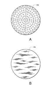
[0009] FIG. 1A is a diagram illustrating a plurality of points of light
produced by a plurality of LEDs, before an example system of the subsequent
figures is applied to a plurality of LEDs.
[0010] FIG. 1B is a diagram illustrating a plurality of points of light,
after an
example system of the subsequent figures is applied to the LEDs of FIG. 1A.
[0011] FIG. 2 is a block diagram illustrating an example system
implementing a backlighting apparatus, showing some detail of a substrate
wrapped around an edge of a lightguide, according to an implementation.
[0012] FIG. 3 is a block diagram illustrating an example system
implementing a keyboard assembly, showing some detail of a deadfront
keyboard, according to an implementation.
[0013] FIG. 4 is a block diagram illustrating an example system
implementing a backlighting apparatus, showing some detail of a substrate
that has light-generating sources disposed at a diffusive side, according to
an
implementation.
[0014] FIG. 5 is a block diagram illustrating an example system
implementing a backlighting apparatus, showing some detail of light-
generating sources configured to emit light into a lightplate, according to an
implementation.
3
CA 02949223 2016-11-15
WO 2015/176044
PCT/US2015/031254
[0015] FIG. 6 is a block diagram illustrating an example system
implementing a backlighting apparatus, showing some detail of a substrate
that has light-generating sources disposed opposite a prismatic diffusion
layer,
according to an implementation.
[0016] FIG. 7 is a block diagram illustrating an example system
implementing a backlighting apparatus, showing some detail of light-
generating sources configured to emit light into a lightplate and a prismatic
diffusion layer, according to an implementation.
[0017] The Detailed Description references the accompanying figures. In
the figures, the left-most digit(s) of a reference number identifies the
figure in
which the reference number first appears. The same numbers are used
throughout the drawings to reference like features and components.
DETAILED DESCRIPTION
[0018] Techniques and devices provide uniform illumination, especially
backlighting. Such backlighting can be used for many devices, such as displays
or keyboards. In particular, the technology disclosed herein utilizes
substrates
that have light-generating sources with new and heretofore unachievable
properties to backlight devices. A plurality of light-generating sources are
positioned at a plurality of differing angles. Combined with diffusive layers
or
diffusive properties of a lightguide the light-generating sources create a
soft,
even backlighting in a thinner embodiment than conventional techniques. In
4
CA 02949223 2016-11-15
WO 2015/176044
PCT/US2015/031254
one example embodiment, a substrate that has light-generating sources, and
is wrapped around an edge of a lightguide.
[0019] Seemingly, all electronic devices are getting smaller and smaller.
Computing devices are getting thinner and thinner. The thinness of display
devices are constrained by many factors. Often, one of the factors that limits
the thinness of such display devices are the lighting elements of the display
devices. The thinness of the conventional display devices have been pushed to
the limit of what conventional approaches can allow.
[0020] As these devices are getting thinner, often the physical size of the
light-generating sources (e.g., light-emitting diodes (LEDs) is becoming a
limiting factor in the thinness of devices. Often LEDs are used to edge-lit a
lightguide. This is done this way to avoid having the LEDs in the directly
line-of-
sight of a display (or similar device). Doing this can create harsh points of
light.
The technology described herein describes orienting light-generating sources
(such as LEDs) in a variety of manners to utilize reflective and diffusive
properties in lightguides. These novel techniques enable the devices, for
example display devices, to be thinner, and to have a soft, even backlighting.
Thus, these display devices are both thin and do not have harsh points of
light.
[0021] Implementations described herein utilize a thin and flexible
substrate on which light-generated sources (e.g., LEDs) are operatively
connected to a circuitry on the substrate. In some implementations, the
lightguide acts as the substrate. In still other implementations, the light-
CA 02949223 2016-11-15
WO 2015/176044
PCT/US2015/031254
generating sources are disposed within the lightguide. The substrate is 0.1 to
0.15 mm thick or perhaps thinner. In some implementations, the substrate has
a thickness of 0.07 to 0.2 mm (i.e., 70 to 200 microns)
[0022] To further emphasize this advantage over conventional techniques,
Fig. 1A demonstrates an example of the failing of light-generating sources
arranged in a conventional backlighting manner. As shown, the light-
generating sources generate several harsh points of light 102. These points of
light are undesirable to a user of a display device, as they distract from the
information presented by the display device.
[0023] Conversely, Fig. 18 demonstrates an example of the novel
technology described herein. Rather than the harsh points of light 102, Fig.
18
shows a soft, even backlighting 104 of the display device. Soft, even
backlighting can decrease viewing strain.
EXEMPLARY LIGHTPLATES
[0024] FIG. 2 illustrates a system 200 implementing a backlighting
apparatus, showing some detail of a substrate wrapped around an edge of a
lightguide. For example, substrate 202 is wrapped around an edge of
lightguide 204. Lightguide 204 includes diffusive side 206 and non-diffusive
side 208. Since substrate 202 is wrapped around the edge of lightguide 204,
substrate 202 covers a portion of diffusive side 206 and a portion of non-
diffusive side 208.
6
CA 02949223 2016-11-15
WO 2015/176044
PCT/US2015/031254
[0025] Substrate 202 has several layers attached thereto. Light layer 210
includes light-generating source (LGS) 212. Layers 214 and 216 include
conductive traces. Conductive traces 214 and 216 electrically link light-
generating source 212 to a power source. The power source enables light-
generating source 212 to emit light by becoming electrically charged.
[0026] In one or more implementations, the light layer 210 on the
substrate 202 has several LEDs (e.g., printable light-emitting diodes
(pLEDs)),
that emit light into the lightguide 204 at different sides (e.g.,
surfaces/sides
and edge) of the lightguide. The orientation of the LGSs relative to the
lightguide 204 (e.g., surface/side or edge) create a plurality of differing
angles
at which the light enters the lightguide. For example, light-generating source
218 is oriented perpendicular to diffusive side 206. Further, light-generating
source 220 is oriented perpendicular to non-diffusive side 208. Also, light-
generating source 212 is oriented parallel to diffusive side 206 and non-
diffusive side 208 (or perpendicular to the edge). Thus, light-generating
source
218, light-generating source 220, and light-generating source 212 are all
oriented at different angles from each other.
[0027] Herein, references to LGSs being oriented to perpendicular to a
surface/side or an edge mean that the LGSs are oriented so that the center of
the light beam emitted from a LGS is generally perpendicular to the
surface/side or edge. Generally, perpendicular includes angles that are +/-
25%
from the literal perpendicular.
7
CA 02949223 2016-11-15
WO 2015/176044
PCT/US2015/031254
[0028] The light rays generated from the light-generating sources are
generally directed into to the surface/side or edge of the lightguide
(depending upon to which one that it is directed). For example, light emitted
from the light-generating source 212 is directed towards the edge of the
lightguide. Thus, it enters the lightguide via the edge of the lightguide.
[0029] The light from the LGSs typically enters the surface/side or edge of
the lightguide at an angle perpendicular to that surface/side or edge.
However, light beam emanating from the LGSs spreads out and proceeds at
angles other than exactly perpendicular. For example, light-generating source
222 emits light into lightguide 204 at an angle that is not perpendicular to
non-diffusive side 208. Regardless, the direction of the light beam is towards
the surface/side or edge to which it is directed/oriented.
[0030] To create the diffused light, the LGSs emit light into lightguide
204,
the light is reflected in lightguide 204, and then the light is emitted from
lightguide 204 as diffused light. For example, LGS 212 emits light ray 226
into
lightguide 204. Light ray 224 reflects off non-diffusive side 208, enters
diffusive side 206, and then is emitted as diffused light 228.
[0031] Diffusive side 206 of lightguide 204 is imbued with diffusive
properties. Diffusive side 206 may, for example, contain etchings that diffuse
light that enters diffusive side 206. Etchings may be any structure or
property
that would diffuse light passing through diffusive side 206.
8
CA 02949223 2016-11-15
WO 2015/176044
PCT/US2015/031254
[0032] Non-diffusive side 208 of lightguide 204 has different properties
than diffusive side 206. For example, non-diffusive side 208 may be
reflective.
To imbue non-diffusive side 208 with reflective properties, non-diffusive side
208 may be coated with a reflective material. A portion of non-diffusive side
may not include the reflective coating. The portion of non-diffusive side may
include etchings similar to those described above regarding diffusive side
206.
[0033] The portions of lightguide 204 under edge-wrapped substrate 202
may not include diffusive and non-diffusive properties of diffusive side 206
and non-diffusive side 208. Thus, light emitted from the LGSs may enter the
lightguide unaltered. Optionally, the diffusive properties of the portion of
diffusive side 206 under edge-wrapped substrate 202 may be retained to
create more diffused light in lightguide 204. Further, the portion of non-
diffusive side 206 under edge-wrapped substrate 202 may include diffusive
properties to create more diffused light in lightguide 204.
[0034] A conventional edge-lit lightguide has several LEDs lined upon along
the edges of a lightguide. The LEDs are oriented to direct their light into
the
edge. With this conventional arrangement, the light from the edge-mounted
LEDs enters only along the edge of the lightguide. In fact, to improve the
transfer efficiency, it is common to bridge the light path between the edge-
mounted LEDs and the edge of the lightguide with lens (e.g., prisms or Fresnel
lens). Often these LEDs and light bridges are thicker than the lightguide's
themselves. Thus, the LEDs are often the limiting factor on thinness with a
9
CA 02949223 2016-11-15
WO 2015/176044
PCT/US2015/031254
conventional edge-mounted LED arrangement of a backlighting approach.
Also, with the conventional approach, the light at the very edge of the
lightguide is not yet diffused as it enters the edge of the lightguide.
[0035] Unlike a conventional edge-lit arrangement, the implementation of
the new technology described herein maximizes light-transfer efficiency. The
substrate is thin and flexible. It has LEDs are that smaller than the
thickness of
the lightguide. The substrate is directly attached (e.g., adhered, mounted,
pressed, etc.) to the edge of the lightguide and wraps around to portion of
each surface. Because of this, the LEDs pressed immediately against the
surface/edge of the lightplate. There is no need for lens or any other light
bridge.
[0036] With this new arrangement, light from the various LEDs enter into
the lightguide from its edge as well as from at least a portion of one or both
surfaces immediately adjacent to the edge. Because of this light at the edge
of
the lightguide is immediately and quickly diffused.
[0037] In some implementations, the LGS and circuitry (e.g., conductive
traces) are printed onto the thin flexible substrate using pLEDs. In other
implantations, the LGS is a tiny LED (e.g., 20-40 microns in diameter) placed
and fixed onto the substrate with conductive links connecting them to a
potential power source.
CA 02949223 2016-11-15
WO 2015/176044
PCT/US2015/031254
[0038] FIG. 3 is a block diagram illustrating system 300 implementing a
keyboard assembly, showing some detail of a deadfront keyboard. For
example, system 300 includes deadfront keyboard overlay layer 302, sensor
layer 304, light layer 306, and backer layer 308. Light layer 306 has LGSs 310
and 312. Anteroom 314 is included in sensor layer 304 and lightroom 316 is
included in light layer 306 and sensor layer 304. LGSs 310 and 312 emit light
into anteroom 314. Light passes from anteroom 314 into lightroom 316, and
then escapes through deadfront keyboard overlay layer 302 to illuminate key
pattern 318. The light that illuminates key pattern 318 is not harsh points of
light, but rather a soft, even backlighting.
[0039] The layers of the deadfront keyboard are positioned one on top of
the other. Deadfront keyboard overlay layer 302 is on top. Deadfront keyboard
overlay layer 302 includes key patterns, for example key pattern 318 that
shows the letter "A". Key pattern 318 is not visible when system 300 is turned
off. Key pattern 318 is typically not depressable. Optionally, system 300 may
provide some manner of acknowledgment to a user when a key is pressed,
such as a change in illumination of key pattern 318, for example highlighting
key pattern 318, or a sound. When LGSs 310 and 312 are enabled, key pattern
318 becomes visible.
[0040] Sensor layer 304 is located under deadfront keyboard layer 302.
Sensor layer 304 includes anteroom 314. Sensor layer 304 also includes
CA 02949223 2016-11-15
WO 2015/176044
PCT/US2015/031254
mechanisms to detect that a key, such as key pattern 318, has been pressed.
Such a mechanism may be, for example, resistance or capacitive sensing.
[0041] Anteroom 314 in sensor layer 304 is positioned above LGSs 310 and
312. Light-generating sources emit light rays 320 and 322 into anteroom 314.
Anteroom 314 may be composed of air, transparent material, translucent
material, or any other material that will enable emitted light rays 320 and
322
to pass through anteroom 314. Anteroom 314 may be surrounded by
reflective material. This reflective material may be similar to material
included
in non-diffusive side 208. Emitted light rays 320 and 322 reflect off the
sides of
anteroom 314, and exit anteroom 314 into lightroom 316.
[0042] Light layer 306 is positioned under sensor layer 304. Light layer
306
includes LGSs 310 and 312 and lightroom 316.
[0043] LGSs 310 and 312 are similar to LGSs 212, 218, 220, and 222. LGSs
310 and 312 are operatively linked to a light driver, and the light driver is
configured to drive the LGSs 310 and 312. For example, the light driver may be
a power source and the light driver may be operatively linked to LGSs 310 and
312 via structures similar to conductive traces 214 and 216.
[0044] Lightroom 316 is configured to receive emitted light rays 320 and
322 from anteroom 314. Lightroom 316 may be composed of air, transparent
material, translucent material, or any other material that will enable emitted
light rays 320 and 322 to pass through lightroom 314. Lightroom 314 may be
12
CA 02949223 2016-11-15
WO 2015/176044
PCT/US2015/031254
surrounded by reflective material. This reflective material may be similar to
material included in non-diffusive side 208. Emitted light rays 310 and 312
reflect off the sides of lightroom 316, and illuminate key pattern 318 with
diffused light 324. Emitted light rays 320 and 322 exit system 300 through
deadfront keyboard overlay layer 302. Diffused light 324 is not harsh points
of
light, but rather provides a soft, even backlighting.
[0045] Backer layer 308 is located under light layer 306. Backer layer 308
may include reflective material, similar to material included in non-diffusive
side 208. The reflective material of backer layer 308 keeps emitted light rays
320 and 322 in lightroom 316 until emitted light rays 320 and 322 exit
lightroom 316 through deadfront keyboard overlay layer 302 and illuminate
key pattern 318.
[0046] FIG. 4 illustrates a system 400 implementing a backlighting
apparatus, showing some detail circuitry with light-generating sources
disposed at a diffusive side of a lightguide. For example, circuit 402 has LGS
404 with conductive traces contained within layers 406 and 408.
[0047] Similar to the system 200, LGS 404 is oriented so that LGS 404 emits
light into lightguide 410. As depicted, conductive trace 408 is translucent or
transparent to allow light to pass therethrough. The emitted light ray 412
passes through diffusive side 414 of lightguide 410. The emitted light ray 412
reflects off non-diffusive side 416 of lightguide 410 back into lightguide 410
towards diffusive side 414. Diffusive side 414 diffuses emitted light ray 412,
13
CA 02949223 2016-11-15
WO 2015/176044
PCT/US2015/031254
resulting in diffused light 418 emitting from lightguide 410. Diffused light
418
is not harsh points of light, but rather provides a soft, even backlighting
for
system 400.
[0048] Rather than using a single-purpose substrate to print/place the
circuit thereon, the lightguide itself acts as the substrate for the circuit.
More
particularly, the circuits (e.g., 402, 420, and 422) are printed/placed on the
diffusive side 414. As depicted, the LGS 404 may contain a single LGS. Or it
may contain a plurality of such sources.
[0049] Fig. 5 is a block diagram illustrating a system 500 implementing a
backlighting apparatus, showing some detail of LGSs configured to emit light
into a lightplate, according to an implementation. For example, rather than
substrate 402 disposed at diffusive side 502, a LGS layer 504 including LGSs
506-510 and conductive layers 512 and 514 may be included in system 500.
[0050] Similar to system 200, LGS 506 is oriented so that LGS 506 emits
light into lightplate 516. The emitted light ray 518 passes through
translucent
or transparent conductive trace 514 and lightplate 516. The emitted light ray
518 reflects off non-diffusive side 520 of system 500 back into lightplate 516
towards diffusive side 502. Emitted light ray passes through lightplate 516,
conductive traces 512 and 514, and light-generating source layer 504.
Diffusive
side 502 diffuses emitted light ray 518, resulting in diffused light 522
emitting
from system 500. Diffused light 522 is not harsh points of light, but rather
provides a soft, even backlighting for system 500.
14
CA 02949223 2016-11-15
WO 2015/176044
PCT/US2015/031254
[0051] Fig. 6 is a block diagram illustrating a system 600 implementing a
backlighting apparatus, showing some detail of a circuitry including LGSs
disposed opposite a prismatic diffusion layer. For example, lightguide 602
includes a circuitry 604 similar to circuitry 402. LGS 606 of circuit 604
emits
light ray 608 into lightguide 602. Nano-resolution tools at prismatic
diffusion
layer 610 of lightguide 602 diffuse emitted light ray 608, resulting in
diffused
light 612 emitting from lightguide 602. Diffused light 612 is not harsh points
of
light, but rather provides a soft, even backlighting for system 600.
[0052] Nano-resolution tools include ultrathin lenses, embossed areas,
and other structures that would occur to one of ordinary skill in the art.
Nano-
resolution tools may diffract, refract, or diffuse emitted light ray 612.
[0053] Substrate 604 also has conductive traces 614 and 616. Conductive
traces 614 and 616 are similar to conductive traces 406 and 408.
[0054] Rather than using a single-purpose substrate to print/place the
circuit thereon, the lightguide itself acts as the substrate for the circuit.
More
particularly, the circuits (e.g., 602, 618, and 620) are printed/placed on the
non-diffusive side. As depicted, the LGS 606 may contain a single LGS or it
may
contain a plurality of such sources.
[0055] Fig. 7 is a block diagram illustrating a system 700 implementing a
backlighting apparatus, showing some detail of light-generating sources
configured to emit light into a lightplate and a prismatic diffusion layer.
For
CA 02949223 2016-11-15
WO 2015/176044
PCT/US2015/031254
example, system 700 includes a LGS layer 702 and conductive trace layers 704
and 706, similar to light-generating source layer 504 and conductive trace
layers 512 and 514. LGS 708 emits light ray 710 into lightplate 712. Emitted
light ray 710 passes through conductive trace 704, lightguide 712, and
prismatic diffusion layer 714. Nano-resolution tools at prismatic diffusion
layer
714 of system 700 diffuse emitted light ray 710, resulting in diffused light
716
emitting from system 700. Diffused light 716 is not harsh points of light, but
rather provides a soft, even backlighting for system 700. Nano-resolution
tools
of system 700 are similar to nano-resolution tools of system 600.
[0056] The exemplary systems of Figs. 2-7 may also be constructed as an
article of manufacture. An article of manufacture exhibits similar properties
to
systems 200, 300, 400, 500, 600, and 700.
LIGHT-GENERATING SOURCES
[0057] As utilized herein, the term "light-generating sources" (LGS) refers
to any device that emits electromagnetic radiation within a wavelength regime
of interest, for example, visible, infrared or ultraviolet regime, when
activated,
by applying a potential difference across the device or passing a current
through the device. Examples of LGSs include solid-state, organic, polymer,
laser diodes or other similar devices as would be readily understood. The
emitted radiation of a LGS may be visible, such as red, blue or green, or
invisible, such as infrared or ultraviolet. A LGS may produce radiation of a
16
CA 02949223 2016-11-15
WO 2015/176044
PCT/US2015/031254
spread of wavelengths. Unless the context states otherwise, a reference to a
LGS may include multiple LGSs, each emitting essentially the same or different
wavelengths. In some embodiments, a LGS is an unpackaged LED (e.g., LED
die).
[0058] To promote thinness and smallness, many implementations
contemplate the use of unpackaged LEDs (e.g., LED dies) instead of packaged
LEDs. Further, the individual LGS (e.g., unpacked LED) contemplated have a
diameter between 10 to 50 microns and a height between 5 to 20 microns. In
some implementations, the light-generating component has a diameter
between about 20 to 30 microns and a height between about 5 to 15 microns.
In some implementations, the size of the individual LGS (e.g., unpackaged LED)
is 25 to 50 microns.
[0059] An example of a LGS that is contemplated to be used with the
technology described herein is described in U.S. Patent 8,415,879, which is
titled "Diode for a Printable Composition," which is incorporated by reference
herein. These LEDs are printed, thus they are called pLEDs herein.
[0060] Each pLED has a diameter between 10 to 50 microns and a height
between 5 to 20 microns. In some implementations, the light-generating
component has a diameter between about 20 to 30 microns and a height
between about 5 to 15 microns.
17
CA 02949223 2016-11-15
WO 2015/176044
PCT/US2015/031254
[0061] Using the pLEDs, each group of LGSs may contain about two-
thousand sources in some implementations. In other implementations, a
group may contain as much as five thousand source.
[0062] Implementations of the technology described herein that use the
pLEDs involve a disposition, for example placing the pLEDs through printing or
spraying, of pLEDs that are suspended in a liquid or gel, for example ink.
Indeed, the disposition of pLEDs may be accomplished on a convention
printing press or screen press.
[0063] The structure created by disposing the pLEDs may also be called a
printed "circuit" In some implementations, the printed circuit is a thin stack
of
layers on a substrate, which is a thin film. That film is 0.1 to 0.15 mm thick
or
perhaps thinner. In some implementations, the film has a thickness of 0.07 to
0.2 mm. This film of material may be a polyester film or other suitable
material. The combined stack is only microns thicker than the film itself.
ADDITIONAL AND ALTERNATIVE IMPLEMENTATION NOTES
[0064] Any suitable type of technology can be utilized to implement
conductive traces. Examples of suitable technologies include (by way of
example and not limitation): silver, carbon-like material, or any other
material
for conducting electricity that would occur to one of ordinary skill in the
art.
The conductive traces may be composed of material that is reflective, opaque,
or otherwise not translucent nor transparent. The conductive traces may
18
CA 02949223 2016-11-15
WO 2015/176044
PCT/US2015/031254
include conductive nano-fibers. Conductive traces may be created using
conventional conductive ink or other similar processes. Conductive inks may
be classed as fired high solids systems or PTF polymer thick film systems that
allow circuits to be drawn or printed on a variety of substrate materials such
as
polyester to paper. These types of materials usually contain conductive
materials such as powdered or flaked silver and carbon like materials. While
conductive inks can be an economical way to lay down a modern conductive
traces, traditional industrial standards such as etching of conductive traces
may be used on relevant substrates
[0065] Any suitable type of technology can be utilized to implement the
etchings of diffusive side 206. Examples of suitable technologies include (by
way of example and not limitation): a material, such as phosphor, that coats
diffusive side 206, structures in diffusive side 206, or molds attached to
diffusive side 206. Structures in diffusive side 206 may include ablations,
excisions, abscissions, cuts, engravings, imprints, incisions, corrosions,
abrasions, dissolutions, erosions, oxidations, or any other structure that
would
occur to one of ordinary skill in the art. Molds attached to or integral with
diffusive side 206 may include protrusions, nodules, bumps, convexities,
ridges, bulges, or any other structure that would occur to one of ordinary
skill
in the art.
[0066] Any suitable type of technology can be utilized to implement the
mechanisms of sensor layer 304. Examples of suitable technologies include
19
CA 02949223 2016-11-15
WO 2015/176044
PCT/US2015/031254
(by way of example and not limitation): resistive, capacitive, or contact
switches, or other mechanisms that will occur to those of ordinary skill in
the
art. Sensor layer 304 may also be composed of a web or membranes of
circuitry, or other structures that will occur to those of ordinary skill in
the art.
[0067] Any suitable type of technology can be utilized to implement the
nano-resolution tools. Examples of suitable technologies include (by way of
example and not limitation): Nano-resolution tools include structures such as
linear diffusers, industrex, saute softening diffusers, frosted diffusers, or
others that will occur to those of ordinary skill in the art.
[0068] In the above description of exemplary implementations, for
purposes of explanation, specific numbers, materials configurations, and other
details are set forth in order to better explain the present invention, as
claimed. However, it will be apparent to one skilled in the art that the
claimed
invention may be practiced using different details than the exemplary ones
described herein. In other instances, well-known features are omitted or
simplified to clarify the description of the exemplary implementations.
[0069] The inventors intend the described exemplary implementations to
be primarily examples. The inventors do not intend these exemplary
implementations to limit the scope of the appended claims. Rather, the
inventors have contemplated that the claimed invention might also be
embodied and implemented in other ways, in conjunction with other present
or future technologies.
CA 02949223 2016-11-15
WO 2015/176044
PCT/US2015/031254
[0070] Moreover, the word "exemplary" is used herein to mean serving as
an example, instance, or illustration. Any aspect or design described herein
as
"exemplary" is not necessarily to be construed as preferred or advantageous
over other aspects or designs. Rather, use of the word exemplary is intended
to present concepts and techniques in a concrete fashion. The term
"techniques," for instance, may refer to one or more devices, apparatuses,
systems, methods, articles of manufacture, and/or computer-readable
instructions as indicated by the context described herein.
[0071] As used in this application, the term "or" is intended to mean an
inclusive "or" rather than an exclusive "or." That is, unless specified
otherwise
or clear from context, "X employs A or B" is intended to mean any of the
natural inclusive permutations. That is, if X employs A; X employs B; or X
employs both A and B, then "X employs A or B" is satisfied under any of the
foregoing instances. In addition, the articles "a" and "an" as used in this
application and the appended claims should generally be construed to mean
"one or more," unless specified otherwise or clear from context to be directed
to a singular form.
OTHER WAYS OF DESCRIBING IMPLEMENTATIONS
[0072] Below is a listing of different ways to describe the implementations
introduced here:
21
CA 02949223 2016-11-15
WO 2015/176044
PCT/US2015/031254
[0073] Example A; An implementation of a backlighting apparatus
comprising:
= a translucent lightguide including a diffusive side and a non-diffusive
side,
the diffusive side and the non-diffusive side disposed at opposite sides of
the lightguide;
= a substrate wrapped around an edge of the lightguide and disposed at the
lightguide at both the diffusive side and the non-diffusive side, such that
the substrate covers a portion of the diffusive side and a portion of the
non-diffusive side;
= a plurality of light-generating sources of the substrate configured to
emit
light into the lightguide through the edge and at least one side of the
I ightguide;
= a reflective coating disposed at the non-diffusive side configured to
reflect
the emitted light from the light-generating sources back into the lightguide
towards the diffusive side.
[0074] An implementation of backlighting apparatus of Example A that
further comprising etchings of the diffusive side configured to diffuse the
reflected light and emit the diffused light out of the lightguide.
[0075] An implementation of backlighting apparatus of Example A,
wherein the plurality of light-generating sources include light-emitting
22
CA 02949223 2016-11-15
WO 2015/176044
PCT/US2015/031254
semiconductors that each have a cross-section with a maximum height
between 5 to 20 microns and a diameter between 10 to 50 microns.
[0076] An implementation of backlighting apparatus of Example A,
wherein the light-generating sources include light-emitting diodes.
[0077] An implementation of backlighting apparatus of Example A,
wherein the substrate is flexible and thin, having a thickness of 70 to 200
microns.
[0078] An implementation of backlighting apparatus of Example A,
wherein the plurality of light-generating sources are oriented to cast its
light in
directions that include perpendicular to the diffusive side, perpendicular to
the non-diffusive side, and parallel to the diffusive side and the non-
diffusive
side.
[0079] An implementation of backlighting apparatus of Example A,
wherein the emitted light enters the lightguide through the diffusive side,
the
non-diffusive side, and the edge of the lightguide.
[0080] Example B: An implementation of a keyboard assembly comprising:
= a deadfront keyboard overlay layer including a key pattern that is
configured to be illuminated by a plurality of light-generating sources;
= a sensor layer configured to determine selection of a key indicated by
the
key pattern, the sensor layer being positioned under the overlay layer, the
23
CA 02949223 2016-11-15
WO 2015/176044
PCT/US2015/031254
sensor layer having an anteroom defined therein, the anteroom including
reflective material;
= a light layer that is positioned under the sensor layer, the light layer
having
one or more light-generating sources configured to emit light into the
anteroom of the sensor layer;
= the sensor layer and the light layer having a lightroom defined therein
and
positioned underneath the key pattern, the lightroom including reflective
material;
= a light driver operatively linked to the one or more of light-generating
sources and configured to drive the one or more of light-generating
sources.
[0081]
[0082] An implementation of keyboard assembly of Example B, wherein
when the light driver drives the one or more light-generating sources, the key
pattern is illuminated by diffused light that originates from the one or more
light-generating sources.
[0083] An implementation of keyboard assembly of Example B, wherein
when the light driver drives the one or more light-generating sources, the one
or more light-generating sources emit light into the anteroom, the emitted
light reflects off the reflective material of the anteroom into the lightroom,
24
CA 02949223 2016-11-15
WO 2015/176044
PCT/US2015/031254
therein the reflected light in lightroom escapes the lightroom via the key
pattern of the deadfront keyboard overlay layer.
[0084] An implementation of keyboard assembly of Example B, wherein
the anteroom and the lightroom are composed of material selected from a
group consisting of air, transparent material, and translucent material.
[0085] An implementation of keyboard assembly of Example B, wherein
the deadfront keyboard overlay layer includes an alphanumeric keyboard
composed of a plurality of key patterns.
[0086] An implementation of keyboard assembly of Example B, wherein
the key pattern is visible in response to the plurality of light-generating
sources emitting light.
[0087] An implementation of keyboard assembly of Example B, wherein
the plurality of light-generating sources include light-emitting
semiconductors
that each have a cross-section with a maximum height between 5 to 20
microns and a diameter between 10 to 50 microns.
[0088] An implementation of keyboard assembly of Example B 3, wherein
the light-generating sources include light-emitting diodes.
[0089] An implementation of keyboard assembly of Example B, wherein
light layer is composed of a flexible and thin surface lighted substrate,
having a
thickness of 70 to 200 microns.
CA 02949223 2016-11-15
WO 2015/176044
PCT/US2015/031254
[0090] Example C: An implementation of a backlighting apparatus
comprising:
= a lightplate including a diffusive side and a non-diffusive side, the
diffusive
side and the non-diffusive side disposed at opposite sides of the lightplate;
= a plurality of light-generating sources affixed to at least one side of
the
lightguide, the light-generating sources being configured to emit light into
the lightguide through the side of the lightguide to which it is affixed;
= a reflective coating disposed at the non-diffusive side configured to
reflect
the emitted light from the light-generating sources back into the lightplate
towards the diffusive side.
[0091] An implementation of a backlighting apparatus of Example C,
further comprising etchings of the diffusive side configured to diffuse the
reflected light and emit the diffused light out of the lightplate.
[0092]
[0093] An implementation of a backlighting apparatus of Example C,
wherein the plurality of light-generating sources include light-emitting
semiconductors that each have a cross-section with a height between 5 to 20
microns and a diameter between 10 to 50 microns.
[0094] An implementation of a backlighting apparatus of Example C,
wherein the plurality of light-generating sources include light-emitting
diodes.
26
CA 02949223 2016-11-15
WO 2015/176044
PCT/US2015/031254
[0095] An implementation of a backlighting apparatus of Example C,
wherein the plurality of light-generating sources are oriented to direct its
emitted light into the lightguide and in a direction that is perpendicular to
the
diffusive side.
[0096] An implementation of a backlighting apparatus of Example C,
wherein the emitted light enters the lightguide via the diffusive side.
[0097] An implementation of a backlighting apparatus of Example C,
wherein the plurality of light-generating sources are oriented to direct its
emitted light into the lightguide and in a direction that is perpendicular to
the
non-diffusive side.
[0098] An implementation of a backlighting apparatus of Example C,
wherein the emitted light enters the lightguide via the non-diffusive side.
[0099] Example D: An Implementation of a backlighting apparatus
comprising:
= a translucent lightguide including a diffusive side and a non-diffusive
side,
the diffusive side and the non-diffusive side disposed at opposite sides of
the lightguide;
= a substrate that has a plurality of light-generating sources affixed to
at least
one side of the lightguide, the light-generating sources being configured to
emit light into the lightguide through the side of the lightguide to which it
is affixed;
27
CA 02949223 2016-11-15
WO 2015/176044
PCT/US2015/031254
= a reflective coating disposed at the non-diffusive side, configured to
reflect
the emitted light from the light-generating sources back into the lightguide
towards the diffusive side.
[00100] An implementation of a backlighting apparatus of Example D
further comprising a etchings placed at a plurality of locations of the
diffusive
side, configured to diffuse the reflected light and emit the diffused light
out of
the lightguide.
[00101] An implementation of a backlighting apparatus of Example D
wherein the plurality of light-generating sources include light-emitting
semiconductors that each have a cross-section with a height between 5 to 20
microns and a diameter between 10 to 50 microns.
[00102] An implementation of a backlighting apparatus of Example D,
wherein the plurality of light-generating sources include light-emitting
diodes.
[00103] An implementation of a backlighting apparatus of Example D,
wherein the plurality of light-generating sources are oriented to direct its
emitted light in a direction that is perpendicular to the diffusive side.
[00104] An implementation of a backlighting apparatus of Example D,
wherein the emitted light enters the lightguide via the diffusive side.
[00105] An implementation of a backlighting apparatus of Example D,
wherein the plurality of light-generating sources are oriented to direct its
emitted light in a direction that is perpendicular to the non-diffusive side.
28
CA 02949223 2016-11-15
WO 2015/176044
PCT/US2015/031254
[00106] An implementation of a backlighting apparatus of Example D,
wherein the emitted light enters the lightguide via the non-diffusive side.
[00107] Example E: An Implementation of a backlighting apparatus
comprising:
= a lightguide including a prismatic diffusion layer;
= a plurality of light-generating sources configured to emit light into the
I ightguide;
= nano-resolution tools placed at a plurality of locations of the prismatic
diffusion layer configured to diffuse the emitted light and pass the emitted
light through the prismatic diffusion layer.
[00108] An implementation of a backlighting apparatus of Example E,
wherein the nano-resolution tools are selected from a group consisting of
lenses and embossed areas.
[00109] An implementation of a backlighting apparatus of Example E,
wherein the prismatic diffusion layer is configured to perform operations on
the emitted light selected from a group consisting of diffraction, refraction,
and diffusion.
[00110] An implementation of a backlighting apparatus of Example E,
wherein the prismatic diffusion layer includes structures selected from a
group
consisting of linear diffusers, industrex, solite softening diffusers, and
frosted
diffusers.
29
CA 02949223 2016-11-15
WO 2015/176044
PCT/US2015/031254
[00111] An implementation of a backlighting apparatus of Example E,
wherein the plurality of light-generating sources include light-emitting
semiconductors that each have a cross-section with a maximum height
between 5 to 20 microns and a diameter between 10 to 50 microns.
[00112] An implementation of a backlighting apparatus of Example E,
wherein the light-generating sources include light-emitting diodes.
[00113] An implementation of a backlighting apparatus of Example E,
wherein the plurality of light-generating sources are oriented perpendicular
to
the prismatic diffusion layer.
[00114] An implementation of a backlighting apparatus of Example E,
wherein the emitted light enters the lightguide via the prismatic diffusion
layer.
[00115] Example F: An Implementation of a backlighting apparatus
comprising:
= a lightguide including a prismatic diffusion layer;
= a substrate has a plurality of light-generating sources disposed at a
side of
the lightguide opposite the prismatic diffusion layer and configured to emit
light into the lightguide;
= nano-resolution tools placed at a plurality of locations of the prismatic
diffusion layer configured to diffuse the emitted light and pass the emitted
light through the prismatic diffusion layer.
CA 02949223 2016-11-15
WO 2015/176044
PCT/US2015/031254
[00116] An implementation of a backlighting apparatus of Example F,
wherein the nano-resolution tools are selected from a group consisting of
lenses and embossed areas.
[00117] An implementation of a backlighting apparatus of Example F,
wherein the prismatic diffusion layer is configured to perform operations on
the emitted light selected from a group consisting of diffraction, refraction,
and diffusion.
[00118] An implementation of a backlighting apparatus of Example F,
wherein the prismatic diffusion layer includes structures selected from a
group
consisting of linear diffusers, industrex, solite softening diffusers, and
frosted
diffusers.
[00119] An implementation of a backlighting apparatus of Example F,
wherein the plurality of light-generating sources include light-emitting
semiconductors that each have a cross-section with a maximum height
between 5 to 20 microns and a diameter between 10 to 50 microns.
[00120] An implementation of a backlighting apparatus of Example F,
wherein the light-generating sources include light-emitting diodes.
[00121] An implementation of a backlighting apparatus of Example F,
wherein the plurality of light-generating sources are oriented perpendicular
to
the prismatic diffusion layer.
31
CA 02949223 2016-11-15
WO 2015/176044
PCT/US2015/031254
[00122] An implementation of a backlighting apparatus of Example F,
wherein the emitted light enters the lightguide via the prismatic diffusion
layer.
[00123] Example G: An Implementation of a backlighting apparatus
comprising:
= means for disposing a diffusive side and a non-diffusive side at opposite
sides;
= means for covering a portion of the diffusive side, a portion of the non-
diffusive side, and an edge of the disposing means;
= means for emitting light into the lightguide through the edge and at
least
one of the sides;
= means for reflecting the emitted light from the light-generating sources
back into the lightguide towards the diffusive side;
= means for diffusing the reflected light and emitting the diffused light
out of
the lightguide.
[00124] An implementation of a backlighting apparatus of Example G,
further comprising means for orienting the emitting means in a direction
selected from a group consisting of perpendicular to the diffusive side,
perpendicular to the non-diffusive side, and parallel to the diffusive side
and
the non-diffusive side.
32
CA 02949223 2016-11-15
WO 2015/176044
PCT/US2015/031254
[00125] An implementation of a backlighting apparatus of Example G,
wherein the diffusing means are selected from a group consisting of material
that coats the diffusive side, etchings in the diffusive side, and molds of
the
diffusive side.
[00126] Example H: An Implementation of a backlighting apparatus
comprising:
= a lightplate including a diffusive side and a non-diffusive side, the
diffusive
side and the non-diffusive side disposed at opposite sides of the lightplate;
= a plurality of light-generating sources located inside the lightplate and
between the diffusive and non-diffusive sides, the plurality of light-
generating sources being configured to emit light in a direction towards the
non-diffusive side;
= a reflective coating disposed at the non-diffusive side configured to
reflect
the emitted light from the light-generating sources back into the lightplate
towards the diffusive side.
[00127] An implementation of a backlighting apparatus of Example H,
further comprising etchings of the diffusive side configured to diffuse the
reflected light and emit the diffused light out of the lightplate.
[00128] An implementation of a backlighting apparatus of Example H,
wherein the plurality of light-generating sources include light-emitting
33
CA 02949223 2016-11-15
WO 2015/176044
PCT/US2015/031254
semiconductors that each have a cross-section with a height between 5 to 20
microns and a diameter between 10 to 50 microns.
[00129] An implementation of a backlighting apparatus of Example H,
wherein the plurality of light-generating sources include light-emitting
diodes.
34