Note: Descriptions are shown in the official language in which they were submitted.
CA 02949658 2016-11-18
WO 2015/179285
PCT/US2015/031359
SENSORED ELECTRICAL JUMPER
TECHNICAL FIELD
[0001] The invention relates to a sensored electrical jumper for medium and
high voltage
applications.
BACKGROUND
[0002] As electrical power distribution becomes more complex through the
advent of
renewable energy, distributed generation and the adoption of electric
vehicles, intelligent
electrical distribution and associated electrical sensing is becoming more
useful and even
necessary. Useful sensing may include, for example, voltage, current, and the
time
relationship between voltage and current at various locations within a power
distribution
network.
[0003] In implementing grid automation for the electrical grid, space
constraints provide a
challenge in implementing sensored devices for below grade and above grade
locations.
SUMMARY
[0004] In general, this disclosure is directed to electrical jumpers for power
cables and
other medium and high voltage applications. In particular, sensored electrical
jumpers
described herein can be used in many electrical grid applications including
replacing
existing jumpers in underground, indoor, or outdoor applications, such as at
switch
locations, capacitor bank applications, metering cabinet applications, motors,
switchgear,
and overhead terminal/riser pole applications, replacing a terminal connection
in an
existing cable installation as well as terminal connections suitable for an
initial
installation, and for inserting between two splices for manholes and direct
bury
applications.
[0005] In one aspect, a sensored electrical jumper comprises a conductor
having a first
end and a second end, the first end including a first connection interface and
the second
1
CA 02949658 2016-11-18
WO 2015/179285
PCT/US2015/031359
end including a second connection interface, a sensor section including at
least one sensor
disposed over the conductor between the first and second ends, the sensor
section sensing
at least one of current, temperature and voltage of the conductor, and a
sensor output
conduit extending from the sensor and oriented substantially perpendicular to
the
conductor axis to protect at least one sensor output wire from leakage current
or other
potential electrical damage.
[0006] The above summary of the present invention is not intended to describe
each
illustrated embodiment or every implementation of the present invention. The
details of
one or more examples of this disclosure are set forth in the accompanying
drawings and
the description below. Other features, objects, and advantages of the
disclosed techniques
will be apparent from the description and drawings, and from the claims.
BRIEF DESCRIPTION OF DRAWINGS
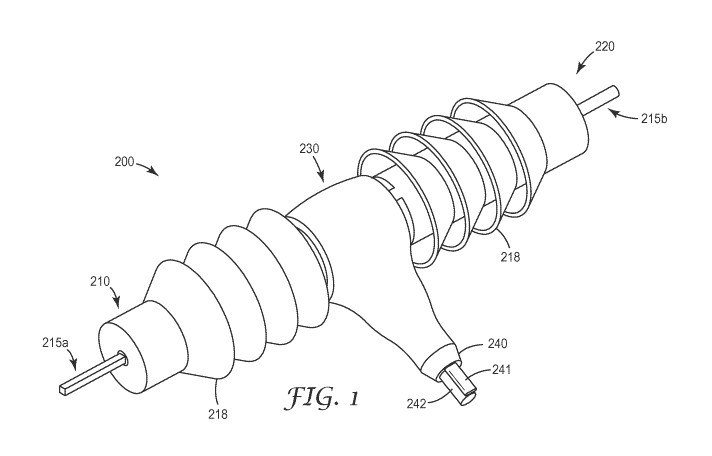
[0007] FIG. 1 is an isometric view of a sensored electrical jumper according
to an aspect
of the present invention.
[0008] FIG. 2 is a schematic view of a sensored electrical jumper showing a
partial cut
away view of the sensor section according to another aspect of the invention.
[0009] FIG. 3 is a partial cut away view of another sensored electrical jumper
showing a
partial cut away view of the sensor section according to another aspect of the
invention.
[0010] FIGS. 4A-4D show alternative implementations of the sensored electrical
jumper
according to alternative aspects of the present invention.
DETAILED DESCRIPTION
[0011] In the following Detailed Description, reference is made to the
accompanying
drawings, which form a part hereof, and in which is shown by way of
illustration specific
embodiments in which the invention may be practiced. In this regard,
directional
terminology, such as "top," "bottom," "front," "back," "leading," "forward,"
"trailing,"
etc., is used with reference to the orientation of the Figure(s) being
described. Because
2
CA 02949658 2016-11-18
WO 2015/179285
PCT/US2015/031359
components of embodiments of the present invention can be positioned in a
number of
different orientations, the directional terminology is used for purposes of
illustration and is
in no way limiting. It is to be understood that other embodiments may be
utilized and
structural or logical changes may be made without departing from the scope of
the present
invention. The following detailed description, therefore, is not to be taken
in a limiting
sense, and the scope of the present invention is defined by the appended
claims.
[0012] The present disclosure describes a sensored electrical jumper for use
in medium or
high voltage power connection applications. The sensored electrical jumper
utilizes
integrated sensor technology. The jumper configurations described herein
provide a
compact mechanism for providing real time, high accuracy voltage and/or
current
characteristics of a power cable or location in an electrical grid. The
device's compact
design allows it to fit into confined spaces and to be retrofitted into
existing systems. The
sensored electrical jumper is designed to be used in underground, indoor, or
outdoor
applications, such as at switch locations, capacitor bank applications,
metering cabinet
applications, motors, switchgear, and overhead terminal/riser pole
applications, where
reclosers, sectionalizers, capacitor banks, and primary metering are used. The
sensored
electrical jumper is particularly useful in distributed energy generation
systems, in which
devices can be geographically separated from each other. The sensored
electrical jumpers
can thus provide a utility, solar farm, wind farm, ship, industrial plant, or
any individual or
company that uses medium or high voltage equipment with the ability to create
a smart
node at many different grid locations.
[0013] In a first aspect of the invention, a sensored electrical jumper 200 is
shown in Fig.
1. The sensored electrical jumper 200 includes a conductor (see e.g., cable 12
shown in
Fig. 2 and conductor 1 shown in Fig. 3) having a first end and a second end.
In alternative
aspects, the conductor can be constructed as a solid piece of metal or a
coaxial cable, such
as a conventional medium or high voltage cable. The first end of the conductor
includes a
first connection interface 210 and the second end of the conductor includes a
second
connection interface 220. Each connection interface can be configured as, for
example, a
stem connector (such as shown in Fig. 1), a lug (such as shown in Fig. 2), a
separable
3
CA 02949658 2016-11-18
WO 2015/179285
PCT/US2015/031359
connector, a splice, a branch splice including any number of branches, and/or
a modular
connector. In an alternative aspect, a sensored jumper can include a first
conductor end
comprising a first type of connection interface and a second conductor end
comprising a
second, different type of connection interface, depending on the application
(e.g.,
connection interface 210 can comprise a stem connector, and connection
interface 220 can
comprise a lug). In another aspect of the invention, each connection interface
can
comprise one or more separable connectors or a modular connector with two or
more ends.
[0014] A sensor section 230 includes a sensor disposed over the conductor
between the
first and second ends. As shown in the examples of Figs. 2 and 3, the sensor
can be
configured to sense at least one of current, temperature and voltage.
Different sensor
constructions are provided in more detail below. In addition, the sensored
electrical
jumper 200 further includes a sensor output conduit 240 that extends from the
sensor and
is oriented substantially perpendicular to the conductor axis to protect at
least one sensor
output wire, such as output wire 242, from leakage current and other potential
electrical
damage. In addition, a jumper ground wire 241 can also be routed through
sensor output
conduit 240 to maintain ground potential. The jumper ground wire 241 will
carry the fault
current in case there is a flashover or fault so that the fuse or breaker
feeding the sensored
jumper will trip and eliminate the flow of current. In some aspects, sensor
output conduit
240 can comprise a flexible conductive or nonconductive conduit.
[0015] As also shown in Fig. 1, the sensored electrical jumper 200 can include
dielectric
stress control features to mitigate the potential for leakage current and
electrical failure.
For example, the stress control features can be implemented as multiple skirts
218
protruding outward which serve to reduce leakage currents from the exposed
stem
connectors 215a and 215b. As mentioned above, the sensored electrical jumper
can be
used in underground, indoor, or outdoor applications, such as at switch
locations, capacitor
bank applications, metering cabinet applications, and overhead terminal/riser
pole
applications, where reclosers, sectionalizers, capacitor banks, and primary
metering are
used.
4
CA 02949658 2016-11-18
WO 2015/179285
PCT/US2015/031359
[0016] Figs. 2 and 3 provide alternative configurations for the sensor
construction utilized
in the sensored electrical jumper. As would be apparent to one of skill in the
art given the
present description, other sensor configurations may also be implemented.
[0017] Fig. 2 is an alternate embodiment showing sensored electrical jumper
300. The
sensored electrical jumper 300 includes a conductor that is configured as
cable 12. Cable
12 includes an inner conductor 14, an insulation layer 16 surrounding inner
conductor 14,
and a conductive or semiconductor layer (hereinafter referred to as
semiconductor layer)
18 surrounding insulation layer 16. In other aspects, additional layers of the
cable 12,
such as a metallic cable screen surrounding semiconductor layer 18 and an
outer cable
jacket surrounding the metallic cable screen may be removed. However, in some
embodiments, these layers may remain on a portion of cable 12. The first end
of the inner
conductor 14 includes a first connection interface 310 and the second end of
the inner
conductor 14 includes a second connection interface 320. In this aspect, each
connection
interface can be configured as a lug 34.
[0018] In this embodiment, voltage and current sensors are integrated in
sensor section
330. In the illustration of Fig. 2, insulating layer 16, semiconductive layer
18 of cable 12,
as well as the sensors and some related elements are not shown in cross
section. In
addition, as shown in Fig. 2, a stress control tube 36, tubular sleeve 52, and
insulating
layer 107 are shown in cross section. In this aspect, stress control tube 36
comprising an
inner High K layer 38 and an outer insulation layer 40 is mounted on the end
portion of
cable 12 adjacent lug 34 and extends along the sensored electrical jumper 300
such that it
overlaps at least a portion of semiconductive layer 18 of cable 12. Stress
control tube 36
can be made of a shrinkable material, such as silicone or EPDM. It may be heat
or cold
shrinkable material. In the embodiment of Fig. 2, sensored electrical jumper
300 further
comprises a tubular sleeve 52 that extends over at least a portion of the
conductor ends and
the sensor section 330. Tubular sleeve 52 comprises an insulating layer of a
shrinkable
material, typically silicone or EPDM. It may be heat or cold shrinkable
material.
Alternatively, the sleeve 52 may be an overmolded or push-on layer.
Optionally, in the
illustrated embodiment, tubular sleeve 52 includes skirts 56 near the end
portions of the
5
CA 02949658 2016-11-18
WO 2015/179285
PCT/US2015/031359
jumper 300. The skirts serve to reduce leakage current, which is particularly
useful for
outdoor applications.
[0019] As shown in Fig. 2, annular strips of semiconductive layer 18 are
removed to form
non-conductive axial sections or gaps 100 in the semiconductor layer at which
gaps the
underlying insulation layer 16 is exposed. The portions of semiconductive
layer 18
separated by gaps 100 are labeled 18a, 18b, and 18c for clarity. In an
alternate
embodiment, semiconductive layer 18 may terminate with portion 18a and pieces
of a
conductive or semiconductive material may be positioned on cable 12 to serve
the same
functions as portions 18b and 18c of semiconductive layer 18. In another
alternate
embodiment, a conductive or semiconductive material attached to the back of
voltage
sensor 102, prior to its attachment to interface cable 12, may be used in
place of portion
18b of semiconductive layer 18. In yet another embodiment, voltage sensor 102
is
attached directly to the insulation layer of cable 12.
[0020] As illustrated in Fig. 2, a voltage sensor 102 is placed on
semiconductive layer
portion 18b, which is electrically isolated from portions 18a and 18c by gaps
100.
Although the present specification refers to attaching a sensor to cable 12,
in some
embodiments, the cable 12 itself functions as part of the sensor. In such
instances, the
reference herein to voltage sensor 102 refers to the portion of the sensor,
e.g., a printed
circuit board (PCB, not shown), which is attached to cable 12. In at least one
embodiment
of the present invention, the voltage sensor is a capacitive divider in which
a first capacitor
includes the cable inner conductor 14, the cable insulation layer 16, and
semiconductive
portion 18b. The second capacitor(s) are placed on a PCB, which is attached to
semiconductive layer portion 18b. The inner electrical resistance of the
semiconductive
layer portion 18b is not significant.
[0021] In some examples, the PCB may be adapted to support a plurality of
electronic
components, which may serve other purposes, e.g. safety mechanisms for in case
of
ground fault and components that form electronic circuits for temperature
compensation or
additional sensing such as temperature, humidity, magnetic field, etc.
6
CA 02949658 2016-11-18
WO 2015/179285
PCT/US2015/031359
[0022] Strips of insulating material (not shown) cover gaps 100 to separate
semiconductive portion 18b from any other conductive or semiconductive
material or
elements, except from the voltage sensor 102, and to prevent the presence of
air in gaps
100, which air could cause a partial electrical discharge and a failure of
voltage sensor
102. The insulating material may be any suitable material such as a
combination of mastic,
which will more easily fill gaps 100, and PVC tape placed over the mastic. The
PVC tape
may also serve the purpose of attaching the voltage sensor 102 to cable 12.
Voltage sensor
102 measures the voltage of the inner conductor 14 of cable 12.
[0023] A ground plate of voltage sensor 102 is electrically connected (via
e.g., grounding
wire 341 which is connected to conductive element 104a) to one or both of
semiconductive layer portions 18a and 18c by a conductive element 104.
Conductive
elements 104, 104a may comprise wire mesh that can be wrapped around one or
both of
semiconductive layer portions 18a and 18c. Conductive elements 104 can be
soldered to a
connection point 106 on voltage sensor 102. If the portion of conductive
element 104
bridging from semiconductive layer portions 18a and 18c to the voltage sensor
102 are not
insulated, the strips of insulating material (not shown) over gaps 100 will
prevent it from
making electrical contact with the underlying semiconductive portion 18b.
[0024] Insulation layer 107 covers voltage sensor 102 and the portions of
semiconductive
layer adjacent gaps 100. A layer of conductive or semiconductor material (not
shown) is
placed over insulation layer 107. In at least one embodiment, the layer of
conductive or
semiconductive material is combined with insulative layer 107 so that
insulative layer 107
has an insulative layer facing the sensor and a layer of conductive or
semiconductive
material facing stress control tube 36. The conductive or semiconductive layer
shields the
sensor from external electrical fields. Stress control tube 36 covers
insulation layer 107
and extends to the ends of cable 12 to which lugs 34 are attached. A current
sensor 108
can also be included and can be positioned over semiconductive layer 18
adjacent to
voltage sensor 102. Signal wire 110 is connected to voltage sensor 102 and
signal wire
112 is connected to current sensor 108, which may be a Rogowski coil. Both
wires 110,
112 are insulated so as not to cause any shorting. The voltage signal wire 110
and the
7
CA 02949658 2016-11-18
WO 2015/179285
PCT/US2015/031359
current signal wire 112 exit the sensor section 330 of the sensored electrical
jumper 300
via a sensor output conduit 340 (constructed in a manner similar to that
described above)
that extends from the sensor and is oriented substantially perpendicular to
the conductor
axis (e.g., the axis of inner conductor 14) to protect the sensor output
wire(s), from leakage
current and other potential electrical damage. In this aspect, ground wire 341
can exit
separately from sensor output conduit 340. In addition, current collectors
319, such as
metal straps, can be wrapped around sleeve 52 and connected to ground via
ground wire
341 to collect leakage current and provide additional protection against
flashover.
[0025] Both signal wires 110, 112 pass to the outside of sensored electrical
jumper 300
where they may be connected to, for example, a remote terminal unit that
processes
current and or voltage data from the sensor section, or an integrator, a
measuring device, a
control device, or other suitable types of devices.
[0026] In at least one embodiment, voltage sensor 102 comprises a double sided
flexible
printed circuit board. In this aspect, the top or front of the PCB is the
portion that faces
insulative layer 107. The top of the PCB typically includes conductive
features that are
electrically connected to external devices. The bottom or back of the PCB
faces cable 12.
To establish the suitable electrical contact between sensor 102 and
semiconductive layer
portion 18b, it is desirable to maximize the contact area on the back of
sensor 102. In
alternative aspects, a copper foil or gold-plated copper foil can be utilized.
[0027] In other aspects, a patterned gold-plated copper layer can be utilized.
The pattern
may be formed in any suitable manner. For example, a photoresist process may
be used to
create the pattern by applying and developing a photoresist layer on the
bottom copper
layer of the circuit board (and optionally on portions of the top copper layer
outside of the
portion circuitized for the sensor to function) in a pattern that exposes
areas of the copper
layer to be removed to create the desired copper pattern. The exposed portions
of the
copper layer(s) may then be exposed to a copper etchant solution to remove the
exposed
areas of copper. The patterned photoresist is then removed, leaving a pattern
of copper on
the bottom side of the circuit board. A layer of nickel is then plated on the
copper and
gold or a gold alloy (sometimes referred hereinafter only as gold) is then
plated on the
8
CA 02949658 2016-11-18
WO 2015/179285
PCT/US2015/031359
nickel layer. The patterned gold-plated copper layer of the PCB ensures a good
electrical
connection between semiconductive layer portion 18b and the conductive vias of
the PCB
that connect to the electrical circuit elements on the top surface of the PCB.
In one aspect,
the output signals from the voltage sensor are low voltage. For example, the
output
signals from the voltage sensor can be on the order of about 1-10 Volts with a
current on
the order of microamperes.
[0028] Like a solid layer, a patterned gold-plated copper layer of this aspect
of the present
invention will provide a nearly infinite amount of contact points. The
distance from one
contact point to another is insignificant, as it is with a solid layer. The
pattern created in
the copper layer may be any suitable pattern, including but not limited to, a
grid with a
square or diamond shaped pattern. In addition, the voltage sensor PCB of this
aspect can
differ from standard PCBs in that standard PCBs have solder resist layers
covering the
front and back surfaces of the PCB, except for conductive areas at which
electrical contact
(typically by soldering) will be made.
[0029] In addition to the foregoing, mechanical stress applied to the PCB can
be limited.
The PCB is subject to mechanical stress when it is bent and placed around
cable 12.
Although this bent configuration may place some stress on the PCB, once it is
affixed to
cable 12, e.g., with a PVC tape, and especially after stress control tube 36
and tubular
sleeve 52 are shrunk down around the interface cable 12, thereby applying a
radial force to
the PCB of voltage sensor 102, the flexible PCB remains in a relatively static
state.
Alternatively, stress control tube 36/sleeve 52 can be overmolded or pushed on
to the
jumper.
[0030] Fig. 3 is a schematic, partial cut-out view of a longitudinal section
of a sensored
electrical jumper 100, with the connection interface portions not shown, and
the sensor
section 130 shown in detail. The connection interface portions can be the same
as
described above. The sensor section 130 is disposed over a conductor 1, which
can be a
solid metal conductor, a bus bar, or a conventional power cable conductor.
[0031] The sensor 30 in this aspect is a combined voltage and current sensor.
In this
manner, space savings can be accomplished as the current sensor can be
radially
9
CA 02949658 2016-11-18
WO 2015/179285
PCT/US2015/031359
concentric with the voltage sensor. This configuration conserves space
longitudally,
allowing jumper 100 to be shorter in length, which may be advantageous for
some
applications such as capacitor banks and metering cabinets. In addition, in
this aspect of
the invention, the voltage sensor can be formed using a temperature stable
material.
[0032] The voltage sensor portion 29 has a tubular shape surrounding conductor
1. A
tubular-shaped voltage sensing device may have a shape of a hollow cylinder.
It may have
the shape of a ring or a short tube. The voltage sensor portion 29 may have
the shape of a
bent or distorted tube. The voltage sensing device may have the shape of a
rectangular
tube, i.e. in a cross section, its outer profile may have the shape of a
rectangle. The
passageway may, for example, have a circular cross section, an elliptical or
an oval cross
section, or a rectangular or triangular or any angular or irregular cross
section. In a specific
embodiment, the outer shape of the voltage sensing device has the shape of a
cylinder, and
the passageway has a circular cross section and extends through the cylinder
along the
symmetry axis of the cylinder. The voltage sensor can have a construction
similar to that
described in EP Application No. EP 13198139.1, filed December 18, 2013,
incorporated
by reference herein in its entirety.
[0033] The voltage sensor 29 includes an inner electrode or shield layer 2 in
contact with
conductor 1. The inner electrode 2 is disposed on a carrier element 3. The
carrier element
3 comprises a radially-inner (or inner) surface on which the inner electrode 2
is arranged,
and a radially-outer (or outer) surface on which an outer electrode or outer
shield layer 4 is
arranged. In this aspect, the carrier element 3 is solid, electrically non-
conductive and
comprises a material which has a coefficient of thermal expansion of less than
5x 10' 1/K
at 20 C. The carrier element 3 may, for example, comprise a ceramic material.
Many
ceramic materials have a coefficient of thermal expansion of less than 5x 10'
1/K at 20 C.
A low coefficient of thermal expansion may provide for an almost constant
radial distance
between the inner electrode and the outer electrode, when the temperature of
the carrier
element varies. This, in turn, may result in a lower variability with
temperature of the
capacitance of the sensing capacitor formed by the inner electrode, the outer
electrode and
the first portion of the carrier element. The overall accuracy of the voltage
sensor is
CA 02949658 2016-11-18
WO 2015/179285
PCT/US2015/031359
thereby improved, and/or the requirements to compensate for variations of the
sensor
output with temperature are relieved or even obsolete. Generally, a ceramic
material
further offers advantages in mechanical stability and electrical insulation
properties.
[0034] In this aspect, the ceramic material can comprise silicon nitride
(Si3N4). The
coefficient of thermal expansion of this ceramic material is approximately 2.5
x 10' 1/K at
a temperature of 20 C. When the voltage sensing device 29 and the carrier
element 3 heat
up, the carrier element 3 expands only by a very small amount, which results
in the
electrodes 2, 4 having almost the same radial distance, within a wide
temperature range.
[0035] A plurality of lamellae (not shown) provide electrical contact between
the
conductor 1 and the inner electrode 2. A plurality of lamellae or ridges can
provide for
more contact points and thus for a better electrical connection. Also, a
plurality of lamellae
provide for a certain degree of redundancy, so that the contact between
conductor 1 and
inner electrode 2 is still present, even if one lamella breaks or fails.
[0036] The inner electrode 2 may comprise an electrically conductive metal,
such as
copper, silver, gold, nickel, aluminum, or an alloy comprising any of these
materials. The
inner electrode may comprise an electrically conductive polymer. Independent
of other
features, the radial thickness of the inner electrode may be between 1
micrometer and 1
millimeter. The inner electrode may comprise a non-ferromagnetic material,
such as to
transmit an electromagnetic field generated by the power-carrying conductor 1.
It may, for
example, comprise nickel-phosphor or an alloy comprising nickel-phosphor.
[0037] The outer electrode 4 of the voltage sensor 29 can comprises a nickel-
phosphor
plating, arranged on the outer surface of the carrier element 3. Nickel-
phosphor provides a
sufficient hardness and does not corrode quickly. It also facilitates
soldering, so that a wire
can be connected to the outer electrode 30 easily. An additional layer of gold
may be
provided for even better electrical conductivity. Generally, the outer
electrode may
comprise any suitable conductive material, such as copper, silver, or gold. In
the conductor
axial direction, the outer electrode 4 extends up to an outer electrode edge
such that the
path between the inner electrode edge and the outer electrode edge along the
surface of the
carrier element 3 has a length sufficient to considerably reduce the risk of
surface
11
CA 02949658 2016-11-18
WO 2015/179285
PCT/US2015/031359
breakdown between the electrodes 2, 4, when the voltage difference between the
electrodes is in the medium- or high-voltage range, i.e. between 1 kilovolt
and 110
kilovolts. In alternative aspects, the profile of the outer electrode 4 can be
a straight line,
i.e. all portions of the outer electrode 4 are radially equally close to the
conductor axis, or
the outer electrode 4 can have a curved profile with respect to the conductor
axis.
[0038] The inner electrode 2 and the outer electrode 4 can be operated as two
electrodes of
a sensing capacitor. A middle portion of the carrier element 3 is arranged
between the
inner electrode 2 and the outer electrode 4. This middle portion can be
operated as a
dielectric of this sensing capacitor. The sensing capacitor can be connected
in series with a
secondary capacitor (PCB 5), similar to the PCB described above with respect
to Fig. 2, so
that the sensing capacitor and the secondary capacitor form a capacitive
voltage divider.
The capacitive voltage divider can then be used to sense the voltage of the
inner conductor
1.
[0039] A printed circuit board (PCB) 5 is disposed on the outer electrode 4 of
the voltage
sensor 29. PCB 5 can comprise a double sided flexible printed circuit board.
In this
aspect, the top or front of the PCB 5 faces an insulation layer 6, radially
disposed over
PCB 5. The top of the PCB typically includes conductive features that are
electrically
connected to external devices via output signal wire 41. The bottom or back of
the PCB 5
is disposed on outer electrode 4. To establish suitable electrical contact, it
is desirable to
maximize the contact area on the back of PCB 5. In alternative aspects, a
copper foil or
gold-plated copper foil can be utilized. In other aspects, a patterned gold-
plated copper
layer can be utilized.
[0040] Insulation layer 6 can comprise a conventional insulating material. The
insulating
material may be any suitable material such a combination of mastic, which will
more
easily fill gaps, and PVC tape placed over the mastic. The PVC tape may also
serve the
purpose of attaching the securing the PCB 5 to the outer electrode/carrier
element.
[0041] Optionally, a further shielding layer 7 can be arranged concentrically
around and
disposed over the insulation layer 6. Shielding layer 7 can comprise a
conventional
conductive or semiconductive material and can be used to shield the insulation
layer 6 and
12
CA 02949658 2016-11-18
WO 2015/179285
PCT/US2015/031359
the body of carrier 3. As shown in Fig. 3, shielding layer 7 can extend
axially along the
axis of conductor 1 to surround a portion of insulation layer 11, which
surrounds inner
conductor 1 outside of the sensor section 30.
[0042] As mentioned above, the sensor 30 in this aspect comprises a combined
voltage
and current sensor. As shown in Fig. 3, a current sensor 10 surrounds the
voltage sensor
29. This configuration conserves space along the axis of the conductor,
allowing jumper
100 to be shorter in length for some applications. Current sensor 10 can be
constructed
similar to sensor 108 described above.
[0043] In this aspect, the current sensor 10 can be constructed as a Rogowski
coil. The
Rogowski coil can be used to sense a current through conductor 1. The Rogowski
coil can
be flexible and can be bent to conform circumferentially around the voltage
sensor 29. The
conductive turns of the actual coil are accommodated in a non-conductive
envelope, which
electrically isolates them from the outer electrode voltage sensor 29. The
envelope can be
preferably made of a flexible polymeric material. The carrier element 3 can
include a
recess that allows it to accommodate a current sensing device 10 without
adding much to
the outer diameter of the voltage sensing device 29. This allows the voltage
sensing device
29 to be small in size.
[0044] The Rogowski coil detects the magnetic field generated by a current
through the
conductor 1 in the sensor section 130. Advantageously, the shielding layers
can comprise
electrically conductive, non-ferromagnetic material. Such material allows
magnetic fields
to be transmitted therethrough to the Rogowski coil. For example, the
shielding layers,
including the outer electrode, can comprise nickel-phosphor plating, which is
non-
ferromagnetic.
[0045] Output signals from the current sensor can be carried by current output
signal wire
42.
[0046] As shown in Fig. 3, the sensored electrical jumper 100 can include a
sensor output
conduit 340 that extends from the sensor section through anti-tracking
insulation layer 352
and is oriented substantially perpendicular to the conductor axis to protect
the sensor
13
CA 02949658 2016-11-18
WO 2015/179285
PCT/US2015/031359
output wires 41, 42 from leakage current and electrical damage. Sensor output
conduit
340 can be constructed in a similar manner as described above.
[0047] In this aspect, a jumper ground wire 45 exits the sensor section 130
outside of
sensor output conduit 340.
[0048] The sensored electrical jumper 100 further includes an insulation layer
11
surrounding the conductor 1 outside the sensor portion 130. The sensored
electrical
jumper 100 can further include a stress control layer 13 formed by a High K
material. In
one aspect, this stress control layer can be shaped as a tube that comprises
in its mounted
state an inner layer which is a stress control element and an outer dielectric
layer 15 of e.g.
silicone or ethylene propylene diene monomer rubber (EPDM). The stress control
element
may achieve stress control by the use of particular materials, such as High K
materials or
by the use of geometric stress control shapes. The stress control tube may be
fabricated by
a molding process or an extrusion process.
[0049] The sensored electrical jumper 100 further includes a tubular sleeve
352 that
extends over at least a portion of the conductor ends and the sensor section
130. Tubular
sleeve 352 comprises an anti-tracking insulation material that may be a heat
or cold
shrinkable material, an overmolded material or a push-on material. Optionally,
tubular
sleeve 352 may further include skirts near the end portions of the jumper 100.
The skirts
serve to reduce tracking current, which is particularly useful for outdoor
applications.
[0050] In addition, current collectors 19, such as metal straps, can be
wrapped around
sleeve 16 and connected to ground via ground wire 45 to collect leakage
current and
provide additional protection against flashover. Optionally, for high voltage
applications,
deflectors 22, such as geometric stress cones formed in the outer sleeve 16,
can also be
implemented.
[0051] Because the sensored electrical jumpers described herein can include a
current
sensor and a capacitive voltage sensor, these devices facilitate calculation
of phase angle
(power factor), Volt Amps (VA), Volt Amps reactive (VAr), and Watts (W).
[0052] The sensored electrical jumper can be compact in size. For example,
sensored
electrical jumpers 100, 200, 300 can have an axial length of 25 inches or
less.
14
CA 02949658 2016-11-18
WO 2015/179285
PCT/US2015/031359
[0053] The sensored electrical jumpers described herein can be utilized in a
variety of
applications. For example, for underground applications, such as in capacitor
banks or in
pad mounted, primary metering cabinets, which can include multiple current and
potential
transformers, a corresponding number of sensored electrical jumpers such as
described
herein can be utilized to enable cabinet manufacturers to decrease cabinet
size and
establish smart nodes for grid automation. For overhead applications, the
sensored
electrical jumpers described herein can be deployed with in-the-air equipment
such as
switches, on terminal/riser pole applications where terminations are connected
to switches
or fuses on the overhead lines. In addition, the sensored electrical jumpers
can be utilized
at locations having reclosers, sectionalizers, in-line tap pole installations,
automatic
transfer switch locations, and double deadend poles.
[0054] FIGS. 4A-4D show alternative implementations of the sensored electrical
jumper
described herein. For example, the sensored electrical jumpers can be includes
as part of a
splice, a branch splice, a separable splice, or a separable branched splice.
For example, in
Fig. 4A, a sensored electrical jumper 460 (which can be configured as
described above
with respect to jumpers 100, 200, 300) is employed as part of a separable
sensored splice
480. In this implementation, the sensored electrical jumper 460 includes a
semiconductive
or conductive outer shell layer. In addition, the sensored electrical jumper
can include a
sensor section that comprises two or more ends. Figs. 4B, 4C, and 4D show
further
alternative aspects of the sensored electrical jumper utilized as part of
branch splices or
separable branch splices that can be employed in manholes and vaults within
the grid. For
example, Fig. 4B shows four sensored electrical jumpers 461a-461d implemented
as part
of a separable sensored branch splice, allowing voltage and current
measurements to be
made at four different locations. In another alternative sensored branch
splice
implementation, as shown in Fig. 4C, four sensored electrical jumpers 462a-
462d are
provided as a sensored node having four connections, with voltage and/or
current
measurable at four locations. In a further aspect, Fig. 4d shows five sensored
electrical
jumpers, where sensored jumpers 463a-463d provide current data at four
different
locations and sensored jumper 463e can provide voltage data for the branch.
CA 02949658 2016-11-18
WO 2015/179285
PCT/US2015/031359
[0055] Although specific embodiments have been illustrated and described
herein for
purposes of description of the preferred embodiment, it will be appreciated by
those of
ordinary skill in the art that a wide variety of alternate or equivalent
implementations may
be substituted for the specific embodiments shown and described without
departing from
the scope of the present invention. Those with skill in the art will readily
appreciate that
the present invention may be implemented in a very wide variety of
embodiments. This
application is intended to cover any adaptations or variations of the
embodiments
discussed herein.
16