Note: Descriptions are shown in the official language in which they were submitted.
= 1.
CA 02950450 2016-11-28
SEMICONDUCTOR MICROWAVE OVEN AND SEMICONDUCTOR
MICROWAVE SOURCE THEREOF
CROSS-REFERENCE TO RELATED APPLICATIONS
This application is a Canada national phase application based up an
International Application
No. PCT/CN2014/090428, filed on November 6, 2014.
FIELD
The present disclosure relates to microwave oven technology field, and more
particularly to a
semiconductor microwave oven and a semiconductor microwave source thereof.
BACKGROUND
A microwave oven is a common appliance used to heat or cook food, and its
principle is to
generate microwave using a microwave source. The microwave makes water
molecules in food
generate high-frequency oscillation, so as to generate friction heat to heat
or cook the food.
The conventional microwave oven includes a power source, a microwave source, a
chamber,
and a door, etc. The microwave source is a core component used for generating
microwave, and it
is stimulated by a high-voltage power to generate microwave. The microwave is
transmitted
through the waveguide and coupled to the chamber used for storing food. The
microwave source
of the conventional microwave oven generates microwave using a magnetron, in
which the
magnetron is operated at a working voltage of around 4000 volts. Therefore, an
electrical safety
hazard exists, the wastage is large, and the shape of the microwave oven is
limited since the
volume of the magnetron is so large.
At present, the semiconductor microwave technology is under a rapid
development. The
efficiency of generating microwave by the semiconductor is improved, the cost
is lower, the
weight becomes lighter, and the power density per unit volume becomes larger
and larger, which
makes the semiconductor microwave technology possible in the microwave oven
application.
However, limited by the semiconductor device, the output power level of the
semiconductor
microwave source is relatively low. Therefore, it is difficult to meet the
required power output of
the microwave oven.
I
' ..
CA 02950450 2016-11-28
, .
. ,
SUMMARY
The present disclosure is provided based on knowledge on following problems
and facts.
As shown in Fig. IA and Fig. 1B, a semiconductor microwave oven in the related
art has
multiple semiconductor microwave sources independent of each other to generate
microwaves
respectively. As shown in Fig. 1A, the microwaves respectively generated by
the multiple
semiconductor microwave sources independent of each other are combined into a
high-power
microwave via a power combiner, finally the combined high-power microwave is
fed into a
chamber, such that the microwave oven can reach a better heating efficiency;
as shown in Fig. 1B,
after the multiple semiconductor microwave sources independent of each other
generate
microwaves respectively, the microwaves are fed into the chamber by
corresponding waveguide
boxes respectively, such that the high-power microwave output is realized, and
the microwave
oven can reach a better heating efficiency.
However, if operating at different frequencises, the semiconductor microwave
sources
independent of each other will introduce a frequency combination, such that
conversion
efficiency is reduced. Even when the frequency of each semiconductor microwave
source is set at
a same frequency, since a semiconductor component itself in each semiconductor
microwave
source varies, it is hard to ensure the correspondence of the actual working
frequency of each
semiconductor microwave source, such that the energy efficiency is greatly
reduced during the
multi-source feedback.
Embodiments of the present disclosure seek to solve at least one of the
problems existing in
the related art to at least some extent.
Therefore, an objective of the present disclosure is to provide a
semiconductor microwave
oven capable of sharing one signal source.
Another objective of the present disclosure is to provide a semiconductor
microwave source
of a semiconductor microwave oven.
In order to achieve the above objectives, according to an aspect of
embodiments of the
present disclosure, a semiconductor microwave oven is provided. The
semiconductor microwave
oven includes: a body, including a chamber; a microwave input device, in
communication with
the chamber; a semiconductor microwave source, including: a signal source
configured to
generate a first microwave signal, a power divider including a first input end
and N output ends,
in which the first input end of the power divider is connected to the signal
source, power of the
first microwave signal is allocated by the power divider according to a preset
proportion to
2
CA 02950450 2016-11-28
generate N second microwave signals with a same frequency, and the N second
microwave
signals with the same frequency correspond to the N output ends respectively
for outputting,
where, N is an integer larger than or equal to 2, and N drive amplifiers, in
which the N drive
amplifiers are connected to the N output ends respectively, and each drive
amplifier is configured
to conduct a drive amplification on a corresponding second microwave signal
and to input the
second microwave signal after the drive amplification to the microwave input
device, so as to
transmit via the microwave input device to the chamber; and a control device,
configured to
control the signal source to generate the first microwave signal.
According to the semiconductor microwave oven of embodiments of the present
disclosure,
the second microwave signals with the same frequency output respectively by
the N output ends
of the power divider share one signal source, which ensures an operation in
the same frequency,
such that a high-efficiency power output is realized, and heating effect is
ensured. In addition, the
structure of the semiconductor microwave oven in embodiments of the present
disclosure is
simple and compact, and it is cost saving.
According to an embodiment of the present disclosure, the microwave input
device includes
at least one waveguide box, and the at least one waveguide box is set on the
body.
According to an embodiment of the present disclosure, if the microwave input
device
includes one waveguide box, the semiconductor microwave source further
includes a power
combiner, and the microwave input device further includes a microwave
conversion device,
where, the power combiner comprises N input ends and a first output end, the N
input ends are
connected to the N drive amplifiers respectively, the microwave conversion
device is respectively
connected to the first output end and the waveguide box, the power combiner is
configured to
combine the N second microwave signals after the drive amplification to obtain
a third
microwave signal and to output via the first output end, and the microwave
conversion device is
configured to feedback the third microwave signal to the waveguide box so as
to transmit the
third microwave signal to the chamber.
According to an embodiment of the present disclosure, if the microwave input
device
includes N waveguide boxes, the microwave input device further comprises N
microwave
conversion devices, the N microwave conversion devices are connected to the
corresponding N
drive amplifiers and the corresponding N waveguide boxes respectively, and
each microwave
conversion device is configured to feedback the second microwave signal after
the drive
amplification conducted by the corresponding drive amplify to the
corresponding waveguide box
3
CA 02950450 2016-11-28
so as to transmit the second microwave signals after the drive amplification
conducted by the N
drive amplifiers to the chamber.
According to an embodiment of the present disclosure, both the power divider
and the power
combiner can be any one of a T-type junction power divider, a Wilkinson power
divider, a
waveguide magic T and a directional coupler.
According to an embodiment of the present disclosure, the drive amplifier
further comprises:
a drive component, configured to conduct a first drive amplification on the
second microwave
signal so as to generate a fourth microwave signal; and an amplification
component, connected to
the drive component, and configured to conduct a second amplification on the
fourth microwave
signal so as to generate the second microwave signal after the drive
amplification.
Power of the first microwave signal is greater than power of the second
microwave signal,
power of the fourth microwave signal is greater than power of the second
microwave signal, and
power of the second microwave signal after the drive amplification is greater
than power of the
fourth microwave signal.
According to an embodiment of the present disclosure, the semiconductor
microwave source
further includes: N phase shifters, respectively connected between the N
output ends and the N
drive amplifiers, in which, each phase shifter is configured to perform a
phase adjustment on the
second microwave signal output by the corresponding output end in the N output
ends under a
control of the control device.
According to an embodiment of the present disclosure, the phase shifter is any
one of a PIN
diode phase shifter, a ferrite phase shifter, a vector modulation phase
shifter, a loaded-line phase
shifter, and a switch-line phase shifter.
In order to achieve the above objectives, according to another aspect of
embodiments of the
present disclosure, a semiconductor microwave source of a semiconductor
microwave oven is
provided. The semiconductor microwave source includes: a signal source,
configured to generate
a first microwave signal; a power divider, including a first input end and N
output ends, in which
the first input end of the power divider is connected to the signal source,
power of the first
microwave signal is allocated by the power divider according to a preset
proportion to generate N
second microwave signals with a same frequency, and the N second microwave
signals with the
same frequency correspond to the N output ends respectively for outputting,
where, N is an
integer larger than or equal to 2; and N drive amplifiers, connected to the N
output ends
4
CA 02950450 2016-11-28
,
respectively, in which each drive amplifier is configured to conduct a drive
amplification on a
corresponding second microwave signal and to input the second microwave signal
after the drive
amplification to the microwave input device, so as to transmit via the
microwave input device to
the chamber; where, the signal source is configured to generate the first
microwave signal under a
control of a control device of the semiconductor microwave oven.
According to the semiconductor microwave source of the semiconductor microwave
oven in
embodiments of the present disclosure, the second microwave signals with the
same frequency
output respectively by the N output ends of the power divider share one signal
source, which
ensures an operation in the same frequency, such that a high-efficiency power
output is realized,
and heating effect is ensured. In addition, the structure of the semiconductor
microwave oven in
embodiments of the present disclosure is simple and compact, and it is cost
saving.
According to an embodiment of the present disclosure, the microwave input
device includes
at least one waveguide box, and the at least one waveguide box is set on the
body, in which, if the
microwave input device includes one the waveguide box, the semiconductor
microwave source
further includes a power combiner, and the microwave input device further
includes a microwave
conversion device, where, the power combiner includes N input ends and a first
output end, the N
input ends are connected to the N drive amplifiers respectively, the microwave
conversion device
is respectively connected to the first output end and the waveguide box, the
power combiner is
configured to combine the N second microwave signals after the drive
amplification to obtain a
third microwave signal and to output via the first output end, and the
microwave conversion
device is configured to feedback the third microwave signal to the waveguide
box so as to
transmit the third microwave signal to the chamber; and if the microwave input
device includes N
waveguide boxes, the microwave input device further includes N microwave
conversion devices,
the N microwave conversion devices are connected to the corresponding N drive
amplifiers and
the corresponding N waveguide boxes respectively, and each microwave
conversion device is
configured to feedback the second microwave signal after the drive
amplification conducted by
the corresponding drive amplify to the corresponding waveguide box so as to
transmit the second
microwave signals after the drive amplification conducted by the N drive
amplifiers to the
chamber.
According to an embodiment of the present disclosure, both the power divider
and the power
5
CA 02950450 2016-11-28
combiner can be any one of a T-type junction power divider, a Wilkinson power
divider, a
waveguide magic T and a directional coupler.
According to an embodiment of the present disclosure, the drive amplifier
further comprises:
a drive component, configured to conduct a first drive amplification on the
second microwave
signal so as to generate a fourth microwave signal; and an amplification
component, connected to
the drive component, and configured to conduct a second amplification on the
fourth microwave
signal so as to generate the second microwave signal after the drive
amplification.
According to an embodiment of the present disclosure, power of the first
microwave signal is
greater than power of the second microwave signal, power of the fourth
microwave signal is
greater than power of the second microwave signal, and power of the second
microwave signal
after the drive amplification is greater than power of the fourth microwave
signal.
According to an embodiment of the present disclosure, the semiconductor
microwave source
of the semiconductor microwave oven further includes: N phase shifters,
respectively connected
between the N output ends and the N drive amplifiers, in which, each phase
shifter is configured
to perform a phase adjustment on the second microwave signal output by the
corresponding
output end in the N output ends under a control of the control device.
According to an embodiment of the present disclosure, the phase shifter is any
one of a PIN
diode phase shifter, a ferrite phase shifter, a vector modulation phase
shifter, a loaded-line phase
shifter, and a switch-line phase shifter.
Additional aspects and advantages of embodiments of present disclosure will be
given in part
in the following descriptions, become apparent in part from the following
descriptions, or be
learned from the practice of the embodiments of the present disclosure.
BRIEF DESCRIPTION OF THE DRAWINGS
The above-described and/or other aspects and advantages of embodiments of the
present
disclosure will become apparent and more readily appreciated from the
following descriptions
made with reference to the drawings, in which:
Fig. IA is a schematic diagram of a semiconductor microwave oven in the realed
art;
Fig. 1B is a schematic diagram of another semiconductor microwave oven in the
realed art;
Fig. 2A is a schematic diagram of a semiconductor microwave oven according to
an
embodiment of the present disclosure;
6
CA 02950450 2016-11-28
Fig. 2B is a schematic diagram of another semiconductor microwave oven
according to an
embodiment of the present disclosure;
Fig. 3 is a schematic diagram of a power divider according to an embodiment of
the present
disclosure;
Fig. 4 is a schematic diagram of a power combiner according to an embodiment
of the
present disclosure;
Fig. 5 is a schematic diagram of a T-type junction power divider according to
an embodiment
of the present disclosure;
Fig. 6 is a schematic diagram of a Wilkinson power divider according to
another embodiment
of the present disclosure;
Fig. 7 is a schematic diagram of a directional coupler according to yet
another embodiment
of the present disclosure;
Fig. 8 is a schematic diagram of a three-way distribution of a power divider
according to a
first embodiment of the present disclosure;
Fig. 9 is a schematic diagram of a four-way distribution of a power divider
according to a
second embodiment of the present disclosure;
Fig. 10 is a schematic diagram of an eight-way distribution of a power divider
according to a
third embodiment of the present disclosure;
Fig. 11 is a schematic diagram of a twelve-way distribution of a power divider
according to a
fourth embodiment of the present disclosure;
Fig. 12A is a schematic diagram of a semiconductor microwave oven according to
a specific
embodiment of the present disclosure;
Fig. 12B is a schematic diagram of a semiconductor microwave oven according to
another
specific embodiment of the present disclosure;
Fig. 13 is a shematic diagram of a loaded-line phase shifter according to an
embodiment of
the present disclosure;
Fig. 14 is a schematic diagram of a series-connected switch-line phase shifter
according to an
embodiment of the present disclosure;
Fig. 15 is a schematic diagram of a parallel-connected switch-line phase
shifter according to
an embodiment of the present disclosure; and
Fig. 16 is a schematic diagram of a parallel-connected switch-line phase
shifter according to
another embodiment of the present disclosure.
7
CA 02950450 2016-11-28
DETAILED DESCRIPTION
Exemplary embodiments of the present disclosure will be described in detail
herein, and
examples thereof are illustrated in accompanying drawings. Throughout figures
referred by the
following description, the same reference number in different figures
indicates the same or
similar elements unless otherwise stated. Implementations described in the
following exemplary
embodiments are explanatory, illustrative, and used to generally understand
the present disclosure.
The exemplary embodiments shall not be construed to limit the present
disclosure.
Various embodiments or examples are provided in the following description to
implement
different structures of the present disclosure. In order to simplify the
present disclosure, certain
elements and settings will be described. However, these elements and settings
are only by way of
example and are not intended to limit the present disclosure. In addition,
reference numerals
and/or letters may be repeated in different examples in the present
disclosure. This repeating is
for the purpose of simplification and clarity and does not refer to relations
between different
embodiments and/or settings. Furthermore, examples of different processes and
materials are
provided in the present disclosure. However, it would be appreciated by those
skilled in the art
that other processes and/or materials may be also applied. Moreover, a
structure in which a first
feature is "on" a second feature may include an embodiment in which the first
feature directly
contacts the second feature, and may also include an embodiment in which an
additional feature
is formed between the first feature and the second feature so that the first
feature does not directly
contact the second feature.
In the description of the present invention, it should be noted that, unless
specified and
limited otherwise, the terms "mounted," "connected," "coupled," and the like
should be used
broadly, and for example, may be mechanical or electrical connections; may
also be inner
communications of two elements; may also be direct connections or indirect
connections via
intervening structures, which can be understood by those skilled in the art
according to specific
situations.
A semiconductor microwave oven and a semiconductor microwave source of a
semiconductor microwave oven will be described according to embodiments of the
present
disclosure referring to drawings as follows.
Fig. 2A is a schematic diagram of a semiconductor microwave oven according to
an
embodiment of the present disclosure. As shown in Fig. 2A, the semiconductor
microwave oven
8
CA 02950450 2016-11-28
includes: a body 1, a waveguide box 2, a semiconductor microwave source 3, a
control device 4
and a microwave conversion device 5. The body 1 includes a chamber 10. The
waveguide box 2
is set on the body 1.
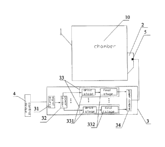
Further, as shown in Figs. 2A, 3 and 4, the semiconductor microwave source 3
includes: a
signal source 31, a power divider 32, N drive amplifiers 33 and a power
combiner 34. The signal
source 31 is configured to generate a first microwave signal. The power
divider 32 includes a first
input end 6 and N output ends 7, in which the first input end 6 of the power
divider 32 is
connected to the signal source 31, power of the first microwave signal is
allocated by the power
divider 32 according to a preset proportion to generate N second microwave
signals with a same
frequency, and the N second microwave signals with the same frequency
correspond to the N
output ends 7 respectively for outputting (i.e. there is one-to-one
correspondence relationship
between the N second microwave signals and the N output ends 7), where, N is
an integer larger
than or equal to 2. The N drive amplifiers 33 are connected to the N output
ends 7 respectively
(i.e. there is one-to-one connection between the N drive amplifiers 33 and the
N output ends 7).
Each drive amplifier 33 is configured to conduct a drive amplification on a
corresponding second
microwave signal. The power combiner 34 includes N input ends 8 and a first
output end 9. The
N input ends 8 are connected to the N drive amplifiers 33 respectively (i.e.
there is one-to-one
connection between the N input ends 8 and the N drive amplifiers 33). The
power combiner 34 is
configured to combine the N second microwave signals after the drive
amplification to obtain a
third microwave signal and to output the third microwave signal via the first
output end 9.
In embodiments of the present disclosure, the structure of the power divider
32 is show in
Fig. 3 and the structure of the power combiner 34 is shown in Fig. 4. The
power divider 32
divides the power of the first microwave signal provided by the signal source
31 according to the
preset proportion, i.e. power of the second microwave signal outputted by each
output end of the
power divider 32 is in the preset proportion. When the preset proportion is 1,
the power of the
first microwave signal provided by the signal source 31 is equally divided by
the power divider
32, i.e. the power of the second microwave signal outputted by each output end
of the power
divider 32 is equal. As shown in Figs. 3 and 4, the power divider 32 may be
used as the power
combiner 34, and the power combiner 34 may also be used as the power divider
32, via
exchanging the position of the input end and the output end.
The power divider 32 and the power combiner 34 may be a waveguide-type power
divider or
a microstrip-type power divider, and the power divider 32 and the power
combiner 34 may be any
9
=
CA 02950450 2016-11-28
type that may realize a power dividing or combining, such as a T-type junction
power divider, a
Wilkinson power divider, a waveguide magic T, a directional coupler, and a
branch-line hybrid
network. Therefore, both the power divider 32 and the power combiner 34 can be
any one of the
T-type junction power divider, the Wilkinson power divider, the waveguide
magic T and the
directional coupler.
As shown in Fig. 2A, the microwave conversion device 5 is connected to the
first output end
9 of the power combiner 34 and the waveguide box 2 respectively. The microwave
conversion
device 5 is configured to feedback the third microwave signal to the waveguide
box 2 so as to
transmit the third microwave signal to the chamber 10. The microwave
conversion device 5 may
be a feed-in device like a probe and an antenna etc. The control device 4 is
configured to control
the signal source 31 to generate the first microwave signal. That is, the
signal source 31 generates
a low-power microwave signal, i.e. the first microwave signal, under the
control of the control
device 4. The first microwave signal is then devided into N second microwave
signals via the
power divider 32 and each second microwave signal is inputted into the
corresponding drive
amplifier 33. The second microwave signals after the drive amplification
conducted by the drive
amplifiers 33 are inputted into the power combiner 34 respectively. After the
power combination,
the microwave signal is fed back into the waveguide box 2 via the microwave
conversion device
5 and is transmited into the chamber 10.
Fig. 2B is a schematic diagram of another semiconductor microwave oven
according to an
embodiment of the present disclosure. As shown in Fig. 2B, the semiconductor
microwave oven
includes: a body 1, N waveguide boxes 2, a semiconductor microwave source 3, a
control device
4 and N microwave conversion devices 5, where, N is an integer larger than or
equal to 2.
The body 1 includes a chamber 10. The N waveguide boxes 2 are set on the body
1. As
shown in Fig. 2B, N is equal to 2, and the two waveguide boxes are
respectively set on the left
and right side of the body 1.
Further, as shown in Figs. 2B and 3, the semiconductor microwave source 3
includes: a
signal source 31, a power divider 32 and N drive amplifiers 33. The signal
source 31 is
configured to generate a first microwave signal such as a low-power microwave
signal. The
power divider 32 includes a first input end 6 and N output ends 7, in which
the first input end 6 of
the power divider 32 is connected to the signal source 31, power of the first
microwave signal is
allocated by the power divider 32 according to a preset proportion to generate
N second
microwave signals with a same frequency, and the N second microwave signals
with the same
= = CA 02950450 2016-11-28
frequency correspond to the N output ends respectively for outputting(i.e.
there is one-to-one
correspondence relationship between the N second microwave signals and the N
output ends 7).
The N drive amplifiers 33 are connected to the N output ends 7 respectively
(i.e. there is
one-to-one connection between the N drive amplifiers 33 and the N output ends
7). Each drive
amplifier 33 is configured to conduct a drive amplification on the
corresponding second
microwave signal.
In embodiments of the present disclosure, the structure of the power divider
32 is shown in
Fig. 3. The power divider 32 divides the power of the first microwave signal
provided by the
signal source 31 according to a preset proportion, i.e. power of the second
microwave signal
outputted by each output end of the power divider 32 is in the preset
proportion. When the preset
proportion is 1, the power of the first microwave signal provided by the
signal source 31 is
equally divided by the power divider 32, i.e. the power of the second
microwave signal outputted
by each output end of the power divider 32 is equal.
The power divider 32 may be a waveguide-type power divider or a microstrip-
type power
divider, and the power divider 32 may be any type that may realize a power
dividing, such as a
T-type junction power divider, a Wilkinson power divider, a waveguide magic T,
a directional
coupler, and a branch-line hybrid network. Therefore, the power divider 32 can
be any one of the
T-type junction power divider, the Wilkinson power divider, the waveguide
magic T and the
directional coupler.
As shown in Fig. 2B, the N microwave conversion devices 5 are correspondingly
connected
to the N drive amplifiers 33 and the waveguide boxes 2 respectively (i.e.
there is one-to-one
connection between the N microwave conversion devices 5 and the N drive
amplifiers 33, and
one-to-one connection between the N microwave conversion devices 5 and the
waveguide boxes
2). Each microwave conversion device 5 is configured to feedback the second
microwave signal
after the drive amplification conducted by the corresponding drive amplifier
33 to the
corresponding waveguide box 2 so as to transmit the second microwave signals
after the drive
amplification to the chamber 10, and to combine the second microwave signals
after the drive
amplification into a high-power microwave signal. The microwave conversion
device 5 may be a
feed-in device like a probe and an antenna etc. The control device 4 is
configured to control the
signal source 31 to generate the first microwave signal. That is, the signal
source 31 generates a
low-power microwave signal, i.e. the first microwave signal, under the control
of the control
device 4. The first microwave signal is then devided into the N second
microwave signals via the
11
= =
CA 02950450 2016-11-28
power divider 32 and the second microwave signals are inputted into each drive
amplifier 33. The
second microwave signals after the drive amplification conducted by the drive
amplifiers 33 are
inputted into the corresponding microwave conversion devices 5 respectively.
The second
microwave signals after the drive amplification are fed back into the
waveguide boxes 2 via the
microwave conversion devices 5 and are transmitted into the chamber 10, and
are finally
combined into a high-power microwave in the chamber 10.
The waveguide box 2 and the microwave conversion device 5 are constructed into
the
microwave input device, and the number of the waveguide boxes 2 is at least 1.
That is, the microwave input device includes at least one waveguide box 2, and
the at least
one waveguide box 2 is set on the body 1. As shown in Fig. 2A, if the number
of the waveguide
box 2 is 1, the semiconductor microwave source 3 further includes a power
combiner 34, and the
microwave input device further includes a microwave conversion device 5,
where, the power
combiner includes N input ends and a first output end, the N input ends are
connected to the N
drive amplifiers respectively, the microwave conversion device is respectively
connected to the
first output end and the waveguide box, the power combiner is configured to
combine the N
second microwave signals after the drive amplification to a third microwave
signal and to output
the third microwave signal via the first output end, and the microwave
conversion device is
configured to feedback the third microwave signal to the waveguide box so as
to transmit the
third microwave signal to the chamber. As shown in Fig. 2B, if the number of
the waveguide
boxes is N, e.g. N is 2, the microwave input device further includes N
microwave conversion
devices 5, where, the N microwave conversion devices are connected to the
corresponding N
drive amplifiers and the corresponding N waveguide boxes respectively, and
each microwave
conversion device is configured to feedback the second microwave signal after
the drive
amplification conducted by the corresponding drive amplifier to the
corresponding waveguide
box so as to transmit the second microwave signals after the drive
amplification conducted by the
N drive amplifiers to the chamber.
Therefore, the semiconductor microwave oven in embodiments of the present
disclosure
includes: a body, a microwave input device, a semiconductor microwave source
and a control
device. The body includes a chamber, and the microwave input device is in
communication with
the chamber. The semiconductor microwave source includes a signal source, a
power divider and
N drive amplifiers. The signal source is configured to generate a first
microwave signal. The
power divider includes a first input end and N output ends, in which the first
input end of the
12
=
CA 02950450 2016-11-28
power divider is connected to the signal source, power of the first microwave
signal is allocated
by the power divider according to a preset proportion to generate N second
microwave signals
with a same frequency, and the N second microwave signals with the same
frequency correspond
to the N output ends for outputting, where, N is an integer larger than or
equal to 2. The N drive
amplifiers are connected to the N output ends respectively. Each drive
amplifier is configured to
conduct a drive amplification on a corresponding second microwave signal and
to input the N
second microwave signal after the drive amplification to the microwave input
device, so as to
transmit the second microwave signal via the microwave input device to the
chamber. The control
device is configured to control the signal source to generate the first
microwave signal.
According to an embodiment of the present disclosure, as shown in Fig. 2A or
2B, the drive
amplifier 33 further includes: a drive component 331, i.e. a drive stage, and
an amplification
component 332, i.e. a final stage. The drive component 331 is configured to
conduct a first drive
amplification on the second microwave signal so as to generate a fourth
microwave signal. The
amplification component 332 is connected to the drive component 331, and
configured to conduct
a second amplification on the fourth microwave signal so as to generate the
second microwave
signal after the drive amplification. In addition, as shown in Fig. 2A, the
number of the drive
components 331 and the number of the amplification components 332 are equal to
the number of
the output ends of the power divider 32 and the number of the input ends of
the power combiner
34.
Power of the first microwave signal is greater than power of the second
microwave signal,
power of the fourth microwave signal is greater than power of the second
microwave signal, and
power of the second microwave signal after the drive amplification is greater
than power of the
fourth microwave signal.
According to an embodiment of the present disclosure, if the power divider 32
is a T-type
junction power divider, as shown in Fig. 5, the low-power first microwave
signal generated by
the signal source 31 is inputted via the first input end 6. Two impedance
transforming lines 322
with 1/4 wavelength (A) are set, and the characteristic impedances are Z02 and
Z03 respectively.
Different power dividing for the outputted second microwave signals is
realized by setting
impedances of Z02 and Z03, and the second microwave signals after dividing are
outputted via
two output ends 7 respectively. The T-type junction power divider may be used
as the power
combiner 34 conversely.
According to another embodiment of the present disclosure, if the power
divider 32 is a
13
CA 02950450 2016-11-28
Wilkinson power divider, as shown in Fig. 6, the low-power first microwave
signal generated by
the signal source 31 is inputted via the input end 6 of the Wilkinson power
divider. Two
impedance transforming lines 322 with 1/4 wavelength are set, and the
characteristic impedances
are Z02 and Z03 respectively, and an isolation resistance 321 is set, so as to
ensure that the two
output ends 7 of the Wilkinson power divider are isolated. If any one of the
output ends 7 is
dismatched, there will be current flows past the isolation resistance 321 and
the power will be
wasted on the isolation resistance 321, which shall not affect the output of
another output end 7.
The two output ends 7 then respectively pass impedance transforming lines 323
with 1/4
wavelength, such that the power dividing is realized. When the power is
equally divided, the
characteristic impedance of the input end is ZO, then Z02= Z03=,5ZO, and the
characteristic
impedance of the impedance transforming lines 323 is ZO. Similarly, the
Wilkinson power divider
may be used as the power combiner 34 conversely.
According to yet another embodiment of the present disclosure, when the power
divider 32 is
a directional coupler, as shown in Fig. 7, it includes two parallel conduction
bands 324, the
coupling is realized via two branch conduction bands 325, and the length and
the interval of the
branch conduction bands 325 are both 1/4 wavelength. The low-power first
microwave signal
generated by the signal source 31 is inputted via an input end 61. In an ideal
situation, the input
end 61 has no reflection, the power inputted is outputted by ends 72 and 73,
and end 64 has no
output, i.e. ends 61 and 64 are isolated with each other. For a situation that
power is equally
divided, the characteristic impedance of the branch conduction bands are
similar with input and
output lines, and the characteristic resistance of the parallel conduction
bands is 1/'µ5 of the
input and output lines. Similarly, the directional coupler may be used as the
power combiner 34
conversely.
In embodiments of the present disclosure, when the number of the outputs of
the power
divider 32 is greater than two, a multi-stage impedance conversion is needed.
For example,
according to a first embodiment of the present disclosure, as shown in Fig. 8,
the low-power first
microwave signal generated by the signal source 31 is inputted via the first
input end 6, and it is
divided into three signals after conducting a first stage impedance
conversion, and finally three
second microwave signals are outputted via three output ends respectively
after conducting a
second stage impedance change.
According to a second embodiment of the present disclosure, as shown in Fig.
9, the
14
CA 02950450 2016-11-28
low-power first microwave signal generated by the signal source 31 is inputted
via the first input
end 6, and it is divided into two signals after conducting a first stage
impedance conversion, then
the two signals are divided into four signals after conducting a second stage
impedance
conversion and a following third stage impedance conversion, and finally four
second microwave
signals are outputted via four output ends respectively.
According to a third embodiment of the present disclosure, as shown in Fig.
10, the
low-power first microwave signal generated by the signal source 31 is inputted
via the first input
end 6, and it is divided into two signals after conducting a first stage
impedance conversion, then
the two signals are divided into four signals after conducting a second stage
impedance
conversion and a following third stage impedance conversion, and then the four
signals are
divided into eight signals after conducting a fourth stage impedance
conversion, and finally eight
second microwave signals are outputted via eight output ends correspondingly.
According to a fourth embodiment of the present disclosure, as shown in Fig.
11, the
low-power first microwave signal generated by the signal source 31 is inputted
via the first input
end 6, and it is divided into two signals after conducting a first stage
impedance conversion, then
the two signals are divided into six signals after conducting a second stage
impedance conversion
and a following third stage impedance conversion, and then the six signals are
divided into twelve
signals after conducting a fourth stage impedance conversion, and finally
twelve second
microwave signals are outputted via twelve output ends correspondingly.
According to Figs. 8 to 11, the low-power first microwave signal generated by
the signal
source 31 is inputted via the first input end 6, and it is divided into two or
three signals after
conducting a first stage impedance conversion, and the two or three signals
are then divided after
conducting a second stage impedance conversion. If the requirement of the
number of the
microwave sources may still not be satisfied, signals may be conducted the
third stage and fourth
stage impedance conversion, will finally be outputted from multiple output
ends 7.
According to an embodiment of the present disclosure, as shown in Fig. 12A or
12B, the
semiconductor microwave source 3 further includes N phase shifters 35. The N
phase shifters 35
are respectively connected between the N output ends 7 and the N drive
amplifiers 33, in which,
each phase shifter 35 is configured to perform a phase adjustment on the
second microwave
signal output by the corresponding output end in the N output ends under the
control of the
control device 4, such that the efficiency of the semiconductor microwave
source is improved.
The phase shifter 35 may be any one of a phase shifter type that may be
suitable for
CA 02950450 2016-11-28
microwave thermal spectrum like a PIN diode phase shifter, a ferrite phase
shifter, and a vector
modulation phase shifter. The phase shifter 35 may also be any one of a loaded-
line phase shifter,
and a switch-line phase shifter.
If the phase shifter 35 is the loaded-line phase shifter, as shown in Fig. 13,
a controllable
reactance element 352 is provided on a uniform transmission line 351 by the
loaded-line phase
shifter, and the reactance element 352 and the transmission line 351 can be
connected parallelly
or seriesly, in which, a phase shift amount may be introduced by controlling
the reactance value
of the reactance element by the the control device 4.
If the phase shifter 35 is the switch-line phase shifter, as shown in Fig. 14
or 15, in which,
Fig. 14 is a schematic diagram of a series-connected switch-line phase
shifter. When switches Si
and S4 are engaged, and S2 and S3 are disengaged, the second microwave signal
is transmitted
via a transmission route li; and when the switch status are opposite, the
switches Si and S4 are
disengaged, and S2 and S3 are engaged, the second microwave signal is
transmitted via a
transmission route 12, a phase change is realized according to the change of
the transmission route.
The phase shifter shown in Fig. 15 is a parallel switch-line phase shifter.
When the switches S1
and S4 are engaged, the transmission route 11 is a short circuit, and the
switches S2 and S3 are
disengaged, the second microwave signal is transmitted via the transmission
route 12, otherwise is
transmitted via the transmission route 1 A switch may also be replaced by a
diode, as shown in
Fig. 16.
In conclusion, according to the semiconductor microwave oven in the
embodiments of the
present disclosure, the number of the signal source for generating microwave
signals is 1.
Therefore, multiple-route semiconductor power sources share a same signal
source, such that the
multiple-route semiconductor power sources can be ensured to work under a same
frequency, and
thus realizing a high-efficiency power output, and ensuring the heating
efficiency of the
semiconductor microwave oven.
According to the semiconductor microwave oven in the embodiments of the
present
disclosure, the second microwave signals with the same frequency outputted by
the N output ends
of the power divider share a same signal source so as to enaure to work in the
same frequency,
such that a high-efficiency power output is realized and a heating efficiency
is ensured. In
addition, the structure of the semiconductor microwave oven in the embodiments
of the present
disclosure is more simple and compact, and it is cost-saving.
In addition, a semiconductor microwave source of a semiconductor microwave
oven is
16
CA 02950450 2016-11-28
further provided in embodiments of the present disclosure. The semiconductor
microwave source
includes: a signal source, a power divider and N drive amplifiers. The signal
source is configured
to generate a first microwave signal. The power divider includes a first input
end and N output
ends, in which the first input end of the power divider is connected to the
signal source, power of
the first microwave signal is allocated by the power divider according to a
pre-set proportion to
generate N second microwave signals with a same frequency, and the N second
microwave
signals with the same frequency correspond to the N output ends respectively
for outputting,
where, N is an integer larger than or equal to 2. The N drive amplifiers are
connected to the N
output ends respectively. Each drive amplifier is configured to conduct a
drive amplification on a
corresponding second microwave signal and to input the second microwave signal
after the drive
amplification to the microwave input device, so as to transmit the second
microwave signal after
the drive amplification via the microwave input device to the chamber. The
signal source is
configured to generate the first microwave signal under a control of a control
device of the
semiconductor microwave oven.
In embodiments of the present disclosure, the microwave input device includes
at least one
waveguide box, and the at least one waveguide box is set on the body. If the
number of the
waveguide box is 1, the semiconductor microwave source further includes a
power combiner, and
the microwave input device further includes a microwave conversion device,
where, the power
combiner includes N input ends and a first output end, the N input ends are
connected to the N
drive amplifiers respectively, the microwave conversion device is respectively
connected to the
first output end and the waveguide box, the power combiner is configured to
combine the N
second microwave signals after the drive amplification to obtain a third
microwave signal and to
output the third microwave signal via the first output end, and the microwave
conversion device
is configured to feedback the third microwave signal to the waveguide box so
as to transmit the
third microwave signal to the chamber. If the number of the waveguide boxes is
N, the
microwave input device further includes N microwave conversion devices, the N
microwave
conversion devices are connected to the corresponding N drive amplifiers and
the corresponding
N waveguide boxes respectively, and each microwave conversion device is
configured to
feedback the second microwave signal after the drive amplification conducted
by the
corresponding drive amplify to the corresponding waveguide box so as to
transmit the second
microwave signals after the drive amplification conducted by the N drive
amplifiers to the
chamber.
17
CA 02950450 2016-11-28
Specifically, according to an embodiment of the present disclosure, as shown
in Fig. 2A,
when the number of the waveguide box is 1, the above semiconductor microwave
source 3 of the
semiconductor microwave oven includes: a signal source 31, a power divider 32,
N drive
amplifiers 33 and a power combiner 34. The signal source 31 is configured to
generate a first
microwave signal. The power divider 32 includes a first input end 6 and N
output ends 7, in
which the first input end 6 of the power divider 32 is connected to the signal
source 31, power of
the first microwave signal is allocated by the power divider 32 according to a
pre-set proportion
to generate N second microwave signals with a same frequency, and the N second
microwave
signals with the same frequency correspond to the N output ends 7 for
outputting, where, N is an
integer larger than or equal to 2. The N drive amplifiers 33 are connected to
the N output ends 7
respectively. Each drive amplifier 33 is configured to conduct a drive
amplification on a
corresponding second microwave signal. The power combiner 34 includes N input
ends 8 and a
first output end 9. The N input ends 8 and the N drive amplifiers 33 are
correspondingly
connected. The power combiner 34 is configured to combine the N second
microwave signals
after the drive amplification to obtain a third microwave signal and to output
the third microwave
signal to the microwave conversion device 5 via the first output end 9, and
then the third
microwave signal is fed into the waveguide box 2 by the microwave conversion
device 5, so as to
transmit the third microwave signal to the chamber 10. The signal source 31 is
configured to c
generate the first microwave signal under a control of the control device 4 of
the semiconductor
microwave oven.
According to another embodiment of the present disclosure, when the number of
the
waveguide boxes is N, e.g. as shown in Fig. 2B, when the number of the
waveguide box is 2, the
above semiconductor microwave source 3 of the semiconductor microwave oven
includes: a
signal source 31, a power divider 32, and N drive amplifiers 33. The signal
source 31 is
configured to generate a first microwave signal, e.g. a low-power microwave
signal. The power
divider 32 includes a first input end 6 and N output ends7, in which the first
input end 6 of the
power divider 32 is connected to the signal source 31, power of the first
microwave signal is
allocated by the power divider 32 according to a pre-set proportion to
generate N second
microwave signals with a same frequency, and the N second microwave signals
with the same
frequency correspond to the N output ends respectively for outputting, where,
N is an integer
larger than or equal to 2. The N drive amplifiers 33 are connected to the N
output ends 7
respectively. Each drive amplifier 33 is configured to conduct a drive
amplification on a
18
CA 02950450 2016-11-28
corresponding second microwave signal. The N second microwave signals after
the drive
amplification are sent to the corresponding microwave input devices 5 by the N
drive amplifiers
33 respectively, and then are fed into the corresponding waveguide boxes 2 by
the N microwave
input devices 5, so as to transmit via the microwave input device to the
chamber 10; where, the
signal source 31 is configured to generate the first microwave signal under a
control of the
control device 4 of the semiconductor microwave oven.
The power divider 32 and the power combiner 34 may be a waveguide-type power
divider or
a microstrip-type power divider, and the power divider 32 and the power
combiner 34 may be any
type that may realize a power dividing or combining, such as a T-type junction
power divider, a
Wilkinson power divider, a waveguide magic T, a directional coupler, and a
branch-line hybrid
network. Therefore, both the power divider 32 and the power combiner 34 can be
any one of the
T-type junction power divider, the Wilkinson power divider, the waveguide
magic T and the
directional coupler.
According to an embodiment of the present disclosure, as shown in Fig. 2A or
2B, the drive
amplifier 33 further includes: a drive component 331 and an amplification
component 332. The
drive component 331 is configured to conduct a first drive amplification on
the second
microwave signal so as to generate a fourth microwave signal. The
amplification component 332,
is connected to the drive component, and is configured to conduct a second
amplification on the
fourth microwave signal so as to generate the second microwave signal after
the drive
amplification. In addition, as shown in Fig. 2A, the number of the drive
components 331 and the
number of the amplification components 332 are equal to the number of the
output end of the
power divider 32 and the number of the input end of the power combiner 34.
Power of the first microwave signal is greater than power of the second
microwave signal,
power of the fourth microwave signal is greater than power of the second
microwave signal, and
power of the second microwave signal after the drive amplification is greater
than power of the
fourth microwave signal.
Further, according to an embodiment of the present disclosure, as shown in
Fig. 12A or 12B,
the above semiconductor microwave source of the semiconductor microwave oven
further
includes N phase shifters 35. The N phase shifters 35 are respectively
connected between the N
output ends 7 and the N drive amplifiers 33, in which, each phase shifter 33
is configured to
perform a phase adjustment on the second microwave signal output by the
corresponding output
end in the N output ends under the control of the control device 4, such that
the efficiency of the
19
=
CA 02950450 2016-11-28
semiconductor microwave source is improved.
The phase shifter is any one of a PIN diode phase shifter, a ferrite phase
shifter, a vector
modulation phase shifter, a loaded-line phase shifter, and a switch-line phase
shifter.
According to the semiconductor microwave source of the semiconductor microwave
oven in
the embodiments of the present disclosure, the second microwave signals with
the same
frequency outputted respectively by the N output ends of the power divider
share a same signal
source so as to enaure to work in the same frequency, such that a high-
efficiency power output is
realized and a heating efficiency is ensured. In addition, the structure of
the semiconductor
microwave oven in the embodiments of the present disclosure is more simple and
compact, and it
is cost-saving.
In the description of the present specification, reference throughout this
specification to "an
embodiment," "some embodiments," "one embodiment", "another example," "an
example," "a
specific example," or "some examples," means that a particular feature,
structure, material, or
characteristic described in connection with the embodiment or example is
included in at least one
embodiment or example of the present disclosure. Thus, the appearances of the
above phrases in
various places throughout this specification are not necessarily referring to
the same embodiment
or example of the present disclosure. Furthermore, the particular features,
structures, materials, or
characteristics may be combined in any suitable manner in one or more
embodiments or
examples.
Although explanatory embodiments have been shown and described, it would be
appreciated
by those skilled in the art that the above embodiments cannot be construed to
limit the present
disclosure, and changes, alternatives, and modifications can be made in the
embodiments without
departing from spirit, principles and scope of the present disclosure.
20