Note: Descriptions are shown in the official language in which they were submitted.
CA 02952423 2016-12-14
WO 2015/195330 PCT/US2015/033914
TIME DIVISION MULTIPLEXING (TDM) AND WAVELENGTH DIVISION
MULTIPLEXING (WDM) SENSOR ARRAYS
BACKGROUND OF THE INVENTION
Field of the Invention
[0001] Embodiments of the present invention generally relate to
interrogation of
optical components and, more particularly, to techniques and apparatus for
avoiding
overlap of reflections from different arrays of optical elements along the
same
waveguide when interrogated using wavelength-swept light.
Description of the Related Art
[0on] Many optical components have a characteristic wavelength that may be
found by interrogating the optical component with an optical source capable of
producing light at various wavelengths over a fixed range or bandwidth. For
example, fiber Bragg gratings (FBGs) (typically formed by photo-induced
periodic
modulation of the refractive index of an optical waveguide core) are highly
reflective
to light having wavelengths within a narrow bandwidth centered at a wavelength
generally referred to as the Bragg wavelength. Because light having
wavelengths
outside this narrow bandwidth is passed without reflection, Bragg wavelengths
can
be determined by interrogating a Bragg grating with a light source swept
across a
bandwidth that includes the Bragg wavelength and monitoring the reflected
optical
power spectrum at a receiver unit. Because Bragg wavelengths are dependent on
physical parameters, such as temperature and strain, Bragg gratings can be
utilized
in optical sensor systems to measure such parameters.
[0003] In these and a wide range of other types of optical systems, the
measurement of a characteristic wavelength of an optical component to great
accuracy (and/or with great repeatability) is important to system performance.
Two
significant parameters determining the error of any such measurement are the
signal-to-noise ratio (SNR) and effective integration time of the measuring
system.
SNR is dependent of many factors including received optical power, optical-
source
noise, and receiver noise. The effective integration time is dependent on
overall
1
CA 02952423 2016-12-14
WO 2015/195330 PCT/US2015/033914
averaging time and the proportion of that time which is producing useful
signals at
the receiver unit. Improving these two parameters can improve characteristic
wavelength measurement repeatability and accuracy.
[0004] Conventional swept-wavelength Bragg grating interrogators are
limited in
the number of sensors that can be interrogated on a single fiber by the
optical
bandwidth of the source because only wavelength division multiplexing (WDM) is
used to interrogate the sensors. Many of the applications using Bragg grating
sensors can be improved by increasing the number of sensors in the system.
[0005] In some cases, this problem has been addressed by increasing the
optical
bandwidth of the light source to enable more sensors to be multiplexed on the
optical
fiber using WDM.
[0006] In other cases, a swept-wavelength interferometry technique has been
used. This technique may allow time division multiplexing (TDM) of grating
sensors;
however, the swept-wavelength interferometry technique may suffer from a
limited
spatial window range as well as limited wavelength resolution. In yet another
approach, time-gated lasers have been used to TDM Bragg grating sensors.
SUMMARY OF THE INVENTION
[0007] Embodiments of the present invention generally relate to
interrogating sets
of optical elements having characteristic wavelengths spanning a sweep range
while
avoiding overlapping reflections from the different sets at a receiver when
performing
a wavelength sweep. Some embodiments may include delay mechanisms between
the different sets of optical elements, thereby allowing the sets to be
physically
located in close proximity to one another.
[0oos] One embodiment of the present invention is a method for optical
interrogation. The method generally includes introducing a pulse of light, by
an
optical source, into an optical waveguide to interrogate at least first and
second sets
of optical elements by performing a sweep of wavelengths over a period of the
pulse,
wherein the optical elements within each set have different characteristic
wavelengths and wherein the first and second sets are separated in time such
that a
2
CA 02952423 2016-12-14
WO 2015/195330 PCT/US2015/033914
first time window over which light is reflected form the optical elements in
the first set
and reaches a receiver does not overlap with a second time window over which
light
is reflected from the optical elements in the second set and reaches the
receiver;
and processing the reflected light to determine one or more parameters
corresponding to the optical elements.
[0009] Another embodiment of the present invention is an apparatus for
optical
interrogation. The apparatus generally includes an optical waveguide; an
optical
source configured to introduce a pulse of light into the optical waveguide to
interrogate at least first and second sets of optical elements by performing a
sweep
of wavelengths over a period of the pulse, wherein the optical elements within
each
set have different characteristic wavelengths; a receiver, wherein the first
and
second sets are separated in time such that a first time window over which
light is
reflected from the optical elements in the first set and reaches the receiver
does not
overlap with a second time window over which light is reflected from the
optical
elements in the second set and reaches the receiver; and a processing system
configured to process the reflected light to determine one or more parameters
corresponding to the optical elements.
[0olo] Yet another embodiment of the present invention is a system for
sensing
one or more downhole parameters. The system generally includes a wellbore; an
optical waveguide at least partially disposed in the wellbore; an optical
source
configured to introduce a pulse of light into the optical waveguide by
performing a
sweep of wavelengths over a period of the pulse; at least first and second
sets of
optical elements disposed along the optical waveguide, wherein the optical
elements
within each set have different characteristic wavelengths; a receiver, wherein
the first
and second sets are separated in time such that a first time window over which
light
is reflected from the optical elements in the first set and reaches the
receiver does
not overlap with a second time window over which light is reflected from the
optical
elements in the second set and reaches the receiver; and a processing system
configured to process the reflected light to determine the one or more
downhole
parameters corresponding to the optical elements.
3
CA 02952423 2016-12-14
WO 2015/195330 PCT/US2015/033914
BRIEF DESCRIPTION OF THE DRAWINGS
[0011] So that the manner in which the above recited features of the
present
invention can be understood in detail, a more particular description of the
invention,
briefly summarized above, may be had by reference to embodiments, some of
which
are illustrated in the appended drawings. It is to be noted, however, that the
appended drawings illustrate only typical embodiments of this invention and
are
therefore not to be considered limiting of its scope, for the invention may
admit to
other equally effective embodiments.
[0012] FIG. 1A illustrates an example transmissive optical sensor system
with
wavelength sweep control, in accordance with embodiments of the present
invention;
[0013] FIG. 1B illustrates an example reflective optical sensor system with
wavelength sweep control, in accordance with embodiments of the present
invention;
[0014] FIG. 2 illustrates an example wavelength sweeping optical source
utilizing
a tunable filter, in accordance with embodiments of the present invention;
[0015] FIG. 3 illustrates example interrogation of time division
multiplexed
(TDMed) and effectively wavelength division multiplexed (WDMed) sensors on a
single fiber using a fast-swept optical source, in accordance with embodiments
of the
present invention;
[0016] FIG. 4 illustrates example signal return times from three adjacent
arrays of
effectively WDMed optical sensors arranged in increasing wavelength order
within
each array, interrogated with a sweep of increasing wavelength from a fast-
swept
optical source, in accordance with embodiments of the present invention;
[0017] FIG. 5 illustrates example signal return times from two adjacent
arrays of
effectively WDMed optical sensors arranged in increasing wavelength order
within
each array and separated by an empty section of fiber, interrogated with a
sweep of
increasing wavelength from a fast-swept optical source, in accordance with
embodiments of the present invention;
[0018] FIG. 6A illustrates an example arrangement of sets of TDMed and
4
CA 02952423 2016-12-14
WO 2015/195330 PCT/US2015/033914
effectively WDMed sensors limited in closeness along the optical waveguide by
the
return time of the signals from the sensor sets, in accordance with
embodiments of
the present invention;
[0019] FIG. 6B illustrates an example arrangement of sets of TDMed and
effectively WDMed sensors having a delay coil disposed between each sensor
set,
in accordance with embodiments of the present invention;
[0020] FIG. 60 illustrates an example arrangement of sets of TDMed and
effectively WDMed sensors having a plurality of delay loop-backs disposed
between
each sensor set in accordance with embodiments of the present invention;
[0021] FIG. 7 is a flow diagram of example operations for interrogating
multiple
sets of optical elements, in accordance with embodiments of the present
invention;
and
[0022] FIG. 8 is a schematic cross-sectional view of an example wellbore
with
multiple sensor arrays, in accordance with embodiments of the present
invention.
DETAILED DESCRIPTION
[0023] Embodiments of the present invention provide techniques and
apparatus
for interrogating arrays of time division multiplexed (TDMed) and effectively
wavelength division multiplexed (WDMed) optical sensors having characteristic
wavelengths spanning a sweep range while avoiding overlapping reflections from
the
different arrays as received at a receiver when performing a wavelength sweep.
Avoiding overlap of reflections from different arrays of optical sensors may
entail
providing an effective time separation (e.g., a corresponding length of
optical fiber)
between arrays, such that reflections from one array do not overlap with
reflections
from another array. Some embodiments may include delay mechanisms between the
different arrays of optical sensors, thereby allowing the arrays to be
physically
located in close proximity to one another. As used herein, the phrase
"physically
located in close proximity" generally refers to the distance between two
arrays being
shorter than a straight length of optical fiber (or other waveguide) having a
round-trip
delay equivalent to the effective time separation.
CA 02952423 2016-12-14
WO 2015/195330 PCT/US2015/033914
AN EXAMPLE OPTICAL SENSOR SYSTEM
[0024] FIG. 1A illustrates an example optical sensor system 100 utilizing
wavelength sweep control in accordance with one embodiment of the present
invention. As illustrated, the system 100 may include a swept-wavelength
optical
source 110, one or more transmissive optical elements 120 having one or more
spectral features of interest (e.g., a characteristic wavelength), and a sweep
control
unit 140.
[0025] The swept-wavelength optical source 110 produces optical radiation
at
wavelengths and over wavelength ranges (bandwidths) under the control or
influence of the sweep control unit 140. The elements 120 may be interrogated
with
optical radiation from the optical source 110 that is swept across a spectral
range
including the spectral features of interest. The elements 120 may be sensitive
to
parameters (e.g., temperatures, pressures, and strain) that affect the
attenuation of
particular wavelengths of light transmitted through the elements 120 in a
known
manner.
[0026] As illustrated in FIG. 2, one embodiment of the optical source 110
may
include a broadband source 112 and a tunable filter 114 that may be controlled
by
the sweep control unit 140. For example, the sweep control unit 140 may
control the
tunable filter 114 to adjust a wavelength range (or band) to pass with little
or no
attenuation while blocking wavelengths outside the range. For other
embodiments,
the optical source 110 may include a light source that can be controlled to
generate
optical signals of different wavelengths, such as a tunable laser.
[0027] Referring back to FIG. 1A, a receiver 130 may include any suitable
combination of optical, opto-electronic, and electronic components to process
light
signals transmitted through the elements 120. Thus, the receiver 130 may be
able to
generate information about the corresponding parameters, based on the timing
of
the received light signals and any shifts therein. The receiver 130 may
include any
suitable combination of components that converts optical signals to electrical
signals,
filters, and samples. As an example, for one embodiment, the receiver may
include
an optical PIN diode (i.e., having a lightly doped near intrinsic
semiconductor region
6
CA 02952423 2016-12-14
WO 2015/195330 PCT/US2015/033914
between a p-type semiconductor region and an n-type semiconductor region),
transimpedance amplifier, analog filter, analog-to-digital converter, digital
filter, and
processing unit (e.g., an embedded processor, industrial or personal computer)
for
wavelength determination.
[0028] As illustrated, the sweep control unit 140 may receive, as input,
one or
more signals from one or more points in the receiver 130 and, in response, may
output signals that influence the sweep of the optical source 110. Examples of
typical parameters that the sweep control unit may influence include, but are
not
limited to, source wavelength, source wavelength sweep range, sweep rate,
and/or
source optical output power. These influences may include discontinuous or
continuous changes in such parameters, for example, multiple sweep bands. The
sweep control unit signals can influence a sweep in progress and/or influence
future
sweeps, as described in greater detail below.
[0029] The sweep control unit 140 may be implemented using any suitable
processing logic, such as an embedded controller, a programmable logic
controller
(PLC) or personal computer (PC). While shown as a separate component in the
Figures, for some embodiments, the sweep control unit 140 may be integrated
into,
or be an integral function of the receiver 130, the source 110, and/or both.
[0030] As illustrated in FIG. 1B, similar techniques may be applied to a
system
utilizing reflective sensor elements 122, such as Bragg gratings, with the
spectral
feature of the light reflected dependent upon a sensed parameter. Each Bragg
grating may be interrogated by sweeping across a corresponding wavelength
range
chosen to contain the characteristic wavelength A, accounting for the maximum
deviations in center wavelengths (areas of peak reflection) expected over the
entire
range of measured parameters and over time. During this interrogation,
response
signals are monitored by the receiver 130 in order to determine the time of
the
response signals, which may be used to determine the characteristic wavelength
of
the sensor element and, thus, the value of the sensed parameter.
[0031] Interrogating optical signals from the source 110 may be directed to
the
7
CA 02952423 2016-12-14
WO 2015/195330 PCT/US2015/033914
reflective sensor elements 122 via a bidirectional coupler 124 that also
directs
reflected response signals to the receiver 130. A splitter 123 may also direct
a
portion of the interrogating optical signals to a reference element 116,
allowing the
receiver 130 to monitor optical signals produced by the optical source 110
(e.g., the
actual wavelength and power). For some embodiments, the reference element 116
may be used to measure the wavelength versus the time of the sweep. The
wavelength-versus-time measurement may be used to correlate return signal
times
of light reflected from the sensor elements 122 with wavelengths in order to
determine a value of a sensed parameter. For example, the reference element
116
may be a Fabry-Perot etalon, a gas absorption cell, etc.
EXAMPLE FAST SWEPT INTERROGATION
[0032] Wavelength division multiplexing (WDM) systems are typically limited
in
the number of sensors that can be interrogated on a single fiber. However,
using a
fast-sweep tunable optical source may increase the number of sensors than can
be
combined on the fiber, thereby allowing distinguishing among signals from the
sensors based on the timing of the received signals and the sweep and, thus,
effectively providing for both WDM and time division multiplexing (TDM) on the
fiber.
[0033] FIG. 3 illustrates example interrogation of TDMed and effectively
WDMed
sensors on a single fiber using a fast-swept tunable optical source, in
accordance
with embodiments of the present invention. As illustrated in FIG. 3, a tunable
optical
source, such as source 110 (e.g., a tunable laser or amplified spontaneous
emission
(ASE) source with a tunable filter) may be coupled to an optical waveguide 302
(e.g.,
an optical fiber) containing multiple optical elements (e.g., fiber Bragg
grating (FBG)
sensors) 322a...i to be interrogated by the optical source 110. The optical
elements
322a...i may have characteristic wavelengths within the output wavelength
capabilities of the optical source 110. An optical coupler, such as optical
coupler
124, may route light reflected by the optical elements 322 to a receiver, such
as
receiver 130.
[0034] The receiver 130, or a separate processing unit, may be configured
to
process (e.g., demodulate) received signals from the optical elements 322a...i
based
8
CA 02952423 2016-12-14
WO 2015/195330 PCT/US2015/033914
on the times at which the signals are received, the sweep rate of source 110,
and the
relative distances of the optical elements 322a...i from the optical source
110 and
the receiver 130 (i.e., time-of-flight). The receiver 130 may convert the
optical
signals to electrical signals for further processing. The tunable optical
source 110
may have a fast sweep rate such that a sweep of the optical spectrum is
completed
in only a fraction of the time that it takes the light to travel down the
optical
waveguide 302 to the furthest optical element in the system, for example
optical
element 322i shown in FIG. 3, and be reflected back to the receiver 130 (i.e.,
the
round-trip time). For some embodiments, this sweep is accomplished in a period
less than a round-trip time to the closest optical element along the
waveguide. After
completing a sweep of the desired optical spectrum, the optical source 110 may
be
turned off or idled by outputting a wavelength which will not be reflected by
any of
the optical elements 322. In some embodiments, the optical source 110 may emit
a
chirped pulse of light.
[0035] The sweep time of the optical source 110 is used to define a sweep
window within which multiple optical elements 322 can be multiplexed using
WDM,
so to speak. The optical elements within each set are effectively WDMed by
having
different characteristic wavelengths that reflect light at different times
according to
their individual distance along the fiber and the parameters of the wavelength
sweep
function (e.g., the sweep rate). The sweep time of the optical source 110,
along with
the wavelength direction of the sweep (e.g., short wavelengths to long
wavelengths
or long wavelengths to short wavelengths), the distance to and spacing of the
optical
elements in the WDMed set, and the ordering of the characteristic wavelengths
of
the optical elements in the set define a time/distance window of the light
received
from (e.g., reflected by) the optical elements in the set. For example, the
time at
which light may be received from an optical element within the set may
correspond
to a distance of the optical element from the optical source, as well as the
characteristic wavelength of the optical element and when that wavelength
occurs
during the sweep (which may depend on the direction of the sweep). Therefore,
a
window may be defined for each set that includes the spread, in time or
distance, of
the light signals received from the optical elements within the set.
9
CA 02952423 2016-12-14
WO 2015/195330 PCT/US2015/033914
[0036]
Therefore, in order for optical elements 322 to be multiplexed on the
optical waveguide 302 using WDM, the optical elements may have different
characteristic wavelengths. For example, as illustrated in FIG. 3, optical
elements
322a, 322b, and 322c may be located within the sweep window and have
characteristic wavelengths A_1, A_2, and A_3, where A_1, A_2, and A_3 are each
different wavelengths. In this case, optical elements 322a, 322b, and 322c may
be
effectively WDMed on the optical waveguide 302. The receiver 130 may
distinguish
among signals received from the optical elements 322a, 322b, and 322c based on
the time at which the signals are received, which is a function of the sweep
parameters.
[0037]
Additional optical elements can be multiplexed using TDM as long as they
are outside the sweep windows of other sensors with the same characteristic
wavelengths. For example, as illustrated in FIG. 3, optical elements 322d,
322e, and
322f may be located outside the sweep window of optical elements 322a, 322b,
and
322c. Optical elements 322d, 322e, and 322f may therefore have characteristic
wavelengths A_1, A_2, and A_3, and the optical sensors may be TDMed to
distinguish therebetween. Similarly, optical elements 322g, 322h, and 322i may
be
outside the sweep windows of optical elements 322a, 322b, 322c, 322d, 322e,
and
322f. Optical elements 322g, 322h, and 322i may therefore also have
characteristic
wavelengths A_1, A_2, and A_3, and the optical sensors may be TDMed to
distinguish therebetween. In certain embodiments, optical elements 322d-322i
may
have characteristic wavelengths different than the first set of optical
elements
(e.g., A_4 - A_9).
[0038] In
certain embodiments, the optical elements may be in arranged in order
of increasing or decreasing order of characteristic wavelength. In
some
embodiments, the optical elements may be arranged in any order of
characteristic
wavelengths (e.g., randomly). In certain embodiments, optical elements of the
second set may be arranged in the same order or the reverse order of
characteristic
wavelengths of the optical elements in the first set. In certain embodiments,
optical
elements of the second set may be arranged in any order of characteristic
CA 02952423 2016-12-14
WO 2015/195330 PCT/US2015/033914
wavelengths (e.g., randomly).
[0039] In some embodiments, the sweep rate may be about 400 kHz,
corresponding to a 2.5 ps sweep time and sweep distance of 500 m in an optical
fiber. In some embodiments, the sweep rate may be about 1 MHz or higher. The
resolution of the sweep or sweep time may be dependent on the sample rate of
the
receiver 130. For example, for a 1 MHz sweep rate, a receiver may sample with
a
13-bit data acquisition card.
[0040] Using the above-described approaches, multiple sets of optical
elements
can be multiplexed on the fiber, greatly increasing the number of sensors in
the
sensing system that can be distinguished. If the wavelength sweep range is
reduced
to cover the operational wavelength range of just one optical element, then
the
system may become a TDM-only system.
EXAMPLE OPTICAL SENSOR ARRAY ARRANGEMENTS
[0041] As described above, a sweep window generally refers to the time (or
corresponding distance) over which all of the sensor signal reflections from a
single
set of (effectively wavelength division multiplexed) sensors are spread when
travelling back to the receiver. Thus, the optical sensors in each set may be
effectively multiplexed on the fiber using WDM (based on the wavelength sweep
and
the different characteristic wavelengths within the set), and the sets of
optical
sensors may be multiplexed using TDM (based on the timing of the received
signals
reflected from the optical elements).
[0042] The ability to time domain multiplex optical sensors in an array of
such
sensors may be limited by the time spread of return signals from each array of
effectively WDMed sensors. For example, if two adjacent sets of sensors are
interrogated with a fast-swept tunable-wavelength source and positioned too
closely
together, return signals from the sensors may overlap. FIG. 4 is a graph 400
of
example signal return times from three adjacent arrays of effectively WDMed
optical
sensors (labeled WDM Set 1, WDM Set 2, and WDM Set 3), where the arrays have
no significant space therebetween. To generate the data in FIG. 4, each array
has
11
CA 02952423 2016-12-14
WO 2015/195330 PCT/US2015/033914
20 optical sensors, each having a different characteristic wavelength spaced
over 10
meters. The
optical sensors within each array are arranged in increasing
wavelength order (i.e., from shortest wavelength to longest wavelength) and
are
interrogated using a 1.9 ps linear sweep of increasing wavelength from a fast-
swept
tunable-wavelength source. As illustrated, return signals from adjacent arrays
of
sensors overlap in time. This overlap may make it difficult to determine from
which
array and, thus, from which sensor the return signal was reflected.
[0043]
Avoiding such overlap of return signals may limit how closely the sensors
can be spaced in a uniform array or force the sensors to be clustered in sets
of WDM
sensors with larger gaps between adjacent sets of sensors multiplexed by TDM.
Either case may result in an arrangement of undesirable sensor spacings for
certain
sensing applications. For example, in downhole oil and gas applications¨where
the
sensors are typically deployed in series along production tubing disposed in a
wellbore, a large number of closely spaced (e.g., 1 to 20 m) sensors may be
utilized
to cover several kilometers of well length.
[0044]
While this sensor spacing problem may be solved by using multiple optical
fibers to cover the gaps between sensors, the use of multiple fibers may not
be
feasible for some applications, perhaps due to cost or limited fiber
availability (e.g.,
due to a limited number of high pressure feedthroughs). Accordingly, what is
needed are techniques and apparatus for avoiding overlap of reflections from
different sets of optical sensors disposed along the same waveguide when
interrogated using wavelength-swept light and for allowing the sets to be
physically
located in close proximity to one another.
[0045]
Embodiments of the present invention utilize an empty length of optical
fiber or other waveguide between sets of effectively WDMed sensors in an
effort to
avoid overlap of reflections from the different sets. As used herein, an empty
length
of optical fiber generally refers to a length of optical fiber without any
optical sensors.
[0046] In
contrast with FIG. 4, FIG. 5 is a graph 500 of example signal return
times from two adjacent arrays of effectively WDMed optical sensors separated
by
12
CA 02952423 2016-12-14
WO 2015/195330 PCT/US2015/033914
an empty length of optical fiber between the two arrays (labeled WDM Set 1 and
WDM Set 2). Like FIG. 4, each array has 20 optical sensors, each having a
different
characteristic wavelength, spaced over 10 m to generate the data in FIG. 5.
However, the arrays are spaced 200 meters apart along the optical fiber. The
optical
sensors within each array are arranged in increasing wavelength order and are
interrogated using a 1.9 ps linear sweep of increasing wavelength from a fast-
swept
tunable wavelength source, As illustrated, the return signals from the first
and
second sets of sensors do not overlap in time.
[0047] FIG. 6A illustrates an example arrangement 600a for solving the
problem
of time overlapping return signals from adjacent WDM sensor sets when
interrogated
with a fast-swept tunable-wavelength source, similar to the arrangement of WDM
Sets 1 and 2 in FIG. 5. The arrangement 600a has a number of effectively WDMed
and TDMed sensors 322 deployed along an optical fiber to perform sensing of
one or
more parameters (e.g., temperature or pressure). Multiple WDMed sensors 322
may
be grouped into a number of sets, with each set separated by an empty length
of
optical fiber 602 in an effort to avoid the time overlap, given the speed of
light in this
optical fiber and the corresponding round-trip delay provided by this length.
As
illustrated in FIG. 6A the empty length of optical fiber 602 is interposed
between a
first set of sensors 322 (WDM Set 1) and a second set of sensors 322 (WDM Set
2)
to separate reflected signals from the first and second sets of sensors in
time (as
depicted in the graph 500 of FIG. 5, for example), so that a receiver may
determine
from exactly which sensor 322 a reflected signal was returned.
[0048] As illustrated in the arrangement 600a of FIG. 6A, the empty length
of
optical fiber 602 may be a straight length of optical fiber, without any
substantial
bends, turns, etc. However, such a straight section of optical fiber precludes
adjacent sets of optical sensors from being physically located any closer
together
than the length of the empty, straight section and may also prevent the
placement of
sensors in a desired position. FIGs. 6B and 60 illustrate example arrangements
600b and 600c, respectively, for solving this problem by employing particular
delay
mechanisms between adjacent arrays of optical sensors.
13
CA 02952423 2016-12-14
WO 2015/195330 PCT/US2015/033914
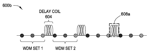
[0049] FIG. 6B illustrates an example arrangement 600b of sensor arrays
using a
delay coil 604 as the delay mechanism, which may be positioned between any two
adjacent sensor arrays as desired. The delay coil 604 may be configured such
that
reflected light from a first set of sensors (e.g., WDM Set 1) as received by
receiver
130 does not overlap with reflected light from a second set of sensors (e.g.,
WDM
Set 2) at the receiver. For example, delay coil 604 may comprise a length of
optical
fiber wound in coils with an optical distance greater than or equal to the
effective
time separation to avoid time overlap of reflected signals from the different
sets,
given the speed of light in the delay coil and the corresponding round-trip
delay
provided by this length of optical fiber. The delay coil 604 permits the first
and
second sets of sensors to be physically located closer together than a
straight length
of optical fiber having a round-trip delay equivalent to the effective time
separation
(e.g., empty, straight section of optical fiber 602 in FIG. 6A).
[0050] In an embodiment, the delay coil 604 may be mounted or otherwise
disposed in a housing 608a, which may provide protection for the delay coil
604.
The housing 608a may be coupled to a portion of an area in which the
arrangement
600b is deployed. For example, in a downhole deployment, the housing 608a may
be coupled (e.g., welded) to a sensing cable, such that the housing provides a
continuous pressure barrier to the outside environment.
[0051] FIG. 60 illustrates an example arrangement 600c of optical sensor
arrays
using an optical fiber looped back and forth multiples times to form a delay
loop-back
605 as a delay mechanism. The delay loop-back 605 may be located between any
two adjacent sensor arrays as desired. The delay loop-back 605 may consist of
a
length of optical fiber with an optical distance greater than or equal to the
effective
time separation to avoid time overlap of reflected signals from the different
sets,
given the speed of light in the loop-back and the corresponding round-trip
delay
provided by this length of optical fiber. Similar to the delay coil 604, the
delay loop-
back 605 also permits the first and second sets of sensors to be physically
located
closer together than a straight length of optical fiber having a round-trip
delay
equivalent to the effective time separation (e.g., empty, straight section of
optical
14
CA 02952423 2016-12-14
WO 2015/195330 PCT/US2015/033914
fiber 602 in FIG. 6A), but avoids overlapping signal reflections therefrom as
described above.
[0052] The delay loop-back 605 may be housed, at least partially, in a
housing
608, which may provide protection for the loop-back. For example, the entire
delay
loop-back 605 may be disposed in a housing 608b, or the turns 606 for at least
one
end of the delay loop-back 605 may be disposed in a housing 608c. For some
embodiments, the delay loop-back 605 may be implemented with a number of low-
profile turns 606 to allow for a uniform diameter cable for the arrangement
600c
[0053] Any combination of the empty lengths of optical fiber 602, the delay
coils
604, and the delay loop-backs 606 may be employed between adjacent sensor
arrays, along the length of the optical fiber. For example, a delay coil 604
may be
used between WDM Set 1 and WDM Set 2, while an empty length of optical fiber
602 is used between WDM Set 2 and WDM Set 3. In this manner, WDM Sets 1 and
2 may be physically located in close proximity for a denser sensing area,
whereas
WDM Sets 2 and 3 are spaced further apart for a more sparse sensing area, for
example.
[0054] FIG. 7 is a flow diagram of example operations 700 for optical
interrogation
of sets of optical elements. Operations 700 may begin, at 702, by introducing
a
pulse of light into an optical waveguide to interrogate at least first and
second sets of
optical elements (e.g., WDM Sets 1 and 2 of optical sensors 322) by performing
a
sweep of wavelengths over a period of the pulse. In some embodiments, the
light
may be introduced by an optical source (e.g., optical source 110), which may
be, for
example, a tunable light source or a broadband light source (e.g., broadband
source
112) together with a tunable filter (e.g., tunable filter 114). The optical
waveguide
may be an optical fiber, for example. The optical elements within each set
have
different characteristic wavelengths, and the first and second sets are
effectively
separated in time such that a first time window, over which light is reflected
from the
optical elements in the first set and reaches a receiver (e.g., receiver 130),
does not
overlap with a second time window, over which light is reflected from the
optical
elements in the second set and reaches the receiver.
CA 02952423 2016-12-14
WO 2015/195330 PCT/US2015/033914
[0055] For some embodiments, the optical elements may be Bragg gratings,
such
as fiber Bragg gratings (FBGs), which reflect light at the characteristic
wavelengths.
In addition or as an alternative to Bragg gratings, the optical elements may
include
any suitable optical sensors or other optical components having identifiable
spectral
features, such as Fabry-Perot structures, long period gratings (LPGs), side-
hole
cane waveguide sensors (e.g., as described in U.S. Patent No. 8,494,322 to
Kersey
et al. and available from Weatherford/Lamb, Inc. of Houston, Texas), and the
like.
[0056] According to some embodiments, the first and second sets of optical
elements are physically located closer together than a straight length of
optical fiber
having a round-trip delay equivalent to the effective time separation.
[0057] According to some embodiments, the first and second sets of optical
elements are separated in time by a delay mechanism. For some embodiments, the
delay mechanism includes a coil of optical fiber, which may be disposed in a
housing
(e.g., housing 608a). For other embodiments, the delay mechanism includes a
loop-
back of optical fiber having two or more turns. The loop-back may be disposed
in a
housing (e.g., housing 608b), or the turns for at least one end of the loop-
back may
be disposed in a housing (e.g., housing 608c).
[0058] According to some embodiments, the period of the pulse over which
the
sweep of wavelengths is performed, the characteristic wavelengths of the first
set of
optical elements, and spacing of the optical elements in the first set define
the first
time window. The period of the pulse over which the sweep of wavelengths is
performed, the characteristic wavelengths of the second set of optical
elements, and
spacing of the optical elements in the second set may also define the second
time
window.
[0059] According to some embodiments, the optical elements in the first set
have
the same characteristic wavelengths as the optical elements in the second set.
[0060] At 704, the reflected light may be processed to determine one or
more
parameters corresponding to the optical elements. The parameters may be, for
example, a sensed parameter of the downhole environment (e.g., pressure or
16
CA 02952423 2016-12-14
WO 2015/195330 PCT/US2015/033914
temperature) to which the optical elements are sensitive. Processing the
reflected
light at 704 may involve distinguishing among response signals received from
the
first and second sets of optical elements based on times at which the response
signals are received. In
the case of FBGs, for example, the characteristic
wavelengths (i.e., the wavelengths at which light is reflected back from the
FBGs)
may shift with a change in temperature or pressure. As such, the sensed
parameter
may be monitored by monitoring changes in the characteristic wavelengths of
the
optical elements¨which may be determined by times at which signals reflected
from
the optical elements are detected.
[0061]
Embodiments of the present invention may be applied in a number of
different sensing applications, including, but not limited to, industrial
applications,
downhole applications (e.g., in wellbore sensing applications), and subsea
applications (e.g., ocean bottom seismic sensing applications).
[0062]
FIG. 8 illustrates a schematic cross-sectional view of an example wellbore
802, in accordance with embodiments of the present invention. Wellbore 802 may
have a casing 804 disposed within, through which production tubing 806 may be
deployed as part of a wellbore completion. Hydrocarbons located in a reservoir
808
may be produced through tubing 806 using natural lift or artificial lift
means. A
sensing unit 810 may be used to perform sensing of a variety of parameters in
a
wellbore. Sensing unit 810 may be, for example, an optical system composed of
an
optic signal generator and a receiver for receiving data from sensor arrays
812
disposed in the wellbore.
[0063] The
sensing unit 810 may be optically coupled to sensor arrays 812 (e.g.,
positioned in or adjacent the production tubing 806) via an optical waveguide,
such
as an optical fiber 814 or a cable including multiple optical fibers. Each
sensor array
812 may include multiple optical sensing elements, such as FBGs or other
optical
components having identifiable spectral features. Each optical element within
an
individual sensor array 812 may have a different characteristic wavelength. A
first
number of sensor arrays 812 may be positioned in close proximity to each other
adjacent a first production zone, a second number of sensor arrays 812 may be
17
CA 02952423 2016-12-14
WO 2015/195330 PCT/US2015/033914
positioned in close proximity to each other adjacent a second production zone,
and
so on. For some embodiments, the sensing unit 810 may utilize a single fiber
within
a suspended cable deployed in production tubing 806, in a cable coupled to the
outside of the production tubing 806 (i.e., in the annulus between the casing
804 and
the tubing 806), or in a cable external to the casing 804.
[0064] Sensor arrays 812 may be configured such that a first time window
over
which light is reflected from the optical elements 322 in a first sensor array
and
reaches a receiver of sensing unit 810 does not overlap with a second time
window
over which light is reflected from the optical elements 322 in a second sensor
array
and reaches a receiver of sensing unit 810. Sensing unit 810 may be configured
to
process the reflected light to determine one or more downhole parameters
corresponding to the optical elements in each sensor array 812. A delay
mechanism
may be interposed between the first and second sensor arrays. The delay
mechanism may permit the first and second sensor arrays to be physically
located in
close proximity to each other, despite the optical distance (corresponding to
a time
separation) between the arrays.
[0065] Any of the operations described above, such as the operations 700,
may
be included as instructions in a computer-readable medium for execution by the
receiver 130 or any other processing system. The computer-readable medium may
comprise any suitable memory for storing instructions, such as read-only
memory
(ROM), random access memory (RAM), flash memory, an electrically erasable
programmable ROM (EEPROM), a compact disc ROM (CD-ROM), or a floppy disk.
[0066] While the foregoing is directed to embodiments of the present
invention,
other and further embodiments of the invention may be devised without
departing
from the basic scope thereof, and the scope thereof is determined by the
claims that
follow.
18