Note: Descriptions are shown in the official language in which they were submitted.
CA 02953185 2016-12-21
WO 2016/000836 PCT/EP2015/054522
1
A semiconductor Josephson junction and a transmon qubit related thereto
Field of invention
The present disclosure relates to semiconductor based Josephson junctions and
their
applications within the field of quantum computing, in particular a tuneable
Josephson
junction device has been used to construct a gateable transmon qubit.
Background of invention
The fundamental element of a quantum computer is the quantum bit - also known
as
the "qubit". As opposed to a classical bit, representing zero and one, a qubit
is also
able to represent a quantum superposition of the two states. Hence, the states
can be
formalized within the laws of quantum physics, with a probability.
Accordingly, the
states can be manipulated and observed within the laws of quantum physics.
A number of physical objects have been suggested as potential implementations
of
qubits. However, solid-state circuits, and superconducting circuits in
particular, are of
great interest as they offer scalability - a possibility of making circuits
with a larger
number of interacting qubits. Superconducting qubits are typically based on
Josephson
junctions (JJ). A Josephson junction is basically two superconductors coupled
by a
weak link. The weak link can for example be a thin insulating barrier, a short
section of
non-superconducting metal, or a physical constriction that weakens the
superconductivity at the point of contact.
A Josephson junction can be fabricated by means an insulating A1203 tunnel
barrier,
i.e. the weak link, between superconducting electrodes. For such
superconductor-
insulator-superconductor (S IS) Josephson junctions, the maximum allowed
supercurrent, the critical current, lc, and the Josephson coupling energy,
Ej=hIc/2e,
where e is the electron charge, are determined by the JJ area and insulator
thickness
and fixed by sample fabrication.
One of the first qubits to be realized was a charge qubit: a single cooper
pair box. The
single cooper pair box consists of a small island, connected to a
superconducting
reservoir through a JJ on one side and biased by a gate capacitance Cg and a
gate
voltage Vg on the other side. When the junction is in its superconducting
state, Cooper
pairs can tunnel to and from the island. The potential of the island can be
controlled
CA 02953185 2016-12-21
WO 2016/000836 PCT/EP2015/054522
2
through the gate voltage. In addition to the Josephson coupling energy, the
single
cooper pair box can also be characterized by the Coulomb energy of the Cooper
pair,
i.e. the charging energy, given as Ec=e2/2C-F, where CT represents the total
capacitance
between the island and its circuit, i.e. CT=Cg+Cj, where Cj is the capacitance
of the JJ.
Superconducting qubits having a tunable critical current and based on
Josephson
junctions are preferred in the field of quantum computing, and have been
realized using
a so-called superconducting quantum interference device (SQUID), which allow
E, to be
tuned by means of an external magnetic field.
The SQUID is based on an add-on to the single cooper box, in that it for
example may
have a JJ added in parallel to the JJ of the single cooper pair box, thereby
forming a
loop, through which a magnetic field can be applied. In this configuration,
the SQUID is
a so-called DC-SQUID. The typical charge qubit, being the simple single cooper
pair
box, is thus obsolete, at least because it is non-tunable.
Several problems are however related to a tuneable qubit, in particular to an
external
magnetic field as applied in order to tune the qubit. First of all, an
external magnetic
field could decrease the ratio of the Josephson energy and the charging
energy,
thereby introducing sensitivity to charge noise. Secondly, magnetic flux could
be
entrapped in the system. Thirdly, it could be inconvenient to place a magnet
in close
vicinity of one or more qubits. Finally, it could be complex to manage the
magnetic field
for interacting qubits.
Summary of invention
In order to overcome the problems related to tuning a qubit, in particular to
tuning the
Josephson coupling energy using an external magnetic field, the present
disclosure
presents a completely different setup for a tuneable qubit. The present
disclosure
provides in particular a setup that does not require an external magnetic
field for tuning
a qubit. Thus, the present disclosure provides an alternative and better
solution for
tuning the Josephson coupling energy.
The present disclosure relates in a first aspect to a Josephson junction
comprising an
elongated hybrid nanostructure comprising superconductor and semiconductor
materials and a weak link, wherein the weak link is formed by a semiconductor
CA 02953185 2016-12-21
WO 2016/000836 PCT/EP2015/054522
3
segment of the elongated hybrid nanostructure wherein the superconductor
material
has been removed to provide a semiconductor weak link.
Thus, the present disclosure can be seen as a modification of the typical JJ,
being a
superconductor-insulator-superconductor (S IS) JJs, to a superconductor-normal-
superconductor (SNS) JJ, i.e. by replacing the insulator (I) with a normal
element (N),
where the normal element is a semiconductor material.
An effect of having a semiconductor material instead of an insulator is that
such
configuration allows the Josephson coupling energy, EJ, to be tuned by an
electric field
which controls the carrier density of the normal element and thereby the
coupling of
superconducting electrodes. Hence, the Josephson energy can be controlled
though
depletion of a semiconductor. Consequently the present disclosure provides a
solution
for tuning the Josephson coupling energy by means of non-magnetic fields,
thereby
overcoming the problems related to magnetic fields in the vicinity of for
example qubits.
A second aspect of the present invention relates in general to a tuneable
Josephson
device comprising the Josephson junction as just described and an
electrostatic side
gate located adjacent to the weak link of the Josephson junction and
configured to
apply and control a voltage across the weak link.
A third aspect of the present invention relates to a side gate controlled
charge qubit
comprising a superconducting island, a superconducting electrode, a Josephson
junction interconnecting the island and the electrode, the Josephson junction
comprising a semiconductor weak link and an electrostatic side gate, and a
main gate
voltage coupling the superconducting island and the superconducting electrode
by
means of a main gate capacitance. The charge qubit is preferably configured
such that
the electron density in the semiconductor weak link is controlled by tuning
the voltage
of the electrostatic side gate.
A typical charge qubit, or the single cooper pair box, comprises a
superconducting
island, a superconducting electrode, a Josephson junction interconnecting the
island
and the electrode, the Josephson junction comprising a weak link, and a main
gate
voltage coupling the superconducting island and the superconducting electrode
by
means of a main gate capacitance. Thus, the side gate controlled charge qubit,
according to the present invention, differs from a typical charge qubit in
that the
CA 02953185 2016-12-21
WO 2016/000836 PCT/EP2015/054522
4
Josephson junction comprises a semiconductor weak link and an electrostatic
side
gate. An effect of these differences is that they allow the side gate
controlled charge
qubit to be configured such that the electron density in the semiconductor
weak link is
controlled by tuning the voltage of the electrostatic side gate. By
definition, a charge
qubit is limited by an energy ratio, EJEc, being much smaller than 1.
A fourth aspect of the present invention relates to a side gate controlled
transmon qubit
comprising a superconducting island, a superconducting electrode, a Josephson
junction interconnecting the island and the electrode, the Josephson junction
comprising a semiconductor weak link and an electrostatic side gate, a
shunting
capacitance shunting the superconducting island to ground, and a main gate
voltage
coupling the superconducting island and the superconducting electrode by means
of a
main gate capacitance. Again the transmon qubit is preferably configured such
that the
electron density in the semiconductor weak link is controlled by tuning the
voltage of
the electrostatic side gate. I.e. the transmon qubit may be configured such
that control
of the Josephson energy is provided through depletion in the semiconductor
weak link
by tuning the voltage of the electrostatic side gate.
A typical transmon qubit differs from a typical charge qubit in that it
further comprises a
shunting capacitance. In other words, a transmon qubit is a special type of
charge
qubit. The shunting capacitance is responsible for lowering the charge energy,
E. This
means that the energy ratio, EJEc, is no longer within the charge qubit
definition, and
enters a new regime, known as the transmon regime. Thus, a transmon qubit is
by
definition a qubit, where Ed >> Ec , or more specifically, where Ej/Ec 20.
With this definition of a transmon qubit, the presently disclosed side gate
controlled
transmon qubit differs from the presently disclosed side gate controlled
charge qubit,
by a shunting capacitance shunting the superconducting island of the transmon
qubit to
ground.
A typical transmon qubit is conventionally configured with a JJ having a SIS
configuration. In addition, a typical transmon qubit is also conventionally
configured
with two JJs, typically in a DC-SQUID configuration. The side gate controlled
transmon
qubit according to the present invention thus greatly differs from a typical
transmon
qubit. An effect of the features defined by the side gate controlled transmon
qubit
according to the present invention is that scaling to many qubits is much
simplified. For
CA 02953185 2016-12-21
WO 2016/000836 PCT/EP2015/054522
example, a typical transmon qubit, requiring superconducting current loops,
implies first
of all that a large current is required, and that complex control electronics
must pass
into the cryogenic environment through normal coax lines, filters and
attenuators. This
may be avoided using the present invention. On-chip voltage pulses, i.e.
related to
5 tuning a qubit using voltage, are relatively easily screened compared to
flux pulses,
and will reduce cross-talk between qubit control lines. The main advantage of
the
present invention is the new ability to control the Josephson energy, and
hence the
transmon qubit frequency, though depletion of a semiconductor, resembling
control of
the conductance in a field-effect transistor, thereby linking the new field of
quantum
computing with well-established semiconductor technology. Tuneable Josephson
junctions have been realized and used to construct and realize a side gate
controlled
transmon qubit which is demonstrated in the examples herein.
A fifth aspect of the present invention relates to a method for producing a
Josephson
junction from a hybrid semiconductor superconductor nanostructure.
Description of drawings
Fig. 1 shows an example of a side gate controlled transmon qubit according to
the
present invention.
Fig. 2 shows an example of strong coupling to a side gate controlled transmon
qubit
according to the present invention.
Fig. 3 shows an example of coherent control of a side gate controlled transmon
qubit
according to the present invention.
Fig. 4 shows further details of the above example of coherent control of a
side gate
controlled transmon qubit according to the present invention.
Fig. 5 shows an example of quantum coherence in a side gate controlled
transmon
qubit according to the present invention.
Fig. 6 illustrates the principle of depositing a second facet layer on to the
(first) facet
layer, in this case a layer of vanadium has been deposited onto a full shell
hybrid
nanoscale device with InAs/Al.
CA 02953185 2016-12-21
WO 2016/000836
PCT/EP2015/054522
6
Fig. 7a illustrates the schematic principle of an actual device with two facet
layers and
a gold contact.
Fig. 7b shows a picture of an actual device with two facet layers and a gold
contact.
Fig. 8 shows measurements of the gap properties of the device in fig. 7b.
Detailed description of the invention
As previously stated a first aspect of the present disclosure relates to a
Josephson
junction comprising an elongated hybrid nanostructure comprising
superconductor and
semiconductor materials and a weak link, wherein the weak link is formed by a
semiconductor segment of the elongated hybrid nanostructure wherein the
superconductor material has been removed to provide a semiconductor weak link.
The
elongated hybrid nanostructure may be seen as forming a superconducting wire
and
the JJ is formed from this wire by forming a weak link by having a non-
superconducting
semiconductor segment where through Cooper pairs can tunnel under appropriate
conditions. An important element of the present disclosure is therefore the
hybrid
nanostructure comprising semiconductor and superconductor materials, where an
epitaxial match between the crystalline structures of the semiconductor
nanostructure
and the first facet layer may be provided and configured to induce a
superconductor
hard gap in the semiconductor nanostructure, and will be described in the
following.
Hybrid nanostructure
One key aspect when integrating superconductor and semiconductor technology
has
been the realization of an almost perfect interface between a semiconductor
and a
superconductor in the form of a metal, in particular a hybrid nanostructure
with InAs
and Al. Semiconductor/metal (SE/M) interfaces has so far been uncontrolled on
the
atomic scale. However, nanoscale device (or nanometer scale) comprising an
elongated crystalline semiconductor nanostructure, such as a nanowire
(crystal) or
nanowhisker (crystal) or nanorod (crystal), with epitaxial interfaces between
the
semiconductor and a metal has been disclosed in Krogstrup et al., "Epitaxy of
semiconductor¨superconductor nanowires", Nature Materials (2015) and pending
applications EP 14175342 (filed 02.07.2014) and EP 15154459 (filed
10.02.2015), and
may be incorporated herein in their entirety.
RECTIFIED SHEET (RULE 91) ISA/EP
CA 02953185 2016-12-21
WO 2016/000836 PCT/EP2015/054522
7
These nanoscale devices have been realized and exemplified by means of bottom-
up
growth of semiconductor/metal core-shell nanowire crystals by a combination of
VLS
and molecular beam epitaxy (MBE). One example uses InAs for the nanowire
crystal
and Al is grown with epitaxially matched single plane interfaces, which can be
regarded
as the ultimate limit of disorder free contact. Under certain conditions,
conventional
superconductors can induce a topological non-trivial superconducting state in
semiconductor nanowires. Proposals based on proximity effect in semiconductor
nanowires with strong spin-orbit are appealing because the key ingredients are
known
in the art. However, all previous instances of proximitized semiconductors
show
significant tunneling conductance below the superconducting gap, suggesting a
continuum of subgap states that nullifies topological protection ¨ an unsolved
issue
referred to as the "soft gap problem". Such soft-gaps will induce decoherence
of
Majorana qubits, and has been considered a major road-block for the future of
topological quantum information in such devices. But it turns out that the
hardness of
the induced superconductivity depends crucially on the quality and uniformity
of the
semiconductor/superconductor (SE/SU) interfaces. This situation is analogous
to that
of conventional semiconductor devices where the quality of the involved
interfaces is
the primary parameter determining the performance. For this reason,
semiconductor
technology was revolutionized by the invention of epitaxial growth of
heterostructures,
which enables atomic-scale design of semiconductor interfaces and tailor-made
profiles of the electronic band structures, doping levels and strain. So far,
however, the
world of semiconductor epitaxy has had little to do with the world of
superconductivity.
But with the advent of the InAs nanowires with epitaxial Al it has been
demonstrated
that for temperatures below the superconducting transition temperature
aluminum
becomes superconducting and the Al shell induces a superconducting gap into
the
InAs by virtue of the proximity effect. In contrast to all previous studies,
however, the
induced gap remains hard i.e., free of sub-gap states, likely due to the
perfectly uniform
InAs//A1 interface. The soft-gap problem has therefore been solved, because a
hard
superconducting gap induced by proximity effect in a semiconductor, is
demonstrated
by using epitaxial Al-InAs superconductor-semiconductor hybrid nanowires.
An elongated crystalline nanostructure may be in the form a nanowire (crystal)
or
nanowhisker (crystal) or nanorod (crystal). It may be provided with one or
more
substantially plane side facets. The terms "nanowire" and "nanowire crystal"
may be
CA 02953185 2016-12-21
WO 2016/000836 PCT/EP2015/054522
8
used interchangeably" herein, as it may be implicitly understood that the
nanowires
mentioned herein are crystalline structures.
The hybrid nanostructures used herein for Josephson junctions are typically
superconducting along the longitudinal direction of the nanostructure, e.g.
like a
superconducting wire, and the weak link to be used in the JJ is created by
removing
superconducting material from a segment of the hybrid nanostructure thereby
breaking
the superconducting properties in a small segment of the nanostructure.
In one embodiment the elongated hybrid nanostructure comprises an elongated
crystalline semiconductor nanostructure having at least one substantially
plane side
facet, and a crystalline superconductor first facet layer deposited on at
least one side
facet along at least part of the length of the crystalline semiconductor
nanostructure,
wherein the crystalline structure of the semiconductor nanostructure is
epitaxially
matched with the crystalline structure of the first facet layer on the
interface formed
between the semiconductor nanostructure and the crystalline superconductor.
The
weak link is formed by a semiconductor segment of the elongated hybrid
nanostructure
where the first facet layer has been removed to provide a semiconductor weak
link.
In a further embodiment the elongated hybrid nanostructure comprises an
elongated
crystalline semiconductor nanostructure having a plurality of substantially
plane side
facets, and a crystalline superconductor first facet layer covering one or
more of said
plane side facets of at least part of the length of the crystalline
semiconductor
nanostructure, wherein the crystalline structure of the semiconductor
nanostructure is
epitaxially matched with the crystalline structure of the first facet layer on
the interface
of at least one side facet, and wherein the weak link is formed by a
semiconductor
segment of the elongated hybrid nanostructure where the first facet layer has
been
removed to provide a semiconductor weak link.
The elongated crystalline nanostructure may be provided in a semiconducting
material,
e.g. a semiconducting material selected from the group of 111-V combinations,
such as
InAs, InP, InSb, GaAs, GaSb, AlSb and InGaAs, or group IV elements such as Si
or
Ge, or II-VI combinations such as ZnO, ZnSe and CdSe, or 1-VII combinations.
The
facet layer may naturally be a metal but may be many types of materials.
Further, the
facet layer may be provided in a material with superconducting properties
below a
critical temperature T. A preferred crystalline semiconductor nanostructure
may be
CA 02953185 2016-12-21
WO 2016/000836 PCT/EP2015/054522
9
InAs, in particular because InAs nanostructures allow for high quality field
effect JJs
due to the highly transparent Schottky barrier-free SN interface.
The elongated semiconductor nanostructure is crystalline, i.e. it is a single
crystal or it
is composed of several crystals, e.g. large single crystal elements, forming a
crystalline
structure. In some embodiments the elongated crystalline nanostructure may be
seen
as a substantially one-dimensional crystalline structure. It has been
demonstrated in
InAs with an Al facet layer with Wurtzite(WZ)/FCC or Zinc Blende(ZB)/FCC
crystal
orientations, which can form uniform crystal morphologies and highly ordered
and well
defined epitaxial SE/M interfaces between the semiconductor (SE, e.g. InAs)
and the
metal (M, e.g. Al). However, the epitaxial match can be realized with other
material
combinations with similar structures and lattice spacings. For relevant FCC
metals this
could for example be Au and Ag, and for semiconductors this is for example the
other
members of the '6.1 A family': GaSb and AlSb. Hence, high quality epitaxial
growth of
contacts to elongated crystalline nanostructures can therefore be realized
with many
material combinations.
Having an epitaxial match between the semiconductor and the superconductor has
at
least one major effect. The superconductor first facet layer forms an
atomically precise
SN interface leading to a proximity induced gap in the semiconductor
nanostructure
with a low density of states below the superconducting gap. In other words,
the
epitaxial match generates a hard gap.
In one embodiment of the invention each two-dimensional interface between a
side
facet of the elongated crystalline nanostructure and the first facet layer is
lattice
matched and/or domain matched in at least one dimension, possibly in both
dimensions.
Naturally the first facet layer may crystalline. The two-dimensional interface
between a
side facet of the crystalline nanostructure and the first facet layer may be
epitaxial.
Even further the two-dimensional interfaces between each side facet of the
crystalline
nanostructure and the first facet layer may be epitaxial, such as
simultaneously
epitaxially matched. Thus, the crystalline structure of the nanostructure may
be
epitaxially matched with the crystalline structure of the first facet layer.
As also stated
previously each two-dimensional interface between a side facet of the
crystalline
nanostructure and the first facet layer may be domain matched and/or lattice
matched
CA 02953185 2016-12-21
WO 2016/000836 PCT/EP2015/054522
in at least one dimension, preferably in both dimensions. Thus, in one
embodiment
each two-dimensional interface between the side facet(s) of the crystalline
nanostructure and the first facet layer is simultaneously epitaxially matched,
domain
matched and lattice matched in both dimensions.
5
Epitaxial match in the interface between two crystalline layers may not be
entirely
unusual if the crystal structures of the two crystalline layers are equal.
However, in this
case the inventors have demonstrated that an epitaxial interface can be
realised even
when the crystal structure (and/or crystal phase) of the elongated crystalline
10 nanostructure is different from the crystal structure (and/or crystal
phase) of the first
facet layer, such as when the crystal structure (and/or crystal phase) of the
elongated
crystalline nanostructure and the crystal structure (and/or crystal phase) of
the first
facet layer belong to different lattice systems and/or if the Bravais lattice
of the
elongated crystalline nanostructure is different from the Bravais lattice of
the first facet
layer. If for example the crystal structure of the elongated crystalline
nanostructure is
zincblende (ZB) then the crystal structure of the first facet layer is not
zincblende, i.e.
the crystal structures are different. Correspondingly if for example the
crystal structure
of the elongated crystalline nanostructure is wurtzite then the crystal
structure of the
first facet layer is not wurtzite, i.e. the crystal structures are different.
E.g. the crystal
structure of the elongated crystalline nanostructure may be zincblende (ZB) or
wurtzite
(WZ) and the crystal structure of the facet layer belongs to the cubic crystal
system,
such as primitive cubic, BCC or FCC, as demonstrated herein with InAs
nanowires (ZB
or WZ) with an Al (FCC) epitaxially matched first facet layer.
In further embodiment the first facet layer comprises one or more large single
crystal
segments wherein the interface between the elongated crystalline nanostructure
and
said single crystal segment(s) is epitaxially matched, such as simultaneously
epitaxially
matched on all side facets.
The elongated crystalline nanostructure may be homogeneous, i.e. formed from
the
same compound material in the longitudinal / axial direction and/or in the
radial
direction. However, the elongated crystalline nanostructure may in itself be a
heterogeneous structure, e.g. a heterostructured nanowire crystal. E.g. the
crystalline
nanostructure may be a heterostructured nanowire crystal composed of different
compounds in the axial and/or radial direction.
CA 02953185 2016-12-21
WO 2016/000836 PCT/EP2015/054522
11
As previously stated it is unusual that an epitaxial interface is provided
between layers
having different crystal structures and this opens for epitaxial interfaces
between
semiconductors (which are often wurtzite or zincblende) and metals (which are
often
BCC or FCC). In one embodiment the facet layer is hence a metal selected from
the
group of Al, Ca, Ni, Cu, Kr, Sr, Rh, Pd, Ag, Ce, Yb, Ir, Pt, Au, Pb, Ac, Th,
Li, Na, K, V,
Cr, Fe, Rb, Nb, Mo, Cs, Ba, Eu, Ta and W. Some of these metals become
superconducting below a critical temperature. However, facet layers of other
materials
may as well be provided where an epitaxial interface to the elongated
crystalline
nanostructure can be realised, e.g. selected from the group of high
temperature
ceramic superconductors, such as copper oxide or cuprate superconductors,
which are
often having a perovskite crystal structure.
The cross-section of the elongated crystalline nanostructure may e.g. be
square,
hexagonal, or octagonal providing a total of four, six or eight side facets,
respectively.
Consequently, the facet layer may be covering at least a part of 1, 2, 3, 4,
5, 6, 7, 8 or
more of the side facets.
The thickness of the first facet layer may be less than 300 nm, or less than
250 nm, or
less than 200 nm, or less than 150 nm, or less than 100 nm, or less than 90
nm, or less
than 80 nm, or less than 70 nm, or less than 60 nm, or less than 50 nm, or
less than 45
nm, or less than 40 nm, or less than 35 nm, or less than 30 nm, or less than
25 nm, or
less than 20 nm, or less than 19 nm, or less than 18 nm, or less than 17 nm,
or less
than 16 nm, or less than 15 nm, or less than 14 nm, or less than 13 nm, or
less than 12
nm, or less than 11 nm, or less than 10 nm, or less than 9 nm, or less than 8
nm, or
less than 7 nm, or less than 6 nm, or less than 5 nm.
At the initial stage of the growth of the first facet layer islands may form
at the
elongated crystalline nanostructure surface. During this growth the
temperature of the
substrate may play an important role with regard to the spacing between the
islands. If
the temperature is low enough, the spacing is so small that the islands will
merge at a
very thin thickness of the first facet layer. As discussed further below this
may lead to
surface driven grain growth. A thickness of the first facet layer below 15 nm
may only
be obtained if the temperature during growth / deposition of the facet layer
is below -
20 C, or below -25 C, or even below -30 C.
CA 02953185 2016-12-21
WO 2016/000836 PCT/EP2015/054522
12
The diameter of the elongated crystalline nanostructure may be between 10 and
200
nm, such as between 10 and 20 nm, or between 20 and 30 nm, or between 30 and
40
nm, or between 40 and 50 nm, or between 50 and 60 nm, or between 60 and 70 nm,
or
between 70 and 80 nm, or between 80 and 90 nm, or between 90 and 100 nm, or
between 100 and 110 nm, or between 110 and 120 nm, or between 120 and 140 nm,
or between 140 and 160 nm, or between 160 and 180 nm, or between 180 and 200
nm.
The length of the elongated crystalline nanostructure may be between 1 and 20
lim, or
between 1 and 2 lim, or between 2 and 3 lim, or between 3 and 4 lim, or
between 4
and 5 lim, or between 5 and 6 lim, or between 6 and 7 lim, or between 7 and 8
lim, or
between 8 and 9 lim, or between 9 and 10 lim, or between 10 and 12 lim, or
between
12 and 14 um, or between 14 and 16 lim, or between 16 and 18 lim, or between
18
and 20 um.
In one embodiment of the present invention, the length of the semiconductor
segment
is between 10 and 500 nm, or between 20 and 400 nm, or between 40 and 300 nm,
more preferably between 100 and 250 nm, most preferably between 150 and 200
nm.
In yet another embodiment of the present invention, the cross-section of the
crystalline
semiconductor nanostructure is square, thereby providing a total of four side
facets or
hexagonal, thereby providing a total of six side facets.
In some embodiments of the present invention, the diameter of the crystalline
semiconductor nanostructure is between 10 and 200 nm, such as between 10 and
20
nm, or between 20 and 30 nm, or between 30 and 40 nm, or between 40 and 50 nm,
or
between 50 and 60 nm, or between 60 and 70 nm, or between 70 and 80 nm, or
between 80 and 90 nm, or between 90 and 100 nm, or between 100 and 110 nm, or
between 110 and 120 nm, or between 120 and 140 nm, or between 140 and 160 nm,
or between 160 and 180 nm, or between 180 and 200 nm.
In other embodiments of the present invention, the length of the crystalline
semiconductor nanostructure is between 1 and 20 lim, or between 1 and 2 um, or
between 2 and 3 Jim, or between 3 and 4 Jim, or between 4 and 5 Jim, or
between 5
and 6 Jim, or between 6 and 7 Jim, or between 7 and 8 Jim, or between 8 and 9
Jim, or
CA 02953185 2016-12-21
WO 2016/000836 PCT/EP2015/054522
13
between 9 and 10 jim, or between 10 and 12 jim, or between 12 and 14 jim, or
between 14 and 16 jim, or between 16 and 18 jim, or between 18 and 20 jim.
Second facet layer
Other superconductors have different advantageous properties, such as higher
critical
temperatures and in particular higher critical magnetic fields, than those
offered by
aluminum. As a superconductor aluminum has a critical transition temperature
Tc of
approx. 1.3 Kelvin and a low critical magnetic field Bc. For many applications
other
superconductors with higher Tc and Bc are desired. For example, niobium has a
Tc of
-9 Kelvin and vanadium Tc of -5 Kelvin; using these elements as
superconductors
would therefore enable superconducting devices operating above liquid helium
temperature (4 Kelvin) making them much more attractive for various
superconducting
applications. Also, niobium and vanadium has high Bc enabling the operation of
superconducting devices in the presence of a sizable (order Tesla) field scale
as
needed for e.g., topological quantum information with Majorana Fermion bound
states.
Other superconductors and alloys have even higher Tc and Bc.
However, it can be difficult to find a semiconductor material where an
epitaxial match
with these other types of superconductors is obtainable. Another ingenious
option may
then be to use the first facet layer, e.g. in the form of epitaxially matched
aluminum, as
a coupling layer for interfacing a second facet layer to the hybrid
nanostructure, e.g. a
second facet layer in the form of another type of material, alloy, or metal
that become
superconducting below T. In a further embodiment the presently disclosed
hybrid
nanostructure therefore comprises a second facet layer located on the outside
or
covering at least a part of the first facet layer. Fig. 6 illustrates the
principle of
depositing a second facet layer directly on to the first facet layer, in this
case a layer of
vanadium has been deposited onto a full shell hybrid with InAs/Al.
The first facet layer may have a crystalline structure which is epitaxially
matched with
the crystalline structure of the nanostructure. In this case the structure of
the second
facet layer is not necessarily important, i.e. second facet layer may have a
crystalline
structure which is or is not epitaxially matched with the crystalline
structure of the
nanostructure. The second facet layer may even have an amorphous structure.
But the
epitaxial match between the crystalline structures of the semiconductor
nanostructure
and the first facet layer is preferably configured to induce a superconductor
hard gap in
the semiconductor nanostructure with the superconducting properties of the
second
CA 02953185 2016-12-21
WO 2016/000836 PCT/EP2015/054522
14
facet layer. That is the main advantage of the second facet layer.
The crystalline nanostructure may be provided in a semiconducting material,
the first
facet layer may be provided in a first material with superconducting
properties below a
first critical temperature, and the second facet layer may be provided in a
second
material with superconducting properties below a second critical temperature.
The material of the second facet layer may be selected among a list of
materials that
becomes superconducting below a critical temperature and such lists are known
in the
art, e.g. it may be selected from the group of superconducting ceramic
materials, in
particular cuprates such as YBCO (YBa2Cu307õ) or superconducting alloys. There
are
many types of superconducting alloys known in the art and which can be
employed
here, such as MgB2, niobium alloys such as NiTi and NbTiN with various
fractions of Ti
and N, and Zr100Mx where x is any number in the range of 0 to 100 and M is a
metal
selected from the group of Fe, Co, Ni, Cu, Ru, Rh, Pd, Os, Ir, Pt and Au.
The crystalline nanostructure is preferably provided in a semiconducting
material, such
as selected from the collection of group III-V combinations, such as InAs,
InP, InSb,
GaAs, GaSb, AlSb and InGaAs, or group IV elements such as Si or Ge, or group
IV
combinations such as SiGe, or group II-VI combinations such as ZnO, ZnSe and
CdSe,
or group I-VII combinations.
The main advantage of first and second facet layers solution is that by
proximity effect
the combined first and second facet layers can effectively appear as a
superconductor
with the superconducting properties of the second facet layer but with the
epitaxial
matching properties of the first facet layer. E.g. in the case of an InAs
nanowire with an
epitaxially matched first facet layer of Al and with a non-epitaxially matched
second
facet layer of vanadium on top of the first facet layer, the hard gap induced
from the Al
due to the epitaxial matching between InAs and Al will also be induced from
the
Vanadium layer by means of the vanadium-aluminum-InAs proximity effect thereby
obtaining a superconducting device with a hard gap and a Tc of approx. 5
Kelvin
corresponding to the Tc of vanadium. The first facet layer need only have a
thickness of
a few nanometers whereas the second facet layer can be much thicker.
Furthermore,
the first+second facet layer approach will work for many types of hybrid
nanostructure,
e.g. both full-shell and half-shell hybrids. It is furthermore relatively
straightforward to
make a superconducting contact between the first and the second facet layers,
e.g. if
CA 02953185 2016-12-21
WO 2016/000836 PCT/EP2015/054522
using metals. Furthermore, the second facet layer can be deposited by many
different
processes, e.g. evaporation, sputtering, pulsed laser deposition or chemical
vapour
deposition, all of which are less complicated and less time consuming than
MBE. The
solution with first and second facet layers thus provides a route to making
hard induced
5 gaps from arbitrary metals, materials or alloys.
Prior to the deposition of the second facet layer the surface of the first
facet layer may
need chemical cleaning, e.g. in the form of chemical etching or mechanical
cleaning,
e.g. in the form of ion-milling, plasma cleaning, etc., in order to facilitate
contacts to the
10 second facet layer. In the example disclosed herein the surface of the
Al was argon-
milled to remove the Al-oxide which was present as the samples had seen
ambient
conditions (oxygen) between the two depositions. Cleaning is typically not
needed if the
sample is kept in vacuum between the deposition of two facet layers.
15 The second facet layer can for example be added on to the first facet
layer by
conventional evaporation or sputtering after cleaning the exposed surface of
the first
facet layer by chemical or mechanical methods if needed. The interface between
the
first and second facet layers will then consequently not be perfect. However,
in case of
e.g. high electron densities in the two layers a hard-gap contact is easy to
form, for
example with the case of a metal-metal interface. If the thickness of the
first facet layer
is much less than the thickness of the second facet layer and also much less
than the
coherence length in the first facet layer (which e.g. for aluminum is on the
order of
micrometers) then the resulting combination of the first and second facet
layers will
appear as a superconductor with Tc and Bc near those of the second facet
layer, and
at the same time with the epitaxial properties of the first facet layer
thereby enabling an
induced hard gap in the semiconductor. The thickness of the second facet layer
is easy
to control and may be from a few nanometers and up to whatever is appropriate
for the
specific application, e.g. between 5 and 500 nm, or between 10 and 200 nm, or
between 20 and 100 nm.
Once the epitaxial first facet layer has been provided, the surface of the
first facet layer
surface can be cleaned to remove e.g. oxides. Argon ion milling can for
example be
provided to remove the oxide on the first facet layer surface. However, the
cleaning is
not needed if the starting thin shell device has never been exposed to air.
Subsequently thicker superconductor second facet layer of any choice can be
deposited by for example standard electron-beam evaporation.
CA 02953185 2016-12-21
WO 2016/000836 PCT/EP2015/054522
16
A hybrid structure with double facet layers has been realized and
characterized. Fig. 7a
illustrates the schematic principle of an actual device with two facet layers
(aluminium
and vanadium) and a gold contact. Fig. 7b shows a picture of the actual
device. The
gap properties of the device in fig. 7b has been measured and are illustrated
in fig. 8a-
c. The gap is appearing above 4 Kelvin. At low temperatures the gap is a hard
gap
(factor -100) with a gap magnitude of A* = 700 meV which is almost four times
larger
than that of aluminum in the case of a single facet layer device.
For some compounds making a good contact between the first and second facet
layers
may be a problem. For example the ceramic high-Tc superconductors need oxygen
when deposited as the second facet layer, which will inevitably oxidize the
first facet
layer in the case of e.g. aluminum. In such cases, adding a thin (approx. 0.3-
10
nanometers) layer of an inert materiel, such as gold or another inert metal,
such as
Platinum, Iridium, Palladium, Osmium, Silver, Rothenium or Rhodium, in order
to form
a spacer between the first and second facet layers, is desirable in order to
protect the
surface of the first facet layer. In a further embodiment hybrid nanostructure
therefore
comprises a third facet layer (or intermediate layer or interface layer)
located between
the first facet layer and the second facet layer. The third facet layer is
preferably an
inert material, such as a Noble metal, such as Gold or Platinum or Iridium or
Palladium
or Osmium or Silver or Rothenium or Rhodium. Further, the thickness of the
third facet
layer is less than 10 nm, or less than 5 nm, or less than 4 nm, or less than 3
nm, or
less than 2 nm, or less than 1 nm, or less than 0.5 nm. In case of e.g. Gold
it can be
added directly in the MBE or subsequently by evaporation. If the thickness of
the third
facet layer is thin enough the properties of the triple layers (first, third
and second facet
layers) will remain dominated by the thicker second facet layer.
Tuneable Josephson device
In relation to the second aspect of the present invention, relating to a
tuneable
Josephson device, the electrostatic side gate may be configured to control the
electron
density in the semiconductor weak link by tuning the voltage of the
electrostatic side
gate (thereby determining the critical current and the coupling energy in the
Josephson
junction). The device may for example be low-power cryogenic electronics, a
magnetic
field sensor such as used in magnetoencephalography and/or such as used in
voltage-
frequency standards, and radiation detectors such as used in astronomy.
CA 02953185 2016-12-21
WO 2016/000836 PCT/EP2015/054522
17
The electrostatic side gate may be configured to control the Josephson energy
through
depletion in the semiconductor weak link by tuning the voltage of the
electrostatic side
gate.
Charge qubit
In relation to the third aspect of the present invention, relating to a charge
qubit, in
particular a side gate controlled charge qubit, the Josephson junction in the
charge
qubit, may the Josephson junction as described in above in relation to the
first aspect
of the present invention.
Transmon qubit
In relation to the fourth aspect of the present invention, relating to a
transmon qubit, in
particular a side gate controlled transmon qubit, the Josephson junction in
the
transmon qubit, may the Josephson junction as described in above in relation
to the
first aspect of the present invention.
In some embodiments of the present invention, the side gate controlled
transmon qubit
may be coupled to superconducting transmission line cavity, such as A/2, the
transmission line cavity may for example have a bare resonance frequency
between 1
and 10 GHz, for example approximately 6 GHz. Further, the transmission line
may
have a quality factor between 1000 and 2000, such as 1500.
The cavity may be used for dispersive readout of the qubit with detection,
such as
homodyne detection.
Method for growing nanowires
Elongated crystalline semiconductor nanostructures may be grown at elevated
temperatures, e.g. above 300 C, above 350 C, or above 400 C, e.g. in the
normal
direction on a plane substrate. Importantly the first facet layer is grown /
deposited
directly on at least one plane surface of the crystalline semiconductor
nanostructure at
a much reduced temperature compared to what has previously been tried, e.g.
below
50 C or below 20 C. To provide a thin first facet layer, e.g. on the order of
10 nm, the
temperature can be reduced even further, i.e. below 0 C, or below -5 C, or
below -
10 C, or below -15 C, or below -20 C, or below -25 C, or below -30 C. The
reduction
in temperature may also help to prevent any material sticking at the
semiconductor
surface before the first facet layer is deposited. An oxide free interface
between the
CA 02953185 2016-12-21
WO 2016/000836 PCT/EP2015/054522
18
surface of the semiconductor and the first facet layer is thereby obtained,
i.e. an oxide
free epitaxial interface / contact between a semiconductor nanostructure and a
metal /
superconductor can be obtained. As demonstrated, nanowires grown in the
conventional [0001]wz / [111]zB direction have a facet layer in the form of a
cubic metal
phase with the [11-2] normal to the side facets of the nanowire and [111]
along the
nanowire axis. This is indeed unique because the symmetry allows large single
crystal
segments with simultaneous epitaxial match on all facets of the nanowire.
The inventors have realized that if the first facet layer is deposited at very
low
temperature it is possible to grow a first facet layer such that the two-
dimensional
interface between the facet layer and the elongated crystalline nanostructure
is
epitaxially matched, even when the nanostructure and the first facet layer
have
fundamentally different crystal structures. This opens the door for epitaxial
matches
between semiconductors and metals on the plane surfaces of hybrid
nanostructures,
like nanowires, as demonstrated herein. The key issue in the growth method is
the low
temperature when depositing the first facet layer to provide for initial
surface driven
growth of small crystal grains of the facet layer. Thus, after the elongated
nanostructures have been grown, all sources (e.g. in an MBE chamber) must be
shut
off such that the growth chamber is empty and then lowering the temperature,
which
can be lowered to below 0 C or much lower, within seconds or minutes if
external
cooling sources like liquid nitrogen is used.
The background pressure may also be reduced before the provision of the first
facet
layer. If the process takes place in a vacuum chamber, the background pressure
may
be reduced. This may also help to prevent any material sticking at the
nanowire surface
before the first facet layer is deposited. The presently disclosed method may
be seen
as a method for producing a metallic / superconductor contact and/or interface
to a
semiconductor hybrid nanostructure (e.g. a nanowire).
Hence, a hybrid nanostructure may be manufactured in a vacuum chamber by means
of vapour liquid solid (VLS) growth and molecular beam epitaxy (MBE), by
a) growing by means of vapour liquid solid (VLS) growth, at an elevated
temperature of above 400 C, one or more elongated crystalline nanostructures,
such as nanowire (crystals), in the normal direction on a plane substrate,
CA 02953185 2016-12-21
WO 2016/000836 PCT/EP2015/054522
19
b) shutting off all sources of growth material and reducing the temperature
thereby
cooling the substrate with the crystalline nanostructures to a temperature
below
-30 C, and
c) depositing a crystalline first facet layer directly on at least one plane
surface,
e.g. a side facet, of the crystalline nanostructures, preferably by means of
MBE.
The method may be provided by means of vapour liquid solid growth and by means
of
molecular beam epitaxy. Hence, the plane substrate may be located in a vacuum
chamber and may be prepared with catalysing particles, such as Au particles,
which is
a normal growth method of elongated crystalline nanostructures.
In order to hit a plane surface, e.g. the side facet(s) of the elongated
crystalline
nanostructures when growing the first facet layer, the source of the facet
layer may be
located at a finite angle, e.g. less than 10 deg or less than 5 deg, such as 2-
3 degrees,
(e.g. inside an MBE vacuum chamber) to the normal direction of the substrate
during
deposition of the facet layer. In order to cover additional side facets of the
elongated
crystalline nanostructures the substrate may be rotated during deposition of
the facet
layer.
As also stated previously the temperature of the substrate before deposition
of the
facet layer may preferably be reduced to a temperature below 10 C, or below 0
C, or
below -5 C, or below -10 C or below -15 C, or below -20 C, such as below -25
C,
more preferably below -30 C. These low temperatures have been realized in a
standard MBE chamber by reducing the background pressure and waiting for
several
hours. However, the temperature may be reduced much faster by applying an
external
source of cooling, e.g. liquid nitrogen, to cool the substrate. Even lower
temperatures
for depositing / growing the facet layer can then be reached. However, most
importantly the time to reach the low temperatures can be much reduced.
The thickness of the metal phase on the nanowire facets is given by,
s(t)= zQs sin ()f = t , where s is the atomic volume, Cc' is the angle of the
incoming
beam with respect to the facet normal, f the incoming flux of growth species,
and X is
a correction factor for the time the beam is effectively hitting the facets.
The
corresponding planar growth rate ( Qs f cos(0 ) for the Al growth was 0.3-0.5
m/hr.
CA 02953185 2016-12-21
WO 2016/000836 PCT/EP2015/054522
After growth the substrate can be turned away from the sources and put at room
temperature in the buffer chamber, before any heat sources (power supply for
substrate holder, ion gauges, light sources) are turned on in the growth
chamber.
Epitaxial domain matching for other material combinations
5 It may be difficult to predict material combinations which will form
epitaxial interfaces.
For example, surface diffusion lengths of metals on semiconductors are not
generally
available in the literature, and for a given metal, the large number of
possible planes
and surface orientations makes it difficult to predict domain matches.
However, in the
thick shell limit, where strain and grain boundary driven growth dominates,
the lowest
10 energy configuration is most likely when the SE and M crystals with
similar symmetry
groups (ZB or WZ and FCC) orientate along the same type of symmetry classes,
especially if the bicrystal match is not to large. For nanowires grown in the
conventional
[0001]wz / [111]zB direction, a cubic metal phase with the [11-2] normal to
the facets
and [111] along the nanowire axis is unique in that its symmetry allow large
single
15 crystal segments with simultaneous epitaxial match on all facets of the
nanowire. Thus,
it is natural to expect, that if this orientation matches the semiconductor
for a particular
metal, it is likely to form in the thick film limit. Thus it is interesting to
search among the
cubic metals for matches in this orientation. Table 1, 2 and 3 list the domain
strains for
a range of metals grown on the important cases of InAs, InSb, and GaAs. In the
( (
20 general notation n114 'II r v
' '11 '' nm '-' ,e_L , we distinguish between interfacial match of
\,nsE,Il y
interfacial units in the components and the corresponding strain along the
length and
along the transverse direction to the NW, as expected from relaxed bulk
values.
If ZB and FCC orientation along the same type symmetry classes, the two
numbers are
identical in the parallel and perpendicular directions. The tables below are
suggestions
for possible feasible material combinations ¨ combinations without match in
the tables
may form epitaxial interfaces in other orientations.
CA 02953185 2016-12-21
WO 2016/000836 PCT/EP2015/054522
21
Domain fraction
ZB//FCC 1/2 1/3 2/3 1/4 3/4 1/5 2/5 3/5 4/5
Lattice
FCC metal const. 0.5 0.333 0.667 0.25 0.75 0.2 0.4 0.6
0.8
Ne 4.43 31.6 54.4 8.8 65.8 2.6 72.6 45.3 17.9 9.4
Al 4.05 25.2 50.1 0.3 62.6 12.2 70.1 40.2 10.2 19.7
Ar 5.26 42.4 61.6 23.2 71.2 13.6 77.0 53.9 30.9 7.9
Ca 5.58 45.7 63.8 27.6 72.9 18.6 78.3 56.6 34.9 13.1
Ni 3.52 13.9 42.6 14.7 57.0 29.1 65.6 31.2 3.3 37.7
Cu 3.61 16.1 44.1 11.9 58.0 25.9 66.4 32.9 0.7 34.3
Kr 5.72 47.0 64.7 29.4 73.5 20.6 78.8 57.6 36.5 15.3
Sr 6.08 50.2 66.8 33.6 75.1 25.3 80.1 60.1 40.2 20.3
Rh 3.8 20.3 46.9 6.3 60.1 19.6 68.1 36.2 4.3 27.5
Pd 3.89 22.1 48.1 3.8 61.1 16.8 68.9 37.7 6.6 24.6
Ag 4.09 25.9 50.6 1.3 63.0 11.1 70.4 40.8 11.1 18.5
Xe 6.2 51.1 67.4 34.9 75.6 26.7 80.5 60.9 41.4 21.8
Ce 5.16 41.3 60.9 21.7 70.6 11.9 76.5 53.0 29.6 6.1
Yb 5.49 44.8 63.2 26.4 72.4 17.2 77.9 55.9 33.8 11.7
I r 3.84 21.1 47.4 5.2 60.6
18.3 68.4 36.9 5.3 26.2
Pt 3.92 22.7 48.5 3.0 61.4 15.9 69.1 38.2 7.3 23.6
Au 4.08 25.8 50.5 1.0 62.9 11.4 70.3 40.6 10.9 18.8
Pb 4.95 38.8 59.2 18.4 69.4 8.2 75.5 51.0 26.6 2.1 1
Ac 5.31 43.0 62.0 23.9 71.5 14.4 77.2 54.4 31.5 8.7
Th 5.08 40.4 60.2 20.5 70.2 10.6 76.1 52.3 28.4 4.6
ZB//BCC
Li 3.49 13.2 42.1 15.7 56.6 30.2 65.3 30.6 4.2 38.9
Na 4.23 28.4 52.3 4.5 64.2 7.4 71.4 42.7 14.1 14.6
5.23 42.1 61.4 22.8 71.0 13.1 76.8 53.7 30.5 7.3
V 3.02 0.3 33.1 33.7 49.8 50.5 59.9 19.8 20.4 60.5
Cr 2.88 5.2 29.9 40.2 47.4 57.8 57.9 15.9 26.2 68.3
Fe 2.87 5.5 29.6 40.7 47.2 58.3 57.8 15.6 26.7 68.9
Rb 5.59 45.8 63.9 27.7 72.9 18.7 78.3 56.6 35.0 13.3
Nb 3.3 8.2 38.8 22.4 54.1 37.7 63.3 26.6 10.2 46.9
Mo 3.15 3.8 35.9 28.2 51.9 44.2 61.5 23.1 15.4 53.9
Cs 6.05 49.9 66.6 33.2 75.0 24.9 80.0 59.9 39.9 19.9
Ba 5.02 39.7 59.8 19.5 69.8 9.5 75.9 51.7 27.6 3.5
Eu 4.61 34.3 56.2 12.4 67.1 1.4 73.7 47.4 21.2 5.1
Ta 3.31 8.5 39.0 22.0 54.2 37.3 63.4 26.8 9.8 46.4
3.16 4.1 36.1 27.8 52.1 43.8 61.7 23.3 15.0 53.4
Table 1. Domain matching for InAs with different cubic metals in the [11-2]
out-of-plane
orientation.
CA 02953185 2016-12-21
WO 2016/000836 PCT/EP2015/054522
22
Domain fraction 1/2 1/3 2/3 1/4 3/4 1/5 2/5 3/5 4/5
fcc metal lattice const 0.5 0.333 0.667 0.25 0.75
0.2 0.4 0.6 0.8
Ne 4.43 26.9 51.2 2.5 63.4 9.7 70.7 41.5 12.2 17.0
Al 4.05 20.0 46.7 6.7 60.0 20.0 68.0 36.0 4.0 28.0
Ar 5.26 38.4 58.9 17.9 69.2 7.6 75.4 50.7 26.1 1.5
Ca 5.58 41.9 61.3 22.6 71.0 12.9 76.8 53.6 30.3 7.1
Ni 3.52 8.0 38.6 22.7 54.0 38.0 63.2 26.4 10.4 47.3
Cu 3.61 10.3 40.2 19.6 55.1 34.6 64.1 28.2 7.7 43.6
Kr 5.72 43.4 62.2 24.5 71.7 15.0 77.3 54.7 32.0 9.4
Sr 6.08 46.7 64.5 29.0 73.4 20.1 78.7 57.4 36.1 14.8
Rh 3.8 14.8 43.2 13.7 57.4 27.9 65.9 31.8 2.3 36.4
Pd 3.89 16.7 44.5 11.0 58.4 24.9 66.7 33.4 0.1 33.2
Ag 4.09 20.8 47.2 5.6 60.4 18.8 68.3 36.6 5.0 26.7
Xe 6.2 47.8 65.2 30.3 73.9 21.6 79.1 58.2 37.3 16.4
Ce 5.16 37.2 58.1 16.3 68.6 5.8 74.9 49.8 24.7 0.4
Yb 5.49 41.0 60.7 21.3 70.5 11.5 76.4 52.8 29.2 5.6
I r 3.84 15.6 43.8 12.5 57.8 26.5 66.3 32.5
1.2 35.0
Pt 3.92 17.4 44.9 10.2 58.7 24.0 66.9 33.9 0.8 32.2
Au 4.08 20.6 47.1 5.9 60.3 19.1 68.2 36.5 4.7 27.0
Pb 4.95 34.6 56.4 12.7 67.3 1.8 73.8 47.6 21.5 4.7
Ac 5.31 39.0 59.3 18.7 69.5 8.5 75.6 51.2 26.8 2.4
Th 5.08 36.2 57.5 15.0 68.1 4.3 74.5 49.0 23.5 2.0
BCC
Li 3.49 7.2 38.1 23.8 53.6 39.2 62.9 25.7 11.4 48.5
Na 4.23 23.4 48.9 2.1 61.7 14.9 69.4 38.7 8.1 22.5
5.23 38.1 58.7 17.4 69.0 7.1 75.2 50.4 25.7 0.9
V 3.02 7.3 28.5 43.0 46.4 60.9 57.1 14.2 28.7 71.6
Cr 2.88 12.5 25.0 50.0 43.8 68.7 55.0 10.0 35.0 80.0
Fe 2.87 12.9 24.8 50.5 43.6 69.3 54.9 9.7 35.4 80.6
Rb 5.59 42.0 61.4 22.7 71.0 13.1 76.8 53.6 30.5 7.3
Nb 3.3 1.8 34.6 30.9 50.9 47.3 60.7 21.5 17.8 57.1
Mo 3.15 2.8 31.4 37.1 48.6 54.3 58.9 17.7 23.4 64.5
Cs 6.05 46.5 64.3 28.6 73.2 19.7 78.6 57.2 35.7 14.3
Ba 5.02 35.5 57.0 14.0 67.7 3.2 74.2 48.4 22.6 3.3
Eu 4.61 29.7 53.2 6.3 64.9 5.4 71.9 43.8 15.7 12.4
Ta 3.31 2.1 34.8 30.5 51.1 46.8 60.9 21.7 17.4 56.6
3.16 2.5 31.7 36.7 48.7 53.8 59.0 18.0 23.0 64.0
Table 2 Domain matching for InSb with different cubic metals in the [11-2] out-
of-plane
orientation.
CA 02953185 2016-12-21
WO 2016/000836 PCT/EP2015/054522
23
Domain fraction 1/2 1/3 2/3 1/4 3/4 1/5 2/5 3/5
4/5
fcc metal lattice const 0.5 0.333 0.667 0.25
0.75 0.2 0.4 0.6 0.8
Ne 4.43 26.9 51.2 2.5 63.4 9.7 70.7 41.5 12.2 17.0
Al 4.05 20.0 46.7 6.7 60.0 20.0 68.0 36.0 4.0 28.0
Ar 5.26 38.4 58.9 17.9 69.2 7.6 75.4 50.7 26.1 1.5
Ca 5.58 41.9 61.3 22.6 71.0 12.9 76.8 53.6 30.3 7.1
Ni 3.52 8.0 38.6 22.7 54.0 38.0 63.2 26.4 10.4 47.3
Cu 3.61 10.3 40.2 19.6 55.1 34.6 64.1 28.2 7.7 43.6
Kr 5.72 43.4 62.2 24.5 71.7 15.0 77.3 54.7 32.0 9.4
Sr 6.08 46.7 64.5 29.0 73.4 20.1 78.7 57.4 36.1 14.8
Rh 3.8 14.8 43.2 13.7 57.4 27.9 65.9 31.8 2.3 36.4
Pd 3.89 16.7 44.5 11.0 58.4 24.9 66.7 33.4 0.1 33.2
Ag 4.09 20.8 47.2 5.6 60.4 18.8 68.3 36.6 5.0 26.7
Xe 6.2 47.8 65.2 30.3 73.9 21.6 79.1 58.2 37.3 16.4
Ce 5.16 37.2 58.1 16.3 68.6 5.8 74.9 49.8 24.7 0.4
Yb 5.49 41.0 60.7 21.3 70.5 11.5 76.4 52.8 29.2 5.6
I r 3.84 15.6 43.8 12.5 57.8 26.5 66.3
32.5 1.2 35.0
Pt 3.92 17.4 44.9 10.2 58.7 24.0 66.9 33.9 0.8 32.2
Au 4.08 20.6 47.1 5.9 60.3 19.1 68.2 36.5 4.7 27.0
Pb 4.95 34.6 56.4 12.7 67.3 1.8 73.8 47.6 21.5 4.7
Ac 5.31 39.0 59.3 18.7 69.5 8.5 75.6 51.2 26.8 2.4
Th 5.08 36.2 57.5 15.0 68.1 4.3 74.5 49.0 23.5 2.0
BCC
Li 3.49 7.2 38.1 23.8 53.6 39.2 62.9 25.7 11.4 48.5
Na 4.23 23.4 48.9 2.1 61.7 14.9 69.4 38.7 8.1 22.5
5.23 38.1 58.7 17.4 69.0 7.1 75.2 50.4 25.7 0.9
V 3.02 7.3 28.5 43.0 46.4 60.9 57.1 14.2 28.7 71.6
Cr 2.88 12.5 25.0 50.0 43.8 68.7 55.0 10.0 35.0 80.0
Fe 2.87 12.9 24.8 50.5 43.6 69.3 54.9 9.7 35.4 80.6
Rb 5.59 42.0 61.4 22.7 71.0 13.1 76.8 53.6 30.5 7.3
Nb 3.3 1.8 34.6 30.9 50.9 47.3 60.7 21.5 17.8 57.1
Mo 3.15 2.8 31.4 37.1 48.6 54.3 58.9 17.7 23.4 64.5
Cs 6.05 46.5 64.3 28.6 73.2 19.7 78.6 57.2 35.7 14.3
Ba 5.02 35.5 57.0 14.0 67.7 3.2 74.2 48.4 22.6 3.3
Eu 4.61 29.7 53.2 6.3 64.9 5.4 71.9 43.8 15.7 12.4
Ta 3.31 2.1 34.8 30.5 51.1 46.8 60.9 21.7 17.4 56.6
3.16 2.5 31.7 36.7 48.7 53.8 59.0 18.0 23.0 64.0
Table 3: Domain matches for GaAs with different cubic metals in the [11-2] out-
of-plane
orientation.
Fabrication of electrical devices
After growth the elongated hybrid nanostructure can be liberated from their
growth
substrate by a brief sonication in e.g. methanol, and a small amount of the
resulting
suspension can subsequently be deposited on doped Si substrates capped with
500nm
5i02. The resulting superconducting wires can then be located with respect to
predefined alignment marks using optical dark field microscopy and the ends of
the
wires can be contacted using electron beam lithography (e.g. 6% copolymer, 4%
poly-
[methyl methacrylate] (PMMA)) and electron beam evaporation of -5/100 nm of
Ni/Au
or Ti/Au (AJA International, ATC ORION evaporator). The oxide on the Al
surface can
be removed by Kaufmann argon ion milling performed inside the metal
evaporation
CA 02953185 2016-12-21
WO 2016/000836 PCT/EP2015/054522
24
chamber (For Al: 300 Volts acceleration, 46mA emission current, 120 sec of ion
milling,
this procedure reproducibly created contact to an Al shell).
For the devices with exposed semiconductor, i.e. with the superconductor
material
removed, narrow etch windows can be defined in 4% PMMA resist by e-beam
lithography, and in order to remove the facet layer, e.g. by a -2 sec etch in
12%
hydrofluoric acid in the case of Al. The device can subsequently be coated in
20-30nm
of hafnium oxide using atomic layer deposition. In order to aid electrical
contacts, the
second lithography step may be obsolete as the first facet layer can act as
the etch
mask for exposing the semiconductor below. Low temperature electrical
measurements
can be performed in a dilution refrigerator (e.g. Leiden Cryogenics or Oxford
Triton), for
example using Stanford 5R830 lock-ins with a 100 ac excitation.
Further aspects of the present disclosure relate to various applications of
the hybrid
nanostructure, e.g. a quantum point contact comprising a hybrid nanostructure
as
herein disclosed having a semiconducting core and a superconducting facet
layer. E.g.
a quantum point comprising a first section where the semiconducting core has
been
exposed and brought in contact with a normal conductor, such as Au, a second
section
where the semiconducting core is exposed, i.e. superconducting material is
removed,
and a third section wherein the superconducting surface of the nanoscale
device is
brought in contact with a superconductor. A further application is a
superconducting
field effect transistor comprising one or more of the presently disclosed
hybrid
nanostructures and/or electrical devices / contacts, e.g. a tuneable Josephson
junction.
JJ manufacturing process
An elongated hybrid nanostructure with semiconductor and superconductor
materials
may be provided by means of the method described above. In order to provide a
Josephson junction the superconductor material(s) must be removed from a
segment
of the nanostructure to create the weak link. This may be provided by means of
a resist
mask, such as for example PMMA. The length of the etched segment may be
controlled by the dimensions of the resist mask and/or the etch solution, such
as the
concentration and the temperature. The amount of the undercut of the etched
segment
may be controlled by the etch-time.
Superconducting contacts may be made to the superconductor material of the
hybrid
nanostructure, using in situ ion milling to remove the native oxide prior to
provision of
CA 02953185 2016-12-21
WO 2016/000836 PCT/EP2015/054522
the contacts which may be provided by means of deposition. Alternatively, the
contacts
may be formed by anodizing the superconductor surface using either resist or
thick
contacts as a masking layer. The anodized surface may be used as a gate
dielectric. In
a second alternative, dry-etching may also be used to form contacts.
5
Prior to using a resist mask in the step of etching and/or forming contacts,
there may
be a step of baking the chip, preferably at a temperature above 100 C, on
which one or
more of the structure are located and/or formed, for example in a time less
than 10
minutes, such as 9 minutes, such as 8 minutes, such as 7 minutes, such as 6
minutes,
10 such as 5 minutes, such as 4 minutes, such as 3 minutes, such as 2
minutes or such
as 1 minute. The baking may be at a temperature between 170 C and 200 C,
preferably around 185 C.
A resist may be applied by a spin-on method, for example using an A4 resist,
or an EL9
15 resist. The spin-on method may be varied in angular speed and time.
Preferably, the
angular speed may be between 2000 rpm-6000 rpm, such as 4000 rpm. The time may
preferably be between 30 seconds and 2 minutes, more preferably between 30
seconds and 1 minute, most preferably around 45 seconds. After applying the
resist
there may be a further step of baking the structure for example in a time less
than 10
20 minutes, such as 9 minutes, such as 8 minutes, such as 7 minutes, such
as 6 minutes,
such as 5 minutes, such as 4 minutes, such as 3 minutes, such as 2 minutes or
such
as 1 minute. The baking may be at a temperature between 170 C and 200 C,
preferably around 185 C. Further, after baking there may be a step of exposing
an
area structure. The area may be defined by a window and the system in general,
for
25 example a 100 keV e-beam system may be used. Also the exposure dosage
may be
defined depending on the e-beam system. For example, using the 100 keV e-beam
system, the dosage may be between 600 C/cm2 and 1800 C/cm2, most preferably
around 1200 C/cm2.
Examples with more details on how to prepare JJ and a contact, are given below
in
examples 5 and 6.
Examples
An example of the presently claimed tuneable Josephson junction was realized
by
means of an InAs nanowire with an epitaxial layer of Al. This tuneable JJ was
used to
provide side gate controlled transmon qubit, i.e. a gateable transmon qubit,
aka a
CA 02953185 2016-12-21
WO 2016/000836 PCT/EP2015/054522
26
"gatemon" qubit. In the following examples the characterization of the JJ and
the
transmon qubit is demonstrated.
Example 1 - A side gate controlled transmon qubit
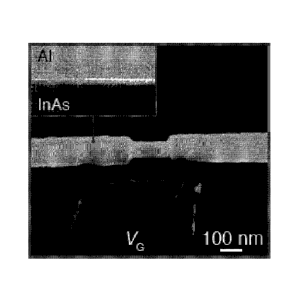
Fig. 1(A) shows a scanning electron micrograph of hybrid nanostructure in the
form of
an InAs-Al nanowire with a semiconductor weak link where the Al has been
removed
forming a Josephson junction. The weak link is formed by wet-etching a segment
(-180
nm) of the epitaxial Al shell. The inset shows a transmission electron
micrograph of the
epitaxial InAs/AI interface. The epitaxial interface between the
superconducting Al the
semiconductor InAs is leading to a proximity induced gap in the InAs core with
a low
density of states below the superconducting gap (a hard gap). The InAs
nanowire is
formed by MBE growth and is approximately 75 nm in diameter, with an in situ
grown
-30 nm thick Al shell.
Fig. 1(B-C) show optical micrographs of the completed tunable Josephson
junction
device according to the present disclosure. The total capacitance of the
tunable
Josephson junction, i.e. of the side gate controlled transmon qubit, CT, is
determined by
the capacitance of the T-shaped Al island to the surrounding Al ground plane.
The
center pin of the coupled transmission line cavity is indicated in Fig. 1(C).
The
coherence time is in the order of 1 s. The device as shown here is coupled to
a A/2
superconducting transmission line cavity with a bare resonance frequency
fc=5.96 GHz
and quality factor, Q-1500. Both the cavity and qubit leads are patterned by
wet
etching an Al film on an oxidized high resistivity Si substrate. The nanowire
contacts
and gate are also patterned from Al using a lift-off process with an ion mill
step to
remove the native A1203 prior to deposition.
Fig. 1(D) shows a schematic of the readout and control circuit. The cavity is
used for
dispersive readout of the qubit with homodyne detection. A supercurrent
leaking
through the semiconductor core links the un-etched regions and determines the
Josephson coupling energy, Ej(VG), which can be tuned by changing the electron
density in the semiconductor core with a nearby side gate voltage, VG.
Example 2 - strong coupling to a side gate controlled transmon qubit
Side gate controlled transmon cavity coupling is investigated by measuring
cavity
transmission at low drive power as a function of the cavity drive frequency
and gate
voltage, VG, with fo - fc (Fig. 2(A)). The solid blue line shows the bare
cavity resonance
CA 02953185 2016-12-21
WO 2016/000836 PCT/EP2015/054522
27
frequency, fc, while the solid green line indicates the gate-voltage dependent
qubit
frequency, fo(VG), extracted from the data.
Fig. 2(B) shows cavity transmission as a function of the cavity drive at the
position
indicated by the purple arrows in (A). Aperiodic fluctuations in the resonance
as a
function of VG, with regions of widely split transmission peaks, has been
observed (Fig.
2B). These gate-dependent, repeatable fluctuations in the cavity resonance are
associated with mesoscopic fluctuations in the nanowire transmission appearing
also
as fluctuations of normal-state conductance, GN(VG) which causes fluctuations
in the
side gate controlled transmon frequency. The changing qubit frequency, in
turn, pulls
on the cavity resonance, resulting in the observed response. The split cavity
peaks
indicate hybridized qubit and cavity states in the strong coupling regime. The
coupling
strength, g, is found to exceed the qubit and cavity decoherence rates,
allowing the
vacuum Rabi splitting to be resolved.
Fig. 20 shows frequency splitting between the hybridized qubit-cavity states
as a
function of fQ, as extracted from (A). From fitting to the data, it can be
extracted, that
g/21-r = 99 MHz.
Fig. 2D shows a parametric plot of the data from (A) as a function of the
cavity drive
and qubit frequency, fQ. The plot reveals the avoided crossing for the
hybridized qubit-
cavity states.
Example 3 - coherent control of a side gate controlled transmon qubit
Fig. 3(A) shows the qubit resonance frequency as a function of gate voltage,
VG, and is
observed as a distinct feature. Demonstrations of qubit control has been
performed in
the dispersive regime, fQ - fc g/21-r. fQ is obtained by measuring the qubit-
state
dependent cavity response following a second 2 us microwave tone. When the
qubit
drive was on resonance with fQ, a peak in the cavity response was observed,
yielding a
reproducible gate voltage dependence.
Fig. 4(B) shows coherent Rabi oscillations performed at point B in (A) (VG=
3.4 V) by
applying microwave pulse for time, T, to drive the qubit followed by a readout
microwave pulse to probe the cavity response. The main panel shows coherent
qubit
oscillations as a function of driving frequency and T. The lower panel shows
coherent
CA 02953185 2016-12-21
WO 2016/000836 PCT/EP2015/054522
28
oscillations at the qubit resonant frequency, corresponding to rotations about
the X-axis
of the Bloch sphere.
Fig. 4(0) shows coherent oscillations about the Z-axis of the Bloch sphere
performed at
point C in 3(A) (VG = 3.27 V) by applying a gate voltage pulse, AVG, to detune
the qubit
resonance frequency for time, T . A 15 ns microwave pulse is first applied to
rotate the
qubit into the X-Y plane of the Bloch sphere and, following the gate pulse, a
second
microwave pulse is used to rotate the qubit out of the X-Y plane for readout.
The main
panel shows coherent Z rotations as a function of AVG and T. The main panel
inset
shows the simulated qubit evolution based on fQ(VG) extracted from 3(A). The
lower
panel shows coherent Z oscillations as a function of T for AVG = 20.9 mV. In
both 4(B)
and 4(0) the demodulated cavity response, VH, is converted to a normalized
qubit state
probability by fitting X rotations to a damped sinusoid. The solid curves in
the lower
panels of 3(A) and 4(B) are also fits to exponentially damped sine functions.
The
observed precession frequency is consistent with the Lif 0 predicted from the
spectroscopy data in Fig. 3(A) (Fig. 4(0) main panel inset).
Example 4 - quantum coherence in a side gate controlled transmon qubit
Fig. 5(A) shows in the left panel a lifetime measurement for Sample 1 at point
B in Fig.
3A (VG = 3.4 V). A 30 ns pulse excites the qubit to the 11>-state and we vary
the wait
time, T, before readout. The solid line is a fit to an exponential curve. The
right panel
shows a Ramsey experiment used to determine T2* for Sample 1 with the wait
time, T,
between two slightly detuned 15 ns pulses varied before readout. The solid
curve is a
fit to an exponentially damped sinusoid.
If fig. 5(B) the lifetime and Ramsey experiments are repeated as in (A) for
Sample 2
with fo = 4.426 GHz (VG = -11.3 V). In red, is performed a Hahn echo
experiment by
inserting a pulse between two. The decay envelope is measured by varying the
phase,
cp, of the second 1T /2 microwave pulse and extracting the amplitude of the
oscillations.
The solid red line is a fit to an exponential curve
Example 5¨ Recipe for etching
Resist mask:
Prebake chip for 1 min at 1850
Spin A4 resist 4000rpm 45s
Bake for 4 min at 1850
CA 02953185 2016-12-21
WO 2016/000836
PCT/EP2015/054522
29
Ebeam exposure:
Define windows for etch. We used a 100keV ebeam system.
Dose 1200uC/cm2
Develop:
60s MIBK:IPA 1:3
10s IPA
Dry with nitrogen
02 plasma clean
Etch
12s Transene Aluminum Etchant type D at 500
30s DI water room temperature
10s IPA
dry with nitrogen
Remove resist mask in acetone
Example 6¨ Recipe for providing a contact and deposition of a gate
Resist mask:
Prebake chip for 1 min at 1850
Spin EL9 resist 4000rpm 45s
Bake for 1 min at 1850
Spin A4 resist 4000rpm 45s
Bake for 4 min at 1850
Ebeam exposure:
Dose 1200uC/cm2
Develop:
60s MIBK:IPA 1:3
10s IPA
Dry with nitrogen
02 plasma clean
CA 02953185 2016-12-21
WO 2016/000836
PCT/EP2015/054522
Metal deposition with ebeam evaporation system:
Argon ion milling to remove aluminum oxide
mm Ti
150nm Al
5
Lift off in acetone