Note: Descriptions are shown in the official language in which they were submitted.
CA 02953264 2016-12-21
WO 2016/001365 PCT/EP2015/065110
1
Nanoscale device comprising an elongated crystalline nanostructure
The present disclosure relates to nanoscale device comprising an elongated
crystalline
nanostructure, such as a nanowire crystal, a nanowhisker crystal or a nanorod
crystal,
and a method for producing thereof.
Background of invention
Electronic band gap engineering, doping, strain profiles and confinement in
crystalline
semiconductors, is a research field made possible by epitaxial growth of two-
dimensional heterostructure crystals. The ability to tailor and design the
electronic
environment has revolutionized semiconductor technology and has led to
breakthroughs in many areas, such as modern transistors, photovoltaics and
laser
technologies. Nanostructured crystals, such as nanowires, have drawn a lot of
attention
recently and recent advances in the epitaxial growth of nanostructured
crystals such as
nanowires, have opened new possibilities of tailoring the electronic
environment, which
has led to a wide variety of promising device applications, especially
electronic devices.
However, the performance of electronic devices based on nanostructured
crystals
depends on the quality of the interfaces between the different materials used.
Summary of invention
Semiconductor-metal interfaces play a key role in device applications ranging
from
quantum transport to photovoltaic devices. However, the performance of
nanowire
crystal based devices has been limited by the uncontrolled electronic
environment as a
result of the interfaces, which contains unbound states and possibly defects
and
impurities. A controlled electrical contacting of nanostructures would open
new paths
for designing high quality nanoscale devices. The present disclosure therefore
relates
to nanoscale device comprising an elongated crystalline nanostructure, such as
a
nanowire (crystal) or nanowhisker (crystal) or nanorod (crystal), having a
plurality of
substantially plane side facets and a first facet layer covering at least a
part of one or
more of said side facets, i.e. of at least part of the length of the elongated
crystalline
nanostructure,.
The presently disclosed nanoscale (or nanometer scale) device can be seen as a
hybrid and/or heterostructured nanoscale device with the elongated crystalline
nanostructure having a (at least a first) facet layer and may be referred to
as such in
this document.
CA 02953264 2016-12-21
WO 2016/001365 PCT/EP2015/065110
2
Core-shell semiconductor heterostructure (i.e. having layers of different
materials)
growth is known in the art and can be used as surface passivation, but the
semiconductor/metal (SE/M) interfaces has so far been uncontrolled on the
atomic
scale. The presently disclosed nanoscale devices where a first facet layer is
deposited
on the side facet(s) of an elongated crystalline nanostructure overcome this
problem
providing controlled electrical contacts of nanostructures. The nanoscale
devices have
been realized and exemplified by means of bottom-up growth of
semiconductor/metal
core-shell nanowire crystals by molecular beam epitaxy (MBE), preferably by
combination of vapour liquid solid (VLS) growth and MBE. One embodiment uses
InAs
for the nanowire crystal and Al is grown with epitaxially matched single plane
interfaces, which can be regarded as the ultimate limit of disorder free
contact.
In one embodiment of the invention each two-dimensional interface between a
side
facet of the elongated crystalline nanostructure and the first facet layer is
lattice
matched and/or domain matched in at least one dimension, possibly in both
dimensions. Naturally the elongated crystalline nanostructure may be provided
in a
semiconducting material, e.g. a semiconducting material selected from the
group of 111-
V combinations, such as InAs, InP, InSb, GaAs, GaSb, AlSb and InGaAs, or group
IV
elements such as Si or Ge, or 11-V1 combinations such as ZnO, ZnSe and CdSe,
or 1-VII
combinations. However, the elongated crystalline nanostructure may be provided
in a
metal or insulator material. The first facet layer may naturally be a metal
but may be
many types of materials. Further, the first facet layer may be provided in a
material with
superconducting properties below a critical temperature T.
A key aspect of the presently disclosed nanoscale device is that the elongated
nanostructure is crystalline, i.e. it is a single crystal or it is composed of
several
crystals, e.g. large single crystal elements, forming a crystalline structure.
In some
embodiments the elongated crystalline nanostructure may be seen as a
substantially
one-dimensional crystalline structure. The presently disclosed nanoscale
device has
been demonstrated in InAs with an Al facet layer with Wurtzite(WZ)/FCC or Zinc
Blende(ZB)/FCC crystal orientations, which can form uniform crystal
morphologies and
highly ordered and well defined epitaxial SE/M interfaces between the
semiconductor
(SE, e.g. InAs) and the metal (M, e.g. Al), which can be seen in Figs. 1 and
2.
However, the nanoscale device can be realized with other material combinations
with
similar structures and lattice spacings. For relevant FCC metals this could
for example
CA 02953264 2016-12-21
WO 2016/001365 PCT/EP2015/065110
3
be Au and Ag, and for semiconductors this is for example the other members of
the
'6.1 A family': GaSb and AlSb. Hence, high quality epitaxial growth of
contacts to
elongated crystalline nanostructures can therefore be realized with many
material
combinations.
As also demonstrated herein electrical devices have been provided using the
presently
disclosed nanoscale devices. They have been characterized at low temperature
confirming the high quality of the first facet layer (shell) and a barrier-
free contact
between the shell and the core due to the remarkable epitaxial match between
the InAs
nanowire core and the Al shell, both on single facets and multiple facets.
These
epitaxially matched interfaces can be regarded as the ultimate limit of metal
contacts to
semiconductors. The hybrid nanowires thus provide a conceptually new route
towards
nanowire electronics as it solves the general problem of forming electrical
nanowire/metal contacts.
Many present and future applications of superconductivity would benefit from
electrostatic gate control of carrier density which is a characteristic of
semiconductors.
Topological superconductivity can be realized with electrostatic gate control
of the
carrier density and this can provide a basis for topological quantum
information
processing. Hence, there has been tremendous interest in topologically non-
trivial solid
state matter. These materials have a number of unique properties, including
the
possibility to observe and manipulate Majorana bound states which have been
proposed as the basis for future fault tolerant quantum computation. A break-
through in
the search for Majorana fermions was the realization that under certain
conditions,
conventional superconductors can induce a topological non-trivial
superconducting
state in semiconductor nanowires. Proposals based on proximity effect in
semiconductor nanowires with strong spin-orbit are appealing because the key
ingredients are known in the art [8, 9]. However, all previous instances of
proximitized
semiconductors show significant tunneling conductance below the
superconducting
gap, suggesting a continuum of subgap states that nullifies topological
protection ¨ an
unsolved issue referred to as the "soft gap problem". Such soft-gaps will
induce
decoherence of Majorana qubits, and has been considered a major road-block for
the
future of topological quantum information in such devices. It turns out that
the hardness
of the induced superconductivity depends crucially on the quality and
uniformity of the
semiconductor/superconductor (SE/SU) interfaces. This situation is analogous
to that
of conventional semiconductor devices where the quality of the involved
interfaces is
CA 02953264 2016-12-21
WO 2016/001365 PCT/EP2015/065110
4
the primary parameter determining the performance. For this reason,
semiconductor
technology was revolutionized by the invention of epitaxial growth of
heterostructures,
which enables atomic-scale design of semiconductor interfaces and tailor-made
profiles of the electronic band structures, doping levels and strain. So far,
however, the
world of semiconductor epitaxy has had little to do with the world of
superconductivity.
But as demonstrated herein in example 3: for temperatures below the
superconducting
transition temperature aluminum becomes superconducting and the Al shell
induces a
superconducting gap into the InAs by virtue of the proximity effect. In
contrast to all
previous studies, however, the induced gap remains hard i.e., free of sub-gap
states,
likely due to the perfectly uniform InAsHAI interface. The presently disclosed
nanoscale
device therefore provides a solution to the soft-gap problem, because a hard
super-
conducting gap induced by proximity effect in a semiconductor, is demonstrated
by
using epitaxial Al-InAs superconductor-semiconductor hybrid nanowires. The
hard
induced gap, along with favorable material properties and gate-tunability,
makes the
presently disclosed nanoscale devices attractive for both conventional and
topological
superconducting qubits and other potential applications, as well as
fundamental studies
of mesoscopic superconductivity, and the presently disclosed hybrid structures
thereby
remove a main obstacle for using semiconductor nanowires as the backbone in
future
schemes of topological quantum information based on Majorana Fermions. In this
context it is noted that the InAsHAI epitaxial hybrids fulfill all basic
requirements
remaining for use in Majorana devices: strong spin-orbit coupling, large
critical parallel
magnetic field, and gate-tunability.
In one embodiment the nanostructure of the presently disclosed nanoscale
device is an
elongated hybrid nanostructure comprising a crystalline semiconductor
nanostructure
and wherein the first facet layer is a crystalline structured layer of a of
superconductor
material and wherein the crystalline structure of the semiconductor
nanostructure is
epitaxially matched with the crystalline structure of the first facet layer on
the interface
between the two crystalline structures. The epitaxial match between the
crystalline
structures of the semiconductor nanostructure and the first facet layer is
preferably
configured to induce a superconductor hard gap in the semiconductor
nanostructure,
i.e. by virtue of the superconducting properties and proximity of the first
facet layer, i.e.
at a temperature below the critical temperature of the superconductor material
of the
first facet layer. Preferably each two-dimensional interface between a plane
surface of
CA 02953264 2016-12-21
WO 2016/001365 PCT/EP2015/065110
the nanostructure and the first facet layer is domain matched and/or lattice
matched in
at least one dimension, or at least two dimensions.
Description of drawings
Fig. 1: Overview of an exemplary epitaxial InAsHAInanoscale device.
5 a. Tilt-view SEM image an array of InAs//A1 half-shell hybrid
structures grown on
an InAs (111)B substrate.
b. TEM image of the top part of a nanowire taken from the sample shown in a
with the Al shell covering to side facets to the right. The epitaxial Al layer
is -8nm
thick and covers two sidefacets of the nanowire as illustrated in the
schematic
cross section shown in the inset. The high resolution TEM image in panel
c. shows that the Al forms a perfectly sharp and uniform interface to the InAs
core. In this example, the InAs core was grown in the [0001]wz direction and
the
crystal orientation of the Al along the whole length of the nanowire is with
the
high symmetry and low energy (111) orientation normal to the interface.
Fig. 2. Domain matched InAsHAI interfaces. Three types of dominant epitaxial
bicrystal matches formed in three types on nanowire hybrid devices. The TEM
images
(a, d, f) are parallel views on the InAs//A1 interface along the transverse 1
direction,
where the atomic positions in the case of a perfect flat interface are
simulated in the
white boxes. The right column (b, c, e, g) show simulations of normal views on
the
interface. The red nets are primitive domains (assuming a perfect domain
match),
where the highlighted atoms specify one interfacial unit of each constituent
in the
parallel and transverse directions (shown with vectors).
Fig. 3. Aluminum shell morphology and asymmetric strain. TEM images of
different types of half-shell hybrid devices with varying shell thicknesses.
In a-c the
InAs core was grown along the [0001]wz direction, where a structural
transition from
{111} to {11-2} out of plane orientation is observed for critical thickness
beyond
20 nm . In d-e the InAs core was grown along the <1-100>wz direction and the
shell
remains uniform with {111} out of plane orientations. Scale-bars in a-e are 50
nm. f Tilt
view SEM close-up of a type-1 half-shell nanowire demonstrating the asymmetric
strain
induced by the Al on the InAs core, which causes nanowire to bend towards the
Al due
to the residual AlfilnAs interfacial domain mismatch, as discussed below.
CA 02953264 2016-12-21
WO 2016/001365 PCT/EP2015/065110
6
Fig. 4: Full shell epitaxial bicrystal match a) A TEM image of InAs nanowire
(seen as
the dark core) with a thick layer of epitaxial Al grown on all six {1-100}
facets, for which
the dominating out-of-plane grain orientation is of the {11-2} type. The two-
fold
degeneracy of the interface gives two variants a and p. These orientations
which are
seen by the TEM diffraction contrast in a, form a coherent twin along the
nanowire axis
as indicated in b and c. d is simulation of a full single crystal shell viewed
long the
nanowire axis, with alternating variants. If the same Al variants of the {11-
2} type
(indicated with m'=1) are formed on adjacent facets of the InAs nanowire, they
will form
an incoherent grain boundary when they merge, as in the case shown in e. which
is
because Al does not have 6-fold symmetry, as in the InAs host. However,
because a p
variant corresponds to a six-fold operation of a, they can merge and form a
single
crystal across adjacent facets. This means that the coherent interface shown
in Fig. 2b,
can be produced all around the InAs nanowire, where every second interface
differs by
only a screw axis translation indicated in the side view simulation in f.
Fig. 4g Growth of a AlAs barrier between InAs and Al. TEM micrograph of a 3nm
AlAs
high band-gap semiconductor layer separating the InAs core from the Al outer
shell.
The rightmost icon illustrates the type of nanowire device it is formed in.
Fig. 5 Electrical properties of the InAs/AI epitaxial hybrids.
a Illustration of a four-terminal device made from a full-shell InAs/AI
nanoscale
device with a 13nm Al full-shell.
b SEM image of the device. The scale bar is 0.5pm and the parallel orientation
of
the magnetic field is indicated.
c Measurements of the four-terminal resistance as a function of magnetic
field.
The nanoscale device is superconducting at low fields with Little-Parks peaks
appearing at half multiples of flux quanta threading the wire. Inset shows the
resistance as a function of temperature with a superconducting transition at -
1.4
Kelvin.
d Conductance as a function of gate-voltage for a device where the InAs core
has been exposed. Measurements are shows for various temperatures to
investigate the contact barriers between the core and the shell. Upper inset
shows a schematic of the sample, and the lower inset shows an SEM micrograph
of the central part of the actual device.
Fig. 6: Epitaxial full-shell nanoscale device and hard induced gap
CA 02953264 2016-12-21
WO 2016/001365 PCT/EP2015/065110
7
a, Cross-section schematic of an epitaxial full-shell nanowire.
b, Measurement set-up. Yellow represents normal metal (Au), green InAs, and
gray superconductor (Al).
c, TEM image of epitaxial N-S interface.
d, False colored SEM micrograph of a lithographically similar device.
e, Differential conductance as a function of source-drain voltage of an
epitaxial
full-shell device (blue) and an evaporated control device (red). Solid lines
represent data at zero magnetic field while dashed lines represent data at
fields
above the critical magnetic field, Bc.
f, Normalized differential conductance. Epitaxial full-shell nanowires exhibit
a
subgap conductance suppression of up to two orders of magnitude.
Fig. 7: Conductance of ballistic one-dimensional N-S junction in epitaxial
full-shell
device.
a, b, Differential conductance of a full-shell device as a function of
backgate,
VBG, and VSD.
c, Vertical cuts of a and b in the tunneling (orange), and open (blue)
regimes.
d Zero-bias versus finite-bias (0.4 mV) conductance. The solid line (red)
represents the theoretical relation between the two quantities.
e, Conductance steps as a function of VBG at zero-bias, above-gap bias, and
normal state (B = 100 mT> Bc).
Fig. 8: Epitaxial full-shell quantum point contact vs quantum dot devices.
a, Tunneling spectrum of a proximitized InAs core coupled to a QPC (upper
panel) and QD (lower panel).
b, Andreev bound states in a quantum dot. The green (orange) line indicates
the
particle-hole symmetry point of an even (odd) Coulomb diamond.
c, Vertical cuts of b.
d, Comparison of tunneling measurements between a QPC device and a QD
device in an even valley.
Fig. 9: Magnetic field and temperature dependence of induced gaps.
a, Magnetic field dependence of an epitaxial fullshell device.
b, Temperature dependence of an epitaxial full-shell device.
c, Comparison of normalized zero-bias conductance between the epitaxial device
and a control device as a function of normalized magnetic field.
CA 02953264 2016-12-21
WO 2016/001365 PCT/EP2015/065110
8
d, Comparison of normalized zero-bias conductance between the epitaxial device
and an evaporated control device as a function of temperature. Gray lines in c
and d are guides to the eye, and the blue line in d is a theoretical fit to
the data.
Fig. 10: Epitaxial half-shell device and gate-tunability of InAs core
a, Cross-section illustration of a half-shell nanowire.
b Gate-tunability measurement schematic of a half-shell nanowire device.
c, Comparison of induced gap quality between an epitaxial full-shell and half-
shell
device.
d, SEM micrograph of a lithographically similar device.
e, conductance of the Al shell and InAs core as a function of VBG.
Fig. 11 Main stages during epitaxial grain growth.
a,b An illustration of the initial stages of the metal growth evolution at
relatively
low and high temperatures.
In a, a low substrate temperature T1 gives small and closely spaced metal
grains
due to a relatively low adatom mobility, described by an average adatom
diffusion
length ilas,Em of species M on a facet of SE. The small grains will merge into
a
thin film, where if the film is thin enough, the grains with the lowest
surface
energy will grow on expense of the grain with higher surface energy (as
indicated
by the arrows).
In b, iias,Em is larger due to a higher temperature, T2 , which give larger
grains
separated further apart.
c, d Continuing growing, the both temperature regimes may evolve into new
preferred crystal orientations as the role of the grain boundaries and strain
contributions becomes increasingly important with increasing film thickness.
Fig. 12 Two-facet thin shell Al/InAs NWs.
a A SEM image of an array of InAs NWs with 10 nm of Al grown on two facets.
b A TEM image of a cross sectional cut through the NW array (in a region
similar
to the square blue region in a) which was cut out using a Ultra-Microtome
system.
Three examples of individual wires are shown in higher resolution and marked
with corresponding squared colour boxes. The Al is sitting to two facets,
which is
seen by the light grey contrast at the two top-right facets.
CA 02953264 2016-12-21
WO 2016/001365 PCT/EP2015/065110
9
c A TEM image of a single NW from the same growth as in a and b, where the
[111] out of plane orientation is seen all along the NW except where the
change
its diameter (green region). This is seen in the high resolution TEM images
indicated by the blue and red regions. In the red region both variants, a and
#
of the [111] out of plane orientation is shown (these are the only two
variants of
this type of interface according to equation (0)). In the green region the NW
surface is rough and the orientation of the Al phase gets mixed with no clear
orientation, indicated by the arrows pointing in various [111] directions.
Fig. 13: 'Thick' three-facet shell of Al grown on the InAs NW sidefacets.
a Topview cross sectional TEM image along the NW axis, where the dominating
faceting in the Al crystal follows the faceting of the InAs.
b Sideview TEM image, where the high resolution epitaxial match at the InAs/AI
interface is seen to follow the (11-2)//{1-100} coherent type. This
corresponds
well to the faceting seen in a, which suggests that the growth was terminated
in
the grain boundary driven growth mode according the to the discussion in Si
and
S2.
Fig. 14 Examples of symmetry diagrams of single plane bicrystals. The SE plane
symmetry is a fixed reference, while the M plane and bulk symmetry rotates
around a
point normal to the interface. If a given rotation gives the same plane
symmetry but
different bulk configuration, it is a variant, or specified in another way:
the number of
different M bulk orientations for a given interface pattern defines the number
of
degenerate variants, in this single plane symmetry limit.
Fig. 15 Illustrates the principle of depositing a second facet layer on to the
(first) facet
layer, in this case a layer of vanadium has been deposited onto a full shell
hybrid
nanoscale device with InAs/Al.
Fig. 16a Illustrates the schematic principle of an actual device with two
facet layers and
a gold contact.
Fig. 16b Shows a picture of an actual device with two facet layers and a gold
contact.
Fig. 17 Measurements of the gap properties of the device in fig. 16b.
CA 02953264 2016-12-21
WO 2016/001365 PCT/EP2015/065110
Detailed description of the invention
As stated previously the present disclosure relates to a nanoscale device
comprising
an elongated crystalline nanostructure, such as a nanowire (crystal) or
nanowhisker
(crystal) or nanorod (crystal), having a plurality of substantially plane side
facets and a
5 first facet layer covering at least a part of one or more of said side
facets. The terms
"nanowire" and "nanowire crystal" may be used interchangeably" herein, as it
may be
implicitly disclosed that the nanowires mentioned herein are crystalline
structures.
Naturally the first facet layer may crystalline. The two-dimensional interface
between a
10 side facet of the crystalline nanostructure and the first facet layer
may be epitaxial.
Even further the two-dimensional interfaces between each side facet of the
crystalline
nanostructure and the first facet layer may be epitaxial, such as
simultaneously
epitaxially matched. Thus, the crystalline structure of the nanostructure may
be
epitaxially matched with the crystalline structure of the first facet layer.
As also stated
previously each two-dimensional interface between a side facet of the
crystalline
nanostructure and the first facet layer may be domain matched and/or lattice
matched
in at least one dimension, preferably in both dimensions. Thus, in one
embodiment
each two-dimensional interface between the side facets of the crystalline
nanostructure
and the first facet layer is simultaneously epitaxially matched, domain
matched and
lattice matched in both dimensions.
Epitaxial match in the interface between two crystalline layers may not be
entirely
unusual if the crystal structures of the two crystalline layers are equal.
However, in this
case the inventors have demonstrated that an epitaxial interface can be
realised even
when the crystal structure (and/or crystal phase) of the elongated crystalline
nanostructure is different from the crystal structure (and/or crystal phase)
of the first
facet layer, such as when the crystal structure (and/or crystal phase) of the
elongated
crystalline nanostructure and the crystal structure (and/or crystal phase) of
the first
facet layer belong to different lattice systems and/or if the Bravais lattice
of the
elongated crystalline nanostructure is different from the Bravais lattice of
the first facet
layer. If for example the crystal structure of the elongated crystalline
nanostructure is
zincblende (ZB) then the crystal structure of the first facet layer is not
zincblende, i.e.
the crystal structures are different. Correspondingly if for example the
crystal structure
of the elongated crystalline nanostructure is wurtzite then the crystal
structure of the
first facet layer is not wurtzite, i.e. the crystal structures are different.
E.g. the crystal
structure of the elongated crystalline nanostructure may be zincblende (ZB) or
wurtzite
CA 02953264 2016-12-21
WO 2016/001365 PCT/EP2015/065110
11
(WZ) and the crystal structure of the first facet layer belongs to the cubic
crystal
system, such as primitive cubic, BCC or FCC, as demonstrated herein with InAs
nanowires (ZB or WZ) with an Al (FCC) epitaxially matched facet layer.
In further embodiment the first facet layer comprises one or more large single
crystal
segments wherein the interface between the elongated crystalline nanostructure
and
said single crystal segment(s) is epitaxially matched, such as simultaneously
epitaxially
matched on all side facets.
In one embodiment the elongated crystalline nanostructure is branched, e.g.
formed
from branched nanowhisker crystals. E.g. the elongated crystalline
nanostructure may
comprise one or more kinks.
The elongated crystalline nanostructure may be homogeneous, i.e. formed from
the
same compound material in the longitudinal! axial direction and/or in the
radial
direction. However, the elongated crystalline nanostructure may in itself be a
heterogeneous structure, e.g. a heterostructured nanowire crystal. E.g. the
crystalline
nanostructure may be a heterostructured nanowire crystal composed of different
compounds in the axial and/or radial direction.
As previously stated it is unusual that an epitaxial interface is provided
between layers
having different crystal structures and this opens for epitaxial interfaces
between
semiconductors (which are often wurtzite or zincblende) and metals (which are
often
BCC or FCC). In one embodiment the first facet layer is hence a metal selected
from
the group of Al, Ne, Ar, Ca, Ni, Cu, Kr, Sr, Rh, Pd, Ag, Xe, Ce, Yb, Ir, Pt,
Au, Pb, Ac,
Th, Li, Na, K, V, Cr, Fe, Rb, Nb, Mo, Cs, Ba, Eu, Ta and W. Some of these
metal
become superconducting below a critical temperatures. However, facet layers of
other
materials may as well be provided where an epitaxial interface to the
elongated
crystalline nanostructure can be realised, e.g. selected from the group of
high
temperature ceramic superconductors, such as copper oxide or cuprate
superconductors, which are often having a perovskite crystal structure.
The cross-section of the elongated crystalline nanostructure may e.g. be
square,
hexagonal, or octagonal providing a total of four, six or eight side facets,
respectively.
Consequently, the first facet layer may be covering at least a part of 1, 2,
3, 4, 5, 6, 7, 8
CA 02953264 2016-12-21
WO 2016/001365 PCT/EP2015/065110
12
or more of the side facets.
The thickness of the first facet layer may be less than 300 nm, or less than
250 nm, or
less than 200 nm, or less than 150 nm, or less than 100 nm, or less than 90
nm, or less
than 80 nm, or less than 70 nm, or less than 60 nm, or less than 50 nm, or
less than 45
nm, or less than 40 nm, or less than 35 nm, or less than 30 nm, or less than
25 nm, or
less than 20 nm, or less than 19 nm, or less than 18 nm, or less than 17 nm,
or less
than 16 nm, or less than 15 nm, or less than 14 nm, or less than 13 nm, or
less than 12
nm, or less than 11 nm, or less than 10 nm, or less than 9 nm, or less than 8
nm, or
less than 7 nm, or less than 6 nm, or less than 5 nm.
At the initial stage of the growth of the first facet layer islands may form
at the
elongated crystalline nanostructure surface. During this growth the
temperature of the
substrate may play an important role with regard to the spacing between the
islands. If
the temperature is low enough, the spacing is so small that the islands will
merge at a
very thin thickness of the first facet layer. As discussed further below this
may lead to
surface driven grain growth. A thickness of the first facet layer below 15 nm
may only
be obtained if the temperature during growth / deposition of the first facet
layer is below
-20 C, or below -25 C, or even below -30 C.
The diameter of the elongated crystalline nanostructure may be between 10 and
200
nm, such as between 10 and 20 nm, or between 20 and 30 nm, or between 30 and
40
nm, or between 40 and 50 nm, or between 50 and 60 nm, or between 60 and 70 nm,
or
between 70 and 80 nm, or between 80 and 90 nm, or between 90 and 100 nm, or
between 100 and 110 nm, or between 110 and 120 nm, or between 120 and 140 nm,
or between 140 and 160 nm, or between 160 and 180 nm, or between 180 and 200
nm.
The length of the elongated crystalline nanostructure may be between 1 and 20
um, or
between 1 and 2 um, or between 2 and 3 um, or between 3 and 4 um, or between 4
and 5 um, or between 5 and 6 um, or between 6 and 7 um, or between 7 and 8 um,
or
between 8 and 9 um, or between 9 and 10 um, or between 10 and 12 um, or
between
12 and 14 um, or between 14 and 16 um, or between 16 and 18 um, or between 18
and 20 um.
CA 02953264 2016-12-21
WO 2016/001365 PCT/EP2015/065110
13
Method
The present disclosure further relates to a method for producing a nanoscale
device.
Basically elongated crystalline nanostructures may be grown at elevated
temperatures,
e.g. above 300 C, above 350 C, or above 400 C, e.g. in the normal direction on
a
plane substrate. Importantly the first facet layer is grown / deposited
directly on at least
one side facet of the elongated crystalline nanostructures at a much reduced
temperature compared to what has previously been tried, e.g. below 50 C or
below
20 C. To provide a thin facet layer, e.g. on the order of 10 nm, the
temperature can be
reduced even further, i.e. below 0 C, or below -5 C, or below -10 C, or below -
15 C, or
below -20 C, or below -25 C, or most preferably below -30 C, during deposition
of the
first facet layer. The reduction in temperature may also help to prevent any
material
sticking at the nanowire surface before the first facet layer is deposited. An
oxide free
interface between the side facets and the first facet layer is thereby
obtained, i.e. an
oxide free epitaxial interface / contact between a semiconductor nanowire and
a metal
(or a superconductor) can be obtained, as demonstrated herein, where nanowires
grown in the conventional [0001]wz / [111]zB direction have a first facet
layer in the form
of a cubic metal phase with the [11-2] normal to the side facets of the
nanowire and
[111] along the nanowire axis. This is indeed unique because the symmetry
allows
large single crystal segments with simultaneous epitaxial match on all facets
of the
nanowire.
The inventors have realized that if the first facet layer is deposited at very
low
temperature it is possible to grow a first facet layer such that the two-
dimensional
interface between the first facet layer and the elongated crystalline
nanostructure is
epitaxially matched, even when the nanostructure and the first facet layer
have
fundamentally different crystal structures. This opens the door for epitaxial
matches
between semiconductors and metals on the side facets of nanostructures like
nanowires, as demonstrated herein. The key issue in the growth method is the
lgow
temperature when depositing the first facet layer to provide for initial
surface driven
growth of small crystal grains of the first facet layer. Thus, after the
elongated
nanostructures have been grown all sources (e.g. in an MBE chamber) must be
shut
off such that the growth chamber is empty and then lowering the temperature,
which
can be lowered to below 0 C or much lower, within seconds or minutes if
external
cooling sources like liquid nitrogen is used.
CA 02953264 2016-12-21
WO 2016/001365 PCT/EP2015/065110
14
The background pressure may also be reduced before the provision of the first
facet
layer. If the process takes place in a vacuum chamber, the background pressure
may
be reduced. This may also help to prevent any material sticking at the
nanowire surface
before the first facet layer is deposited. The presently disclosed method may
in one
embodiment be seen as a method for producing a metallic contact and/or
interface to a
semiconductor elongated crystalline nanostructure (e.g. a nanowire).
One embodiment relates to a method for producing a nanoscale device comprising
the
steps of:
a) growing, at an elevated temperature, such as above 400 C, one or more
elongated crystalline nanostructures in the normal direction on a plane
substrate,
b) reducing the temperature thereby cooling the substrate with the elongated
crystalline nanostructures to a temperature below 20 C, and
c) depositing, at said reduced temperature, a first facet layer directly on at
least
one side facet of the elongated crystalline nanostructures.
A further embodiment relates to method for producing a nanoscale device in a
vacuum
chamber by means of molecular beam epitaxy (MBE), the method comprising the
steps
of
a) growing, e.g. by means of vapour liquid solid (VLS) growth, at an elevated
temperature of above 400 C, one or more elongated crystalline nanostructures,
such as nanowire (crystals), in the normal direction on a plane substrate,
b) shutting off all sources of growth material and reducing the temperature
thereby
cooling the substrate with the crystalline nanostructures to a temperature
below
-30 C, and
c) depositing, at said reduced temperature, a crystalline first facet layer
directly on
at least one side facet of the crystalline nanostructures.
The method may be provided for production of the presently disclosed nanoscale
device. The step of growing in the methods disclosed herein may therefore
comprise
growing the elongated crystalline nanostructure of the presently disclosed
nanoscale
device. Similarly the step of depositing may be the deposition of the first
facet layer of
the presently disclosed nanoscale device. The presently disclosed methods may
furthermore comprise one or more steps of depositing the second and/or third
facet
layers as disclosed herein.
CA 02953264 2016-12-21
WO 2016/001365 PCT/EP2015/065110
The method may be provided by means of MBE and growth may be provided by the
vapour liquid solid growth method. Hence, the plane substrate may be located
in ultra-
high vacuum in a vacuum chamber, e.g. MBE chamber, and may be prepared with
5 catalysing particles, such as Au particles, which is a normal growth
method of
elongated crystalline nanostructures.
In order to hit the side facet(s) of the elongated crystalline nanostructures
when
growing the first facet layer, the source of the first facet layer may be
located at a finite
10 angle, e.g. less than 10 deg or less than 5 deg, such as 2-3 degrees,
(e.g. inside an
MBE vacuum chamber) to the normal direction of the substrate during deposition
of the
first facet layer. In order to cover additional side facets of the elongated
crystalline
nanostructures the substrate may be rotated during deposition of the first
facet layer.
15 As also stated previously the temperature of the substrate before
deposition of the first
facet layer may preferably be reduced to a temperature below 10 C, or below 0
C, or
below -5 C, or below -10 C or below -15 C, or below -20 C, such as below -25
C,
more preferably below -30 C. These low temperatures have been realized in a
standard MBE chamber by reducing the background pressure and waiting for
several
hours. However, the temperature may be reduced much faster by applying an
external
source of cooling, e.g. liquid nitrogen, to cool the substrate. Even lower
temperatures
for depositing / growing the first facet layer can then be reached. However,
most
importantly the time to reach the low temperatures can be much reduced.
The nanowire is typically at least initially grown in the vertical direction
normal to the
substrate. However, the growth direction of the elongated crystalline
nanostructure can
be kinked during growth. The growth direction may for example be kinked by
means of
a short flush of Ga25 or by means of a short temperature drop during growing
of the
elongated crystalline nanostructure.
As an example InAs nanowires were grown in two different crystal directions on
(111)B
InAs substrates by the Au-catalyzed vapor-liquid-solid method in a solid-
source Varian
GEN-II MBE system. The first type is the conventional nanowires with an axial
(0001)B
wurtzite (WZ) orientation growing vertical on the substrate, with a
corresponding planar
growth rate of 0.5 m/hr and a V/III ratio of -100 for 30 minutes at a
substrate
temperature of 420 C. These conditions provide a pure WZ crystal structure
with flat
CA 02953264 2016-12-21
WO 2016/001365 PCT/EP2015/065110
16
side facets. The second type is grown perpendicular to the substrate, after
kinking the
growth direction of the conventional nanowires into one of the six equivalent
<1-100>
orientations, which was obtained by either a short flush of Gal or a short
temperature
drop and back up again. Hereafter the substrate is cooled below -30 C, by
turning of all
power sources which can act as heat sources. This process may take more than 8
hours in a chamber without cooling sources. For the half shell growth the
substrate
rotation is disabled and the substrate is visually oriented with an accuracy
of -2-3
degrees to have the desired crystal orientation facing the Al cell. RHEED can
be used
as an alternative for substrate alignment.
The thickness of the metal phase on the nanowire facets is given by,
s(t)= x S2s sin (v) f = i , where Q.s is the atomic volume, co is the angle of
the incoming
beam with respect to the facet normal, f the incoming flux of growth species,
and x is
a correction factor for the time the beam is effectively hitting the facets.
The
corresponding planar growth rate (S2sf cos(v) ) for the Al growth was 0.3-0.5
m/hr.
After growth the substrate can be turned away from the sources and put at room
temperature in the buffer chamber, before any heat sources (power supply for
substrate holder, ion gauges, light sources) are turned on in the growth
chamber.
Morphological evolution during epitaxial growth of a NW metal shell
The surface kinetics of adatoms seems to play a role in the complicated
evolution of
the crystal morphology when the first facet layer is grown of the side facets.
A low
substrate temperature during deposition of the first facet layer promotes
formation of
small and closely spaced islands because the adatom mobility at the
nanostructure
surface may be small (Fig. 11a). As the islands grow bigger, they will merge
into a thin
film, and if the film is thin enough when the islands merge, minimization of
surface
energy dictates the out-of-plane grain orientation. E.g. for most FFC metals,
this will
lead to flat and uniform (111) low energy surfaces (as shown for InAs/A1 in
Fig. 12). A
higher temperature will increase the adatom mobility, which results in islands
spaced
further apart, as illustrated in fig. 11b. When larger islands merge, the film
may have
exceeded a certain thickness where the role of primarily in-coherent grain
boundaries
and strain fields becomes the dominating driving forces for grain growth, and
the
growth may never pass through the surface driven stage. At the later stages in
growth
CA 02953264 2016-12-21
WO 2016/001365 PCT/EP2015/065110
17
(as illustrated in fig. 11 c, d), for both relative low and high temperatures,
there can be
nucleation of new preferential orientations and reconstruction of the metal
phase.
Epitaxial interfaces - interfacial bicrystal symmetries and degenerate grain
orientations
Crystalline materials with different crystal structures (e.g. many
combinations of
semiconductors and metals) are in general incommensurate in their relaxed
states, but
when put together they can have preferred relative orientations, which depend
on the
lattice constants and symmetries of the constituents. It is not only the
interface
energies that determine relative orientations but also surface and grain
boundaries play
an important role. Based on TEM measurements on many different types of
InAs/AI
NWs, it is for example clear that there exist a preferential out-of-plane
orientation of the
Al phase, for a given phase thickness and type of core-shell hybrid structure.
Moreover,
for each out-of-plane orientation there seems to be a very limited number of
in-plane
orientations present. The principle of epitaxial rotation of unstrained
structures has
previously been formulated; however, the results presented herein suggest that
the
interfaces try to minimize the energy by forming small domains. Thus, the in-
plane high
symmetry bicrystal rotations of a given out-of-plane orientation may be
analysed. It
turns out that orientations that differ in the bulk can have, if not
identical, then almost
identical interfaces, and they will therefore be regarded as degenerate (for
the growth
analysis). The bilayer rotational symmetries normal to the interface of two
joining
arbitrary crystals can be analyzed, e.g. a semiconductor SE and a metal M,
where SE
is considered as a fixed reference. For a given out of plane orientation of M,
there exist
a given number of degenerate crystal orientations, i.e. with indistinguishable
interfacial
planes, but with distinguishable crystal orientations in M. We will call the
crystal
orientations that correspond to a given type of SE/M interface for the
variants of M.
The epitaxial relation and ordering of the SE/M interfaces is described in
terms of
domain matching. That is, when a lattice mismatch of a given SE/M material
combination is large, interfacial domains - consisting of nm and n sE
interfacial units of
M and SE- form, in order to reduce the stress associated with the mismatch. We
will
describe a given SE/M interface with the interfacial domain notation:
( (
nm, nm,
¨, e x ¨, e _L , where ¨nm denotes the ratio of domain units in two orthogonal
nSE
y
SE
, \nSE,1 y
directions in the interfacial plane, parallel and transverse 1 to the NW axis.
e is the
corresponding residual mismatch in the respective directions as expected from
relaxed
structures at room temperature.
CA 02953264 2016-12-21
WO 2016/001365 PCT/EP2015/065110
18
For a given out of plane orientation of M, there exists a set of variants with
certain in-
plane orientations that minimizes the free energy. From the set of variants,
the low
energy grain boundaries can be obtained. Based on these statements, a simple
general framework is provided to describe the structure of M, in terms of
symmetries of
M and SE. For NWs with rough surfaces, the orientation of the grains becomes
more
random, see Fig. 1 c. We are here only interested in the planar SE surfaces,
and we
neglect for simplicity what we assume to be small energy differences arising
from
polarity in the SE. The order of the plane rotational symmetries (PRS) of SE
and M
along a given crystal axis i will be denoted, CiPsT-L and Cr", respectively.
The
superscript 1 specifies that we are considering the symmetries in the
transverse
direction, i.e. a single interface. Note that the PRS is not necessarily the
same as the
order of the corresponding symmetry operation CE and Ci-Lx of the bulk
crystallographic point groups, as an atomic plane can have higher symmetry
than the
corresponding bulk operation. Thus, for a single SE/M interface i, the number
of
distinguishable degenerate crystal orientations in Mare given as
cr,sREs cr,AIRS ,1)
= ____________________________________ (0)
Ctlx
where (CiPs7,C,T ) is the least common multiple of CiPsREs and CiP: . Equation
(0)
can be visualized using the bicrystal symmetry diagrams presented in Fig. 14.
We now consider symmetries along the NW axisõ and restricting the single
facets to
have only one class of variants. We will also assume that the cross sectional
crystal
shape of the NW follows the Wulff shape containing only the highest symmetry
facets.
Then we can say that if CsE = Cm there can be mil ¨1 different types of grain
boundaries across the facets. If these grain boundaries are incoherent, they
induce a
high driving force for grain growth to eliminate the boundary across the
facets, where
the grain growth does not introduce new classes of variants due to the
bicrystal
symmetries. More general, if a given variant of the transverse dimension falls
into
symmetry operations of the parallel dimension, it will not contribute to new
class of
variants.
CA 02953264 2016-12-21
WO 2016/001365 PCT/EP2015/065110
19
Epitaxial domain matching for other material combinations
It may be difficult to predict material combinations which will form epitaxial
interfaces
SE/M NW heterostructures with a good epitaxial match. For example, surface
diffusion
lengths of metals on semiconductors are not generally available in the
literature, and
for a given metal, the large number of possible planes and surface
orientations makes
it difficult to predict domain matches. However, in the thick shell limit,
where strain and
grain boundary driven growth dominates, the lowest energy configuration is
most likely
when the SE and M crystals with similar symmetry groups (ZB or WZ and FCC)
orientate along the same type of symmetry classes, especially if the bicrystal
match is
not to large. For nanowires grown in the conventional [0001]wz / [111]zB
direction, a
cubic metal phase with the [11-2] normal to the facets and [111] along the
nanowire
axis is unique in that its symmetry allow large single crystal segments with
simultaneous epitaxial match on all facets of the nanowire. Thus, it is
natural to expect,
that if this orientation matches the semiconductor for a particular metal, it
is likely to
form in the thick film limit. Thus it is interesting to search among the cubic
metals for
matches in this orientation. Table 1, 2 and 3 list the domain strains for a
range of
metals grown on the important cases of InAs, InSb, and GaAs. In the general
notation
( n (
m
nM 1
=,e x =,e_L , we distinguish between interfacial match of interfacial units in
nSE, y \nSE,1 y
the components and the corresponding strain along the length and along the
transverse direction to the NW, as expected from relaxed bulk values.
If ZB and FCC orientation along the same type symmetry classes, the two
numbers are
identical in the parallel and perpendicular directions. The tables below are
suggestions
for possible feasible material combinations ¨ combinations without match in
the tables
may form epitaxial interfaces in other orientations.
CA 02953264 2016-12-21
WO 2016/001365
PCT/EP2015/065110
Domain fraction
ZB//FCC 1/2 1/3
2/3 1/4 3/4 1/5 2/5 3/5 4/5
FCC Lattice
metal const.
Ne 4.43 31.6 54.4 8.8 65.8' 6 72.6 45.3
17.9 9.4
Al 4.05 25.2 50.1 -) 62.6
12.2 70.1 40.2 10.2 19.7
Ar 5.26
42.4 61.6 23.2 71.2 13.6 77.0 53.9 30.9 7.9
Ca 5.58
45.7 63.8 27.6 72.9 18.6 78.3 56.6 34.9 13.1
Ni 3.52 13.9 42.6 14.7 57.0 29.1 65.6 31.2 37.7
Cu 3.61 16.1 44.1 11.9 58.0 25.9 66.4
32.9 0.7 34.3
Kr 5.72
47.0 64.7 29.4 73.5 20.6 78.8 57.6 36.5 15.3
Sr 6.08
50.2 66.8 33.6 75.1 25.3 80.1 60.1 40.2 20.3
Rh 3.8 20.3 46.9 6.3 60.1 19.6 68.1
36.2 -.3 27.5
Pd 3.89 22.1 48.1 3,8 61.1 16.8 68.9
37.7 6.6 24.6
Ag 4.09 25.9 50.6 13 63.0
11.1 70.4 40.8 11.1 18.5
Xe 6.2 51.1
67.4 34.9 75.6 26.7 80.5 60.9 41.4 21.8
Ce 5.16
41.3 60.9 21.7 70.6 11.9 76.5 53.0 29.6 6.1
Yb 5.49
44.8 63.2 26.4 72.4 17.2 77.9 55.9 33.8 11.7
Ir 3.84 21.1 47.4 5.2 60.6 18.3 68.4
36.9 5.3 26.2
Pt 3.92 22.7 48.5 ' 0 61.4 15.9 69.1 38.2
7.3 23.6
Au 4.08 25.8 50.5 1.0 62.9
11.4 70.3 40.6 10.9 18.8
Pb 4.95
38.8 59.2 18.4 69.4 8.2 75.5 51.0 26.6 2.1
Ac 5.31
43.0 62.0 23.9 71.5 14.4 77.2 54.4 31.5 8.7
Th 5.08
40.4 60.2 20.5 70.2 10.6 76.1 52.3 28.4 4.6
ZB//BCC
Li 3.49 13.2 42.1 15.7 56.6 30.2 65.3
30.6 4.2 38.9
Na 4.23 28.4 52.3 4.5 64.2
7.4 71.4 42.7 14.1 14.6
5.23 42.1 61.4 22.8 71.0 13.1 76.8 53.7 30.5 7.3
V 3.02 0.3 33.1 33.7
49.8 50.5 59.9 19.8 20.4 60.5
Cr 2.88 5.2
29.9 40.2 47.4 57.8 57.9 15.9 26.2 68.3
Fe 2.87 5.5
29.6 40.7 47.2 58.3 57.8 15.6 26.7 68.9
Rb 5.59
45.8 63.9 27.7 72.9 18.7 78.3 56.6 35.0 13.3
Nb 3.3 8.2 38.8
22.4 54.1 37.7 63.3 26.6 10.2 46.9
Mo 3.15 3.8
35.9 28.2 51.9 44.2 61.5 23.1 15.4 53.9
Cs 6.05
49.9 66.6 33.2 75.0 24.9 80.0 59.9 39.9 19.9
Ba 5.02
39.7 59.8 19.5 69.8 9.5 75.9 51.7 27.6 3.5
Eu 4.61
34.3 56.2 12.4 67.1 1,4 73.7 47.4 21.2 5.1
Ta 3.31 8.5 39.0 22.0 54.2
37.3 63.4 26.8 9.8 46.4
3.16 4.1 36.1 27.8
52.1 43.8 61.7 23.3 15.0 53.4
Table 1. Domain matching for InAs with different cubic metals in the [11-2]
out-of-plane
orientation.
CA 02953264 2016-12-21
WO 2016/001365
PCT/EP2015/065110
21
Domain fraction 1/2 1/3 2/3 1/4 3/4 1/5 2/5
3/5 4/5
fcc lattice
metal const
Ne 4.43 26.9 51.2 63.4 9.7
70.7 41.5 12.2 17.0
Al 4.05 20.0 46.7 6.7 60.0 20.0 68.0 36.0 /- 28.0
Ar 5.26
38.4 58.9 17.9 69.2 7.6 75.4 50.7 26.1 1
Ca 5.58
41.9 61.3 22.6 71.0 12.9 76.8 53.6 30.3 7.1
Ni 3.52 8.0 38.6
22.7 54.0 38.0 63.2 26.4 10.4 47.3
Cu 3.61 10.3 40.2 19.6
55.1 34.6 64.1 28.2 7.7 43.6
Kr 5.72
43.4 62.2 24.5 71.7 15.0 77.3 54.7 32.0 9.4
Sr 6.08
46.7 64.5 29.0 73.4 20.1 78.7 57.4 36.1 14.8
Rh 3.8 14.8 43.2 13.7
57.4 27.9 65.9 31.8 2..3 36.4
Pd 3.89 16.7 44.5 11.0 58.4 24.9 66.7 33.4 0.1 33.2
Ag 4.09 20.8 47.2 5.6 60.4 18.8 68.3
36.6 5.0 26.7
Xe 6.2 47.8
65.2 30.3 73.9 21.6 79.1 58.2 37.3 16.4
Ce 5.16
37.2 58.1 16.3 68.6 5.8 74.9 49.8 24.7 ft/1
Yb 5.49
41.0 60.7 21.3 70.5 11.5 76.4 52.8 29.2 5.6
I r 3.84 15.6 43.8 12.5 57.8 26.5 66.3
32.5 1.2 35.0
Pt 3.92 17.4 44.9 10.2 58.7 24.0 66.9 33.9 0.8 32.2
Au 4.08 20.6 47.1 5.9 60.3 19.1 68.2
36.5 4.7 27.0
Pb 4.95
34.6 56.4 12.7 67.3 1.8 73.8 47.6 21.5 47
Ac 5.31 39.0 59.3 18.7 69.5 8.5 75.6 51.2 26.8
Th 5.08 36.2 57.5 15.0 68.1 4.3 74.5 49.0 23.5
BCC
Li 3.49 7.2 38.1
23.8 53.6 39.2 62.9 25.7 11.4 48.5
Na 4.23 23.4 48.9 2.1 61.7 14.9 69.4
38.7 8.1 22.5
5.23 38.1 58.7 17.4 69.0 7.1 75.2 50.4 25.7 0.9
V 3.02 7.3 28.5
43.0 46.4 60.9 57.1 14.2 28.7 71.6
Cr 2.88
12.5 25.0 50.0 43.8 68.7 55.0 10.0 35.0 80.0
Fe 2.87 12.9 24.8 50.5 43.6 69.3 54.9 9.7 35.4
80.6
Rb 5.59
42.0 61.4 22.7 71.0 13.1 76.8 53.6 30.5 7.3
Nb 3.3 3 34.6
30.9 50.9 47.3 60.7 21.5 17.8 57.1
Mo 3.15 3 31.4
37.1 48.6 54.3 58.9 17.7 23.4 64.5
Cs 6.05
46.5 64.3 28.6 73.2 19.7 78.6 57.2 35.7 14.3
Ba 5.02
35.5 57.0 14.0 67.7 3.2 74.2 48.4 22.6 3.3
Eu 4.61 29.7 53.2 6.3 64.9
5.4 71.9 43.8 15.7 12.4
Ta 3.31 2.. 34.8
30.5 51.1 46.8 60.9 21.7 17.4 56.6
3.16 2. 31.7
36.7 48.7 53.8 59.0 18.0 23.0 64.0
Table 2 Domain matching for InSb with different cubic metals in the [11-2] out-
of-plane
orientation.
CA 02953264 2016-12-21
WO 2016/001365 PCT/EP2015/065110
22
Domain fraction 1/2 1/3 2/3 1/4 3/4 1/5 2/5
3/5 4/5
fcc lattice
metal const
Ne 4.43 36.2 57.5 14.9 68.1 4.3 74.5
49.0 23.4 2.1
Al 4.05 30.2 53.5 6.9 65.1 4.7
72.1 44.2 16.2 11.7
Ar 5.26 46.3
64.2 28.3 73.1 19.4 78.5 57.0 35.5 14.0
Ca 5.58 49.3
66.2 32.5 74.7 24.0 79.7 59.5 39.2 18.9
Ni 3.52 19.7 46.5 7.1 59.8 20.5 67.9 35.8 3.6 28.5
Cu 3.61 21.7 47.8 4.4 60.9 17.4 68.7 37.4 6.0 25.3
Kr 5.72
50.6 67.1 34.1 75.3 25.9 80.2 60.5 40.7 20.9
Sr 6.08 53.5
69.0 38.0 76.8 30.3 81.4 62.8 44.2 25.6
Rh 3.8 25.6
50.4 0.8 62.8 11.6 70.2 40.5 10.7 19.0
Pd 3.89 27.3 51.6 3.1 63.7 9.0 70.9
41.9 12.8 16.3
Ag 4.09 30.9 53.9 7.9 65.4 3.7 72.4
44.7 17.1 10.6
Xe 6.2
54.4 69.6 39.2 77.2 31.6 81.8 63.5 45.3 27.1
Ce 5.16
45.2 63.5 27.0 72.6 17.8 78.1 56.2 34.3 12.4
Yb 5.49 48.5
65.7 31.4 74.3 22.8 79.4 58.8 38.2 17.6
Ir 3.84 26.4 50.9 3 63.2 10.4
70.6 41.1 11.7 17.8
Pt 3.92 27.9 51.9 63.9 8.2 71.2
42.3 13.5 15.4
Au 4.08 30.7 53.8 7.6 65.4 3.9 72.3
44.6 16.9 10.8
Pb 4.95 42.9
61.9 23.9 71.4 14.3 77.2 54.3 31.5 8.6
Ac 5.31 46.8
64.5 29.0 73.4 20.2 78.7 57.4 36.1 14.8
Th 5.08 44.4
62.9 25.8 72.2 16.5 77.7 55.5 33.2 11.0
BCC
Li 3.49 19.0 46.0 8.0 59.5 21.5 67.6 35.2 2.8 29.6
Na 4.23 33.2 55.5 10.9 66.6 0.2 73.3
46.5 19.8 6.9
5.23 46.0 64.0 27.9 73.0 18.9 78.4 56.8 35.1 13.5
V 3.02 6.4
37.6 24.8 53.2 40.4 62.6 25.1 12.3 49.8
Cr 2.88 1.9
34.6 30.9 50.9 47.2 60.7 21.5 17.8 57.0
Fe 2.87 1.5
34.3 31.3 50.8 47.7 60.6 21.2 18.2 57.6
Rb 5.59 49.4
66.3 32.6 74.7 24.2 79.8 59.5 39.3 19.1
Nb 3.3 14.3 42.9
14.2 57.2 28.5 65.7 31.5 2.8 37.0
Mo 3.15
10.3 40.2 19.6 55.1 34.6 64.1 28.2 7.7 43.6
Cs 6.05
53.3 68.9 37.7 76.6 29.9 81.3 62.6 43.9 25.2
Ba 5.02 43.7
62.5 24.9 71.8 15.5 77.5 55.0 32.4 9.9
Eu 4.61 38.7 59.1 18.2 69.3 8.0 75.5
50.9 26.4 .9
Ta 3.31 14.6 43.1 13.9 57.3 28.1 65.8 31.7 2.E 36.6
3.16 10.5 40.4 19.3 55.3 34.2 64.2 28.4 7.3 43.1
Table 3: Domain matches for GaAs with different cubic metals in the [11-2] out-
of-plane
orientation.
Fabrication of electrical devices
The InAs/A1 hybrid devices were liberated from their growth substrate by a
brief
sonication in methanol, and a small amount of the resulting suspension was
deposited
on doped Si substrates capped with 500nm Si02. Wires were located with respect
to
predefined alignment marks using optical dark field microscopy and the ends of
the
wires were contacted using electron beam lithography (6% copolymer, 4% poly-
[methyl
methacrylate] (PMMA)) and electron beam evaporation of -5/100 nm of Ni/Au or
Ti/Au
(AJA International, ATC ORION evaporator). The oxide on the Al surface was
removed
CA 02953264 2016-12-21
WO 2016/001365 PCT/EP2015/065110
23
by 120 sec of Kaufmann argon ion milling performed inside the metal
evaporation
chamber (300 Volts acceleration, 46mA emission current). This procedure
reproducibly
created contact to the Al shell.
For the devices with exposed InAs cores, narrow etch windows were defined in
4%
PMMA resist by e-beam lithography, and the shell was removed by a -2 sec etch
in
12% hydrofluoric acid. Finally, the device is coated in 20-30nm of hafnium
oxide using
atomic layer deposition. Note, that in order to employ the Al shell to aid
electrical
contacts, the second lithography step is in principle obsolete as the first
metal layer can
act as the etch mask for exposing the InAs core. Low temperature electrical
measurements were performed in a dilution refrigerator (Leiden Cryogenics or
Oxford
Triton) using Stanford 5R830 lock-ins with a 100 ac excitation.
Applications
Further aspects of the present disclosure relate to various application of the
nanoscale
device, e.g. a quantum point contact comprising a nanoscale device as herein
disclosed having a semiconducting core and a superconducting facet layer. A
further
application is a superconducting field effect transistor comprising one or
more of the
presently disclosed nanoscale devices and/or electrical devices / contacts.
Second facet layer
As stated previously the present disclosure relates to a nanoscale device
comprising
an elongated crystalline nanostructure, such as a nanowire (crystal) or
nanowhisker
(crystal) or nanorod (crystal), having a plurality of substantially plane side
facets and a
first facet layer, i.e. a first facet layer, covering at least a part of one
or more of said
side facets. As demonstrated herein in example 3 in the case of a InAs
nanowire with
aluminum forming the first facet layer: for temperatures below the
superconducting
transition temperature aluminum becomes superconducting and the Al shell
induces a
superconducting gap into the InAs by virtue of the proximity effect. In
contrast to all
previous studies, however, the induced gap remains hard i.e., free of sub-gap
states,
likely due to the perfectly uniform InAs//A1 interface. Aluminum is just one
example of a
superconductor and as listed herein there are other possible candidates for
epitaxial
matching of semiconductors and superconductors.
Other superconductors have different advantageous properties, such as higher
critical
temperatures and in particular higher critical magnetic fields, than those
offered by
CA 02953264 2016-12-21
WO 2016/001365 PCT/EP2015/065110
24
aluminum. As a superconductor aluminum has a critical transition temperature
Tc of
approx. 1.3 Kelvin and a low critical magnetic field Bc. For many applications
other
superconductors with higher Tc and Bc are desired. For example, niobium has a
Tc of
-9 Kelvin and vanadium Tc of -5 Kelvin; using these elements as
superconductors
would therefore enable superconducting devices operating above liquid helium
temperature (4 Kelvin) making them much more attractive for various
superconducting
applications. Also, niobium and vanadium has high Bc enabling the operation of
superconducting devices in the presence of a sizable (order Tesla) field scale
as
needed for e.g., topological quantum information with Majorana Fermion bound
states.
Other superconductors and alloys have even higher Tc and Bc.
However, it can be difficult to find a semiconductor material where an
epitaxial match
with these other types of superconductors is obtainable. Another ingenious
option may
then be to use the first facet layer, e.g. in the form of epitaxially matched
aluminum, as
a coupling layer for interfacing a second - and different - facet layer to the
nanoscale
device, e.g. a second facet layer in the form of another type of material,
alloy, or metal
that become superconducting below T. In a further embodiment the presently
disclosed nanoscale device may therefore comprise a second facet layer located
on
the outside or covering at least a part of the first facet layer, the second
facet layer
being different than the first facet layer. Fig. 15 illustrates the principle
of depositing a
second facet layer directly on to the first facet layer, in this case a layer
of vanadium
has been deposited onto a full shell hybrid with InAs/Al.
The first facet layer may have a crystalline structure which is epitaxially
matched with
the crystalline structure of the nanostructure. In this case the structure of
the second
facet layer is not necessarily important, i.e. second facet layer may have a
crystalline
structure which is or is not epitaxially matched with the crystalline
structure of the
nanostructure. The second facet layer may even have an amorphous structure.
The crystalline nanostructure may be provided in a semiconducting material,
the first
facet layer may be provided in a first material with superconducting
properties below a
first critical temperature, and the second facet layer may be provided in a
second
material with superconducting properties below a second critical temperature.
The thickness of the first facet layer is preferably less than 20 nm, more
preferably less
than 10 nm, even more preferred less than 8 nm, and more preferred less than 6
nm,
CA 02953264 2016-12-21
WO 2016/001365 PCT/EP2015/065110
and most preferred less than 5 nm.
The thickness of the second facet layer is preferably at least 50 nm, or
greater than
100 nm, or greater than 150 nm, or greater than 200 nm, or greater than 300
nm. The
5 thickness of the second facet layer is preferably at least two times the
thickness of the
first facet layer, or at least 3, 4, 5, 6, 7, 8, 9 or at least 10 times the
thickness of the first
facet layer.
The first facet layer may be a metal selected from the group of Al, Ca, Ni,
Cu, Kr, Sr,
10 Rh, Pd, Ag, Ce, Yb, Ir, Pt, Au, Pb, Ac, Th, Li, Na, K, V, Cr, Fe, Rb,
Nb, Mo, Cs, Ba, Eu,
Ta and W, whereas the second facet layer may be a metal, different from the
first facet
layer and, and selected from the group of Al, Ca, Ni, Cu, Kr, Sr, Rh, Pd, Ag,
Ce, Yb, Ir,
Pt, Au, Pb, Ac, Th, Li, Na, K, V, Cr, Fe, Rb, Nb, Mo, Cs, Ba, Eu, Ta and W.
15 The material of the second facet layer may be selected among a list of
materials that
becomes superconducting below a critical temperature and such lists are known
in the
art, e.g. it may be selected from the group of superconducting ceramic
materials, in
particular cuprates such as YBCO (YBa2Cu307,) or superconducting alloys. There
are
many types of superconducting alloys known in the art and which can be
employed
20 here, such as Mg B2, niobium alloys such as NiTi and NbTiN with various
fractions of Ti
and N, and Zr100Mx where x is any number in the range of 0 to 100 and M is a
metal
selected from the group of Fe, Co, Ni, Cu, Ru, Rh, Pd, Os, Ir, Pt and Au.
The crystalline nanostructure is preferably provided in a semiconducting
material, such
25 as selected from the collection of group III-V combinations, such as
InAs, InP, InSb,
GaAs, GaSb, AlSb and InGaAs, or group IV elements such as Si or Ge, or group
IV
combinations such as SiGe, or group II-VI combinations such as ZnO, ZnSe and
CdSe,
or group I-VII combinations.
The main advantage of first and second facet layer solution is that by
proximity effect
the combined first and second facet layers can effectively appear as a
superconductor
with the superconducting properties of the second facet layer but with the
epitaxial
matching properties of the first facet layer. E.g. in the case of an InAs
nanowire with an
epitaxially matched first facet layer of Al and with a non-epitaxially matched
second
facet layer of vanadium on top of the first facet layer, the hard gap induced
from the Al
due to the epitaxial matching between InAs and Al will also be induced from
the
CA 02953264 2016-12-21
WO 2016/001365 PCT/EP2015/065110
26
vanadium layer by means of the vanadium-aluminum-InAs proximity effect thereby
obtaining a superconducting device with a hard gap and a Tc of approx. 5
Kelvin
corresponding to the Tc of vanadium. The first facet layer need only have a
thickness of
a few nanometres whereas the second facet layer can be much thicker.
Furthermore,
the first+second facet layer approach will work for both full-shell and half-
shell hybrids.
It is furthermore relatively straightforward to make a superconducting contact
between
the first and the second facet layers, e.g. if using metals. Furthermore, the
second facet
layer can be deposited by many different processes, e.g. evaporation,
sputtering,
pulsed laser deposition or chemical vapor deposition, all of which are less
complicated
and less time consuming than MBE. The solution with first and second facet
layers thus
provides a route to making hard induced gaps from arbitrary metals, materials
or alloys.
The epitaxial match between the crystalline structures of the semiconductor
nanostructure and the first facet layer may be configured to induce a
superconductor
hard gap in the semiconductor nanostructure by virtue of the superconducting
properties and proximity of the second facet layer, i.e. at a temperature
below the
critical temperature of the superconductor material of the second facet layer.
Prior to the deposition of the second facet layer the surface of the first
facet layer may
need chemical cleaning, e.g. in the form of chemical etching or mechanical
cleaning,
e.g. in the form of ion-milling, plasma cleaning, etc., in order to facilitate
contacts to the
second facet layer. In the example disclosed herein the surface of the Al was
argon-
milled to remove the Al-oxide which was present as the samples had seen
ambient
conditions (oxygen) between the two depositions. Cleaning is typically not
needed if the
sample is kept in vacuum between the depositions of two facet layers.
The second facet layer can for example be added on to the first facet layer by
conventional evaporation or sputtering after cleaning the exposed surface of
the first
facet layer by chemical or mechanical methods if needed. The interface between
the
first and second facet layers will then consequently not be perfect. However,
in case of
e.g. high electron densities in the two layers a hard-gap contact is easy to
form, for
example with the case of a metal-metal interface. If the thickness of the
first facet layer
is much less than the thickness of the second facet layer and also much less
than the
coherence length in the first facet layer (which e.g. for aluminum is on the
order of
micrometers) then the resulting combination of the first and second facet
layers will
appear as a superconductor with Tc and Bc near those of the second facet
layer, and
CA 02953264 2016-12-21
WO 2016/001365 PCT/EP2015/065110
27
at the same time with the epitaxial properties of the first facet layer
thereby enabling an
induced hard gap in the semiconductor.
Once a thin shell nanoscale device with an epitaxial first facet layer has
been provided
(as demonstrated herein), the surface of the first facet layer surface can be
cleaned to
remove e.g. oxides. Argon ion milling can for example be provided to remove
the oxide
on the first facet layer surface. However, the cleaning is not needed if the
starting thin
shell device has never been exposed to air. Subsequently thicker
superconductor
second facet layer of any choice can be deposited by for example standard
electron-
beam evaporation.
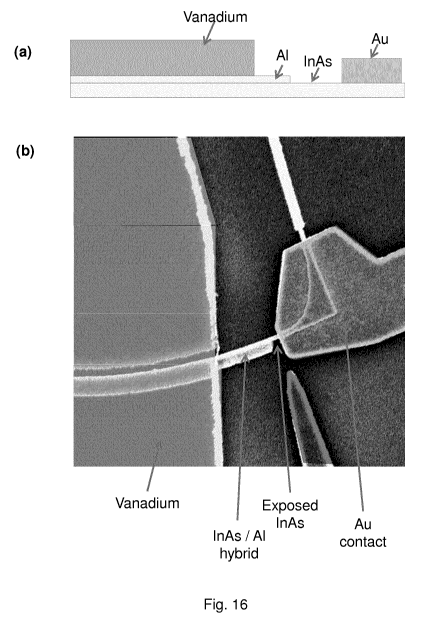
A double facet layer nanoscale device has been realized and characterized.
Fig. 16a
illustrates the schematic principle of an actual device with two facet layers
(aluminium
and vanadium) and a gold contact. Fig. 16b shows a picture of the actual
device. The
gap properties of the device in fig. 16b has been measured and are illustrated
in fig.
17a-c. The gap is appearing above 4 Kelvin. At low temperatures the gap is a
hard gap
(factor -100) with a gap magnitude of A* = 700 meV which is almost four times
larger
than that of aluminum in the case of a single facet layer device.
For some compounds making a good contact between the first and second facet
layers
may be a problem. For example the ceramic high-Tc superconductors need oxygen
when deposited as the second facet layer, which will inevitably oxidize the
first facet
layer in the case of e.g. aluminum. In such cases, adding a thin (approx. 0.3-
10
nanometers) layer of an inert materiel, such as gold or another inert metal,
such as
Platinum, Iridium, Palladium, Osmium, Silver, Rothenium or Rhodium, in order
to form
a spacer between the first and second facet layers, is desirable in order to
protect the
surface of the first facet layer. A further embodiment of the presently
disclosed
nanoscale device therefore comprises a third facet layer (or intermediate
layer or
interface layer) located between the first facet layer and the second facet
layer. The
third facet layer is preferably an inert material, such as a Noble metal, such
as Gold or
Platinum or Iridium or Palladium or Osmium or Silver or Rothenium or Rhodium.
Further, the thickness of the third facet layer is less than 10 nm, or less
than 5 nm, or
less than 4 nm, or less than 3 nm, or less than 2 nm, or less than 1 nm, or
less than 0.5
nm. In case of e.g. Gold it can be added directly in the MBE or subsequently
by
evaporation. If the thickness of the third facet layer is thin enough the
properties of the
CA 02953264 2016-12-21
WO 2016/001365 PCT/EP2015/065110
28
triple layers (first, third and second facet layers) will remain dominated by
the thicker
second facet layer.
Example 1 ¨ Semiconductor-metal epitaxy
The InAs nanowires are grown in two different axial crystal directions: the
'conventional' [0001]13, having six {1-100} sidefacets, and one of the six
equivalent <1-
100>wz (or <11-2>zs) directions having a rectangular cross section with two
(0001)6/(0001)A sidefacets and two {11-20} sidefacets. The Al phase is grown
at a
substrate temperature of -30 C which is the lowest achievable in the MBE
system
used, i.e. without the use of a dedicated cooling source. For growth on the
facets of the
conventional nanowires we report on three different types of metal growths:
one where
the substrate was rotated, resulting in growth on all six sidefacets, and two
types of
growths with no substrate rotation, oriented for growth on either two or three
facets.
Fig. 2 a, d and f show high-resolution TEM images of the most characteristic
epitaxial
match corresponding to three different types of the InAs/AI nanowires: the
<0001> InAs
nanowires with hsu 10 nm Al (Fig. 2a), <0001> nanowires with hsu 30 nm Al
shells
(Fig. 2d), and <01-10> nanowires with Al on the (111)B facet (Fig. 2f),
respectively.
Critical parameters linked to especially the low temperature electrical
properties,
depends on the thickness of the crystal phases and therefore on the overall
morphologies of the Al shells. Examples are shown in the TEM images of Fig. 3
for
three (two) different growths on <0001> (<01-10>) InAs nanowires with varying
thickness of the Al. For thin half shell of Al (hsu < 10 nm ) on the <0001>
nanowires
and on the <01-10> nanowires in general, the surface of the Al is smooth.
For a thick Al shell (hsu > 15nm ) on the facets on the <0001> nanowires, the
surface
of the Al becomes faceted (Fig. 3b and c). In the half-shell geometry, the Al
usually
causes the hybrids to bend either towards or away from the Al-covered side
providing
indirect information about the interface mismatch. As an example, Fig. 3f
shows an
SEM image for the case of a nanowire with 10 nm Al grown on two facets. The
nanowire bends towards the Al and thus suggests an interface with compressive
(tensile) strain in the InAs (Al). To explain the strain induced in the
crystals, we need to
discuss the epitaxial relation and ordering of the SE/M interfaces in terms of
domain
matching. That is, when a lattice mismatch of a given SE/M material
combination is
large, interfacial domains - consisting of nm and nsE interfacial units of M
and SE - form,
CA 02953264 2016-12-21
WO 2016/001365 PCT/EP2015/065110
29
in order to reduce the stress associated with the mismatch2. We describe a
given SE/M
( n (
interface with the interfacial domain notation: 114, __ x n'14 -L ,
where
n
\,nSE, y \,nSE,1 y SE
denotes the ratio of units in two orthogonal directions in the interfacial
plane parallel
and transverse 1 to the nanowire axis. e, is the corresponding residual
mismatch in
the respective directions as expected from relaxed structures at room
temperature. In
Fig.2 (b, c, e, g) is show simulations of three different types of interfaces
with relaxed
structures meeting in the interfacial plane, corresponding to the preferential
bicrystal
orientations that has observed in three different types of nanowires.
Considering the
epitaxial match at the InAs/AI interface for the thin Al shell on two facets
(Fig. 2a), there
are two obvious candidates in this orientation: either a small domain
(3 (3
[11-2] 6.5% x 3[1-10] ,0.3% that gives a large mismatch along the nanowire
axis,
\,2[11-20]
(7 (3
or a larger domain [h12]_0.5% x ____ ,0.3% with a smaller mismatch. The
two
cases are simulated in Fig. 2b and c, respectively. However, as shown in Fig.
3f, the
hybrid structure bends towards the Al, suggesting that the negative and much
smaller
mismatch of the 7/5 interfacial domain along the nanowire length is formed.
Surprisingly it was found that for the thick shell hybrids (Fig. 2d and Fig.
3c) the
preferential crystal structure is different with an out of interfacial plane
orientation of
(11-2). This gives a small and remarkably well matched
( 1 (3
"11] _________ ,0.3% x ,0.3% domain, as simulated in Fig. 2e.
\,1[0001] \] 2[11-20]
Fig. 2f shows the (111)zB//(111) interface formed on the topfacet of the <11-
2> InAs
wires. Again, the Al forms with the (111) out-of-plane orientation and keeps
this
orientation also for thicker Al shells (Fig. 2d, e). This match provides not
only a planar
and uniform film due to a (111) out of plane orientation, but also a highly
ordered
3 3
epitaxial domain match, [11-2] 0.3% x [1-10] 0.3% , with only a
slightly positive
[11-2]õ 2[1-10]zB
CA 02953264 2016-12-21
WO 2016/001365 PCT/EP2015/065110
strain along the nanowire length, consistent with an observed bending away
from the
Al.
For a given out of plane orientation there exist a number of distinguishable
grains with
5 indistinguishable interfacial domains. This is a consequence of the order
of the plane
PRSrotational symmetries (PRS) of SE and M, CiPsi6E'l and C which are not
necessarily the same as the order of the corresponding bulk rotational
symmetries,
ClIsE and C11,1,4 . In general, for a given type of SE M interface i, the
number of
distinguishable degenerate crystal orientations (variants) in M, is given as
sREs ip,mRs
10 m = __________________________________________ (2)
where (CiT,Ct'sRus ) is the least common multiple of CIP,sR5E and CIP,sR5u.
All three types of interfaces in Fig. 2 have a two-fold degeneracy, meaning
that two in-
plane orientations will nucleate with equal probability. These two variants
have been
15 seen for the (1-100)//(111) match in nanowires with a thin shell of Al
on two facets, and
in Fig. 4a, the two orientations are seen for (1-100)//(11-2) orientation with
a thick full
shell, consistent with equation (2). However, in the thick full shell devices
only rarely
are grain boundaries seen in the crystal structure around the nanowires.
20 To explain the formation of the different crystal structure orientations
as function of
phase thickness and type of device (full shell, half shell, etc.), the
essential
mechanisms can be understood using two independent parameters:{X}E thm,,Rm,I,
where hm, is the average grain thickness and Rm, is the average in-plane
radius of
curvature. While hm, plays an important role in the formation of the overall
morphology,
25 we are here interested in the mechanisms leading to grain growth, which
are driven
mainly by RM. It is convenient to separate the excess free energy into two
contributions: the excess free energy which arises from the bonding at the
interfaces,
and what arise from coherent strain or misfit dislocations due to lattice or
domain
mismatch. The corresponding driving force for the grain growth in the thin
film regime
30 relative to an average grain of the metal phase, M, is given by
CA 02953264 2016-12-21
WO 2016/001365 PCT/EP2015/065110
31
2frvinv K2 Se 2 R -
8 duitiRm, = i=-=2, srsurface,M' + 7SEI1M '
hm, s Rm, (1¨v)
where Q., is the atomic volume, Y
, suiface,M ' , 7SE1114 ' and 2111m. are the free energy
densities of the surface (per nanowire length), the SEIM' interface, and the
grain
boundaries, respectively. S is the shear modulus, v is Poisson's ratio and
strain
parameter defined as, e2 E C2 + C 2 + 2ve el. When 4um, = 0, the grain size of
M'
stays constant on average, while 4um, > 0 and gdum, <0 imply an average
driving force
for elimination and expansion, respectively. For the epitaxial growth of
planar
bicrystals, the host crystal is presumed to be a fixed inflexible reference
crystal for
which the growing crystal has to adapt to.
If the host crystal is a nanowire, it can also be considered as a fixed
reference in terms
of crystal structure, orientations, and overall faceting, however, unlike the
case of two-
dimensional planar growth, its finite size allows compression, stretching or
bending,
which play an important role in the strain relaxation of the whole complex,
and
therefore on thee parameter. SE M interfaces with a high interfacial order
(small
domains with small residual mismatch) are generally also interfaces with a
relative low
interfacial free energy, not only because of the contributions from coherency
strain
and/or misfit dislocations, but also because it is easier to form an
electronic match with
a low chemical energy. However, it is not necessarily also the corresponding
grain
orientations with the highest probability of formation, since, according to
equation (1),
many factors play a role during growth.
In the initial stage of the metal growth, islands forms at the semiconductor
surface,
where the substrate temperature plays an important role on the spacing between
the
islands. If the temperature is low enough, the spacing is so small that the
islands will
merge at very thin film thicknesses, which according to equation (1) will lead
to surface
driven grain growth.
As the metallic phase grows thicker, the surface-to-volume ratio decreases,
and the
last two terms of equation (1) become increasingly important. The stress
induced from
the InAs/A1 interface and from incoherent grain boundaries meeting on a
sidefacet or
across adjacent sidefacets provide a driving force for reconstruction into a
less strained
and lower total energy configuration. In Fig. 3a, b and c, a transition is
observed for half
CA 02953264 2016-12-21
WO 2016/001365 PCT/EP2015/065110
32
shell devices around hsu 20 nm to a more faceted Al surface having primarily
(112)
out of plane orientations at the interface (Fig. 3d).
For thick full shell devices (Fig. 4), the out-of-plane orientation is (11-2)
as in the case
shown in Fig. 2d, which gives two variants according to Eq. (1). In the
following the two
variants are labelled a and p. Along the nanowire axis, the InAs and Al have a
six-fold
and three-fold rotational symmetry, respectively. Thus, two Al grains put
together by a
six-fold rotation lead to incoherency. However, if the variants alternate
around the
nanowire, it will form a single crystal with <1-100>11<11-2> type domains on
all six
sidefacets (Fig. 4d). Only because the 6-fold rotational symmetry of WZ
nanowire axis
is really a screw axis the perfect bicrystal symmetry is broken (Fig. 4f),
which may
induce a small additional strain field around the edge where the sidefacets
meets.
Since, the Al growth preferentially start forming (111) out of plane
orientated grains,
which eventually reconstructs into other orientations, and eventually into (1-
100)11(112)
a and p variants, it is striking that single crystals can be observed all
along the hybrids,
as shown in Fig. 4a for the thick full shell nanowire. This can be understood
from
equation (2), since incoherent grain boundaries within the Al induce high
interfacial
energies (large yivillivi,) as compared to coherent boundaries, which gives a
strong
driving force for grain reconstruction to eliminate incoherencies. Thus if
grains of the
same variant nucleate on adjacent facets, the resulting incoherent interface
may drive
an elimination/reconstruction of the smaller on expense of the larger.
However,
kinetically locked incoherent interfaces are possible as shown in Fig. 4e, and
are
appearing frequently. For the grain boundaries meeting along the direction of
the
nanowire, a and p variants form low energy coherent twin boundaries, which do
not
lead to a driving force which is strong enough to eliminate the grain
boundaries.
Having established the feasibility of MBE to grow high quality InAs/A1
interfaces, it
opens for the possibility of controlled formation of contact barriers. This
can be
important for many types of possible applications, as barriers of high band-
gap
materials are routinely inserted into heterostructures in semiconductor
technology. An
important example can be in the formation of semiconductor-superconductor
hybrid
devices, where it has been predicted to enhance the magnitude of the induced
proximity gap, and also to minimize the amount of quasi-particle poisoning. We
demonstrate this method for the InAs/A1 hybrids by intentionally growing a 3
nm
segment of high band-gap AlAs (band gap of 2.12eV) at the interface, using
what we
CA 02953264 2016-12-21
WO 2016/001365 PCT/EP2015/065110
33
interpret as a backward growth mode. In Fig. 4g, the AlAs is clearly seen as a
change
in contrast in the TEM image and are verified by Electron Dispersive X-ray
analysis and
analysis of lattice spacings.
To study the electrical coupling between the shell and the InAs, devices were
fabricated where the core was exposed by selectively etching a segment of the
Al
between the contacts. The nanoscale device is illustrated in the insets to
Fig. 5d. The
exposed semiconductor becomes susceptible to electrostatic gating, and the
device
appears as a nanowire field effect transistor with the Al shell acting
contacts. Figure 5d
shows measured conductance as a function of the voltage Vg applied to the
conducting
back plane for various temperatures above T. As is generally observed, the
undoped
InAs nanowire acts as an n-type semiconductor and is depleted at Vg = -10V and
the
conductance increases with Vg to 2.8 e2/h at Vg = 10V. Other devices with
shorter
exposed InAs segments had conductivities up to 6 e2/h at Vg = 10V. These
values are
comparable to the best results we have achieved for devices of comparable
lengths
and diameters using conventional contacting schemes with either HF etching,
(NH4)2Sx
passivation, or argon milling for removing the native InAs oxide prior to
metal
evaporation. This indicates that the epitaxial shell forms a barrier-free
metal/semiconductor contact as is further supported by the temperature
dependence of
the transfer curves: For Vg > 2V the conductance increases upon cooling due to
the
reduction of phonon scattering rather, than decreases as is most often
observed for
imperfect contacts due to the reduction of thermally excited transport over
contact
barriers.
Example 2 - Superconducting properties
As seen in example 1 InAs and Al can form a highly ordered epitaxial domain
match.
In continuation hereof InAs/A1 is an interesting material system for
topological SE/SU
quantum devices because of the large spin orbit coupling in InAs and large
superconducting coherence length in Al.
Four-terminal devices were therefore fabricated on an InAs nanowire with a
13nm Al
full shell. Figs. 5a and b show the device schematic and SEM micrograph of the
device,
respectively. The inset in Fig. Sc shows the temperature dependence of the
four-
terminal resistance. The Al shell remains intact along the wire and the
resistance is
505/ for temperatures above -1.6K below which there is gradual transition to a
052.
superconducting state which is fully developed at -1.3K. The main panel of
fig. Sc
CA 02953264 2016-12-21
WO 2016/001365 PCT/EP2015/065110
34
shows the resistance of the Al shell as a function of a magnetic field applied
parallel to
the nanowire. For low fields, the resistance vanishes as expected for a
superconductor,
and the zero-resistance state persists up to 1.3 Tesla, only interrupted by
finite
resistance peaks at half-multiples of flux-quanta threading the wire. The
latter
phenomenon is related to the full-shell topology and is the well-known Little-
Parks
effect of superconductors in a double connected geometry. The oscillations
only occur
as long as the shell is in the superconducting state, and thus the shell has a
critical
magnetic field Bc -1.9T consistent with the results for a 13 nm thick planar
Al film.
However, the technique developed above for InAs/AI hybrids is not restricted
to this
particular choice of materials and the theoretical formalism is generally
applicable. As a
first approximation combinations where metal grains with <112> out of plane
orientations match InAs, and InSb semiconductor nanowires grown in the
conventional
<0001>wz or <111 >zg directions can be suggested. As described above, the
symmetries of this orientation are particularly appealing and allow single
coherent
grains to match the semiconductor across multiple facets. It can therefore be
expected
that these orientations to be likely to occur in the thick film limit if they
are matched in a
given SE/M system. In addition to the InAs/AI system (2/3 domain ratio, 0.3%
strain),
other noteworthy well-matched combinations include InAs/Au (2/3 domain ratio,
1.0%
strain) which may serve as model contact materials for non-superconductive
applications, and InAs/V (1/2 domain ratio, 0.3% strain) and InSb/Nb (1/2
domain ratio
1.8% strain) which are important combinations for high-critical temperature
and
magnetic field superconducting contacts to strong spin-orbit semiconductors.
For temperatures below the superconducting transition temperature the Al
shells
induces a superconducting gap into the InAs by virtue of the proximity effect.
In
contrast to all previous studies, however, the induced gap remains hard i.e.,
free of
sub-gap states, likely due to the perfectly uniform InAs//A1 interface. The
presently
disclosed nanoscale devices thereby remove a main obstacle for using
semiconductor
nanowires as the backbone in future schemes of topological quantum information
based on Majorana Fermions. In this context it is noted that the
InAs//Alepitaxial
hybrids fulfill all basic requirement remaining for use in Majorana devices:
strong spin-
orbit coupling, large critical parallel magnetic field, and gate-tunability.
CA 02953264 2016-12-21
WO 2016/001365 PCT/EP2015/065110
Example 3¨ Hard gap in epitaxial superconductor-semiconductor nanowires
Key signatures of topological superconductivity and associated Majorana end
states,
including a characteristic zero-bias tunneling peak appearing at finite
magnetic field,
have been reported in the prior art over the past few years. In all cases, a
soft gap is
5 also seen, indicated by sizable subgap conductance. The origin of the
soft gap is not
fully understood, with recent theory attributing it to disorder at the
semiconductor/superconductor interface, combined with inverse proximity effect
at the
normal-metal tunnel barrier. Besides complicating an already complex
mesoscopic
system by allowing alternative (Kondo) processes that can themselves give rise
to
10 zero-bias tunneling peaks, subgap states are fatal to topological
protection. This is
because quasiparticles occupying subgap states will inadvertently participate
in
braiding, thus influencing resulting quantum states in an unpredictable and
possibly
time-dependent way.
15 InAs nanowires were grown in the wurzite [0001] direction by molecular
beam epitaxy
(MBE) as also described above. After the nanowires reached a length of 5-10
pm, Al
was grown at low temperature by angled deposition within the MBE chamber. The
resulting semiconductor-superconductor interface, shown in Fig. 6c, appears
coherent,
domain matched, and impurity free. Rotating the substrate during Al growth
results in
20 full-shell nanowires (Fig. 6a); directional growth without rotating
yields half shell
nanowires, with Al on two or three facets of the hexagonal InAs core. The
nanowires
were then dispersed onto a doped Si substrate with a 100 nm oxide. The Al
shell was
contacted by superconducting Ti/AI (5/130 nm) and the InAs core (exposed with
a
selective Al etch) with normal Ti/Au (5/80 nm). Modest in situ ion milling was
used to
25 improve contact between both the core and shell to leads. A device
similar to the one
measured is shown in Fig. 6d. Control devices were fabricated by etching away
the Al
shell and evaporating Ti/AI in select areas (Figs. 6b and 6d). The 5 nm Ti
sticking layer
seemed to improve gap hardness in all control devices. A number of epitaxial
devices
and control devices were measured and showed similar behavior.
The carrier density in the exposed InAs was tuned via the backgate voltage,
VBG. The
additional side gate was not used (see Fig. 6b) in these measurements.
External
magnetic field, B, was applied along the nanowire, unless stated otherwise.
All
measurements were performed in a dilution refrigerator with a base temperature
of 20
mK. Devices into a tunneling regime (G << Go = 2e2/h) by reducing VBG. The
tunneling
spectra of a full-shell epitaxial device (blue) and an evaporated control
device (red) in
CA 02953264 2016-12-21
WO 2016/001365 PCT/EP2015/065110
36
the weak tunneling regime, with conductance of the exposed core tuned to G
<<G0 =
2e2/h are shown in Fig. 6e. In the superconducting state (B = 0), differential
conductance GS as a function of source-drain voltage, VSD, shows symmetric
peaks
with suppressed conductance between. Above a critical value of field, 13, (-75
mT for
epitaxial, ¨250 mT for control), both devices show a featureless normal-state
tunneling
conductances, GN, of approx. 0.01 e2/h. The ratio Gs/GN for both the epitaxial
and
control devices is shown in Fig. 6f. The positions of the peaks in GS indicate
a gap of
L.* = 190 peV, similar to the gap of bulk Al, and suppression by a factor of
approx. 100
of subgap conductance. The evaporated control device shows a slightly smaller
induced gap of 140 peV, and a suppression of subgap conduction by a factor of
approx. 5, comparable to previous measurements in InAs and InSb nanowires [10-
15].
Increasing VBG increases both subgap and above-gap conductances of the
epitaxial
full-shell device. A pair of subgap resonances (SGR) appears close to the gap
edge in
the range -11 V < VBG < -8 V (Fig. 7a). The appearance of this SGR coincides
with a
sharp increase in the above-gap conductance. The rest of the tunneling
spectrum is
devoid of other SGRs. In this device, no evidence of dot-like charging physics
was
observed (Fig. 7b). Conductance peaks independent of VBG occur at VSD = 190
pV, and
in some areas the subgap conductance exceeds the normal state conductance.
This
subgap conductance enhancement is illustrated in Fig. 7c, which shows two
vertical
cuts taken at low and high backgate voltages (indicated by orange and green
lines in
Figs. 7a and 7b). In Fig. 7d we plot the superconducting zero-bias conductance
as a
function of conductance at VSD = 0.4 mV. On the same graph is shown, with no
free
parameter, the theoretical dependence between Gs(Vsp = 0) and GN(Vsp = 0),
given by
the following expression in Blonder-Tinkham-Klapwijk-Beenakker (BTKB) theory:
N2
G = 2G0 G (1)
S võ,o
(2G0 ¨GN)2
The nanoscale device also exhibits conductance steps as a function of VBG
(Fig. 7e), a
typical signature of quantum point contacts (QPC). Zero-bias conductance in
the
normal state (black line) shows plateaus at values close to 1, 3, 6, and 10
e2/h. In the
superconducting state and at source-drain bias above ,8,*/e (red line), the
device
conductance shows a similar behavior, but begins to deviate above 6 e2/h.
Plateaus
are less defined at zero-bias in the superconducting state (green line).
Instead,
conductance oscillates around the normal state values and peaks on the lower
VBG
edge of the normal state plateaus. Not all of the measured devices, epitaxial
or
evaporated, form QPCs. Instead, a quantum dot (QD) can form in the exposed
InAs
CA 02953264 2016-12-21
WO 2016/001365 PCT/EP2015/065110
37
core (Fig. 8a). In the normal state of an epitaxial full-shell QD device,
Coulomb
diamond resonances and well defined even-odd structures can be identified (see
supplementary information). In the superconducting state, symmetric SGRs in
the
shape of inverted bells occupy the odd diamond valleys (Fig. 8b). These SGRs,
arising
from Andreev bound states (ABS) or Yu-Shiba-Rusinov states, have been
extensively
investigated in the prior art.
Similar QD structure and their associated SGRs in the superconducting state
are also
observed in the control devices. Vertical cuts at the particle-hole symmetry
point of an
odd (orange) and even (green) Coulomb valley are shown in Fig. 8c. Away from
the
SGRs, both even and odd Coulomb valley traces show highly suppressed subgap
conductances. We compare the normalized conductance of an epitaxial full-shell
QPC
device against an epitaxial full-shell QD device tuned to the middle of an
even Coulomb
valley (Fig. 8d). The two measurements are almost indistinguishable, and this
experimental observation allows us to compare induced gap measurements between
various devices, regardless of their QPC or QD nature. Since fabricated QPC
devices
are of a rarer variety than QD devices in nanowire systems, all comparisons
between
epitaxial and evaporated devices are between the epitaxial full-shell QPC
device and
an evaporated QD device.
In Figs. 9a and 9b we study the evolution of the induced gap as a function of
magnetic
field and temperature. We then compare the normalized zero-bias conductance of
an
epitaxial full-shell device against an evaporated control device in Figs. 9c
and 9d. Since
the subgap conductance in epitaxial devices is close to our experimental noise-
floor,
we average over a 40 pV window centered about zero-bias and define this value
as
G ) I G,';). Experimental error bars smaller than the marker size in Figs. 9c
and 9d are
not shown. For better comparison the applied magnetic field is normalized by
the
critical fields of each device in Fig. 9c. Fig. 9d shows the normalized zero-
bias
conductance as a function of temperature. We fit the temperature dependent
tunneling
conductance of a N-S junction in BCS theory to data from the epitaxial full-
shell device.
The theoretical dependence is given by the expression:
G 27rA* -A* IkBT
S
= \41- e (2)
GN vs = kBT
where kB is the Boltzmann constant and T is the temperature. From the
theoretical fit
(blue line), we extract an induced gap of 160 peV.
CA 02953264 2016-12-21
WO 2016/001365 PCT/EP2015/065110
38
Similar devices were fabricated on epitaxial half-shell nanowires (Fig. 10a,
10b, and
10d), with the exception that an additional Al lead is added to the device,
and these
leads now contact both the shell and the core. Identical tunneling
spectroscopy is
performed on these devices, and we compare the induced gap quality of the full-
shell
QPC device to a half-shell QD device in Fig. 10c. The induced gap size of an
epitaxial
half-shell device (180 peV) is similar to the induced gap size in epitaxial
full-shell
devices. The normalized subgap conductance is a factor of 50 lower than the
normal
state conductance, substantially better than the induced gap in evaporated
control
devices.
The additional Al lead to the shell allows us to explore the gate-tunability
of the half-
exposed InAs core. As illustrated in Fig. 10b a current bias is applied
between the two
Al leads and the voltage drop is measured when the device is in the normal
state (B1=
100mT > Be). Conductance through the normal state Al shell and the
semiconducting
InAs core is shown in Fig. 10e. It remains roughly constant at 10 e2/h below
VBG = 3 V,
then rises to approximately 45 e2/h at much higher VBG. Normalized subgap
conductance suppression of up to two orders of magnitude represents a
significant
improvement in the hardness of induced gaps in InAs nanowires. This number
should
be regarded as a lower bound limited by the experimental noise floor of
measurement
set-up used (Fig. 6f). While the effects of a Ti sticking layer on the
hardness of the
proximitized gap cannot be isolated, it is noted that the control devices
fabricated
without the sticking layer have produced far inferior induced gaps. The
collective
measurements across multiple devices, epitaxial and evaporated, suggest that
the soft
gap is a result of semiconductor-superconductor interface roughness.
Commonly practiced methods of proximitizing these nanowires require the
removal of
native oxides either via chemical etching or physical ion-milling before the
deposition of
a superconducting metal. These fabrication steps can potentially damage the
crystalline semiconductor surface. Interface quality aside, the QPC nature of
the
presently disclosed epitaxial full-shell device demonstrates ballistic
transport in the
semiconducting core. The only SGR present in the QPC device (Fig. 2a)
coincides in
VBG with the first conductance plateau in the normal state. We interpret this
resonance
as an ABS formed from the first sub-band of a one-dimensional channel [36].
CA 02953264 2016-12-21
WO 2016/001365 PCT/EP2015/065110
39
In the tunneling limit the normal state conductance is approximated by the
quasiparticle
transport conductance measured at sufficiently high source-drain bias
(Vsp = 0.4 mV > .8:/e). Comparing this value against the zero-bias
superconducting
state conductance excellent agreement is found between experiment and BTKB
theory
(Fig. 7d). What is remarkable is that the comparison between experiment and
theory
has no free parameter. The zero-bias superconducting state conductance of a
single
channel N-S junction depends solely on the transmission coefficient, r, which,
in
Landauer formalism, is directly proportional to the normal state conductance.
Measurement noise notwithstanding, the striking similarity between experiment
and
theory tells us that the hardness of the induced gap is close to its
theoretical limit.
Further agreement with BTKB theory can be found by comparing subgap
conductances
between the tunneling regime and the open transport regime (Fig. 7c). At low
backgate voltages, the probability of Andreev reflection is low because of a
high tunnel
barrier (Fig. 8a, upper panel) between the normal lead and the proximitized
InAs core.
At high backgate voltages, the barrier is lowered and the subgap conductance
is
enhanced above its normal state value. However, it is noted that there remains
a finite
probability for an electron to specular reflect against the proximitized core.
This is
evident from the fact that the subgap conductance never reaches twice its
normal state
value.
Conductance steps as a function of backgate voltage are evident in Fig. 7e,
but the
steps do not occur at typical QPC values. The discrepancy could be attributed
to
imperfect transmission of one-dimensional conduction modes and additional
symmetries in the transverse confining potential of the nanowire. In addition,
while line
resistances have been subtracted from our measurement set-up, additional
contact
resistances within the device cannot be accounted for.
While QPCs and QDs represent vastly different transport regimes in a nanowire,
both
types of devices allow tunneling spectroscopy to be performed on the
proximitized
core. As illustrated in Fig. 8a, a QPC near pinch-off forms a single tunnel
barrier
between the normal electrode and the InAs core. On the other hand, a single QD
can
be envisioned as two tunnel barriers with discrete states in between. Since
the
charging energy of the reported QD device is larger than the induced gap .8:,
when
VBG is tuned to the particle-hole symmetry point of an even Coulomb diamond,
the
discrete QD states are far from the edge of the induced gap. The QD thus acts
as a
CA 02953264 2016-12-21
WO 2016/001365 PCT/EP2015/065110
single tunnel barrier between the normal lead and the proximitized InAs core.
The
agreement of tunneling spectroscopy measurements between the QPC and the QD
device (Fig. 8c) serves as an experimental validation of this interpretation.
In Fig. 9a
and 9c, it is noted that the floor of the induced gap remains close to zero,
rising sharply
5 only when B approaches B. Retaining a hard gap at finite magnetic fields
is an
important trait for Majorana bound state experiments since theoretical
framework
requires that the Zeeman energy in the semiconductor be larger than the
induced s-
wave pairing gap. While the temperature dependent tunneling conductance from
BCS
theory qualitatively fits the experimental observation (Fig. 10d), the
extracted induced
10 gap of 160 peV does not coincide with the tunneling spectroscopy
measurement of .8:=
190 peV. Alternatively, one can interpret this discrepancy as an effective
device
temperature that is roughly a factor of 1.2 larger than the measured
temperature of the
dilution refrigerator. Although the actual electron temperature can be higher
than the
cryostat temperature, the two values are expected to agree fairly well at
elevated
15 temperatures above 100 mK.
Turning the attention to the epitaxial half-shell variety of nanowires, it is
found that the
induced gap has similar hardness to their full-shell cousins (Fig. 10c). More
interestingly, in the normal state of the Al shell, the conductance between
the two Al
20 leads is gate-dependent. The resistance saturates at about 2.5 k52,
below VBG = 3 V,
and lowers to about 600 5/ at higher backgate voltages (Fig. 10e). The
saturated
resistance is interpreted to be the resistance of the Al shell, and the
subsequent
reduction of resistance to come from the opening of a parallel conduction
channel
through the InAs core. The following transport parameters are estimated for
the InAs
25 core: (i) carrier density (at high VBG), n = 5 x 1018cm-3 (ii) mobility,
p = 3300 cm2/Vs (iii)
elastic scattering length, le = 100 nm. These are typical values for InAs
nanowires.
However, the expected resistance for the present Al shell should be on the
order of 10
a The higher measured resistance could be attributed to additional contact
resistance
between the Al leads and the Al shell.
While epitaxial full-shell nanowires provide interesting geometries
(cylindrical
superconducting shell) for future experiments, it is probably the epitaxial
half-shell
variety that strongly interests the Majorana community. The possibility of
controlling the
sub-band occupation in a large spin-orbit, large g-factor quasi-one-
dimensional
semiconductor while maintaining a hard induced superconducting gap makes the
epitaxial half-shell nanowire an ideal platform for nanowire-based Majorana
qubits.
CA 02953264 2016-12-21
WO 2016/001365 PCT/EP2015/065110
41
Further details
1. A nanoscale device comprising an elongated crystalline nanostructure, such
as
a nanowire (crystal) or nanowhisker (crystal) or nanorod (crystal), having a
plurality of substantially plane side facets and a first facet layer covering
at least
a part of one or more of said side facets.
2. The nanoscale device according to item 1, wherein the first facet layer is
crystalline.
3. The nanoscale device according to any of preceding items, wherein the two-
dimensional interface between a side facet of the crystalline nanostructure
and
the first facet layer is epitaxial.
4. A nanoscale device comprising an elongated crystalline semiconductor
nanostructure, such as a nanowire (crystal) or nanowhisker (crystal) or
nanorod
(crystal), having a plurality of substantially plane side facets and a
crystalline
structured first facet layer of a superconductor material covering at least a
part
of one or more of said side facets, and wherein the crystalline structure of
the
semiconductor nanostructure is epitaxially matched with the crystalline
structure
of the first facet layer on the interface between the two crystalline
structures.
5. The nanoscale device according to any of preceding items, wherein the two-
dimensional interfaces between each side facet of the crystalline
nanostructure
and the first facet layer are epitaxial, such as simultaneously epitaxially
matched.
6. The nanoscale device according to any of preceding items, wherein each two-
dimensional interface between a side facet of the crystalline nanostructure
and
the first facet layer are domain matched and/or lattice matched in at least
one
dimension.
7. The nanoscale device according to any of preceding items, wherein each two-
dimensional interface between a side facet of the crystalline nanostructure
and
the first facet layer are domain matched and/or lattice matched in both
dimensions.
CA 02953264 2016-12-21
WO 2016/001365 PCT/EP2015/065110
42
8. The nanoscale device according to any of preceding items, wherein the
crystalline structure of the nanostructure is epitaxially matched with the
crystalline structure of the first facet layer.
9. The nanoscale device according to any of preceding items, wherein the
nanostructure is an elongated hybrid nanostructure comprising a crystalline
semiconductor nanostructure and wherein the first facet layer is a crystalline
structured layer of a of superconductor material and wherein the crystalline
structure of the semiconductor nanostructure is epitaxially matched with the
crystalline structure of the first facet layer on the interface between the
two
crystalline structures.
10. The nanoscale device according to any of preceding items 9, wherein the
epitaxial match and the proximity between the crystalline structures of the
semiconductor nanostructure and the first facet layer is configured to induce
a
superconductor hard gap in the semiconductor nanostructure.
11. The nanoscale device according to any of preceding items 9-10, wherein the
epitaxial match between the crystalline structures of the semiconductor
nanostructure and the superconductor first facet layer and the proximity and
superconductor properties of the second facet layer are configured to induce a
superconductor hard gap in the semiconductor nanostructure
12. The nanoscale device according to any of preceding items, wherein each two-
dimensional interface between a plane surface of the nanostructure and the
first
facet layer is domain matched and/or lattice matched in at least one
dimension.
13. The nanoscale device according to any of preceding items, wherein the
crystal
structure of the elongated crystalline nanostructure and the crystal structure
of
the first facet layer belong to different lattice systems.
14. The nanoscale device according to any of preceding items, wherein the
Bravais
lattice of the elongated crystalline nanostructure is different from the
Bravais
lattice of the first facet layer.
CA 02953264 2016-12-21
WO 2016/001365 PCT/EP2015/065110
43
15. The nanoscale device according to any of preceding items, wherein the
crystal
structure of the elongated crystalline nanostructure is selected from the
group of
zincblende and wurtzite.
16. The nanoscale device according to any of preceding items, wherein the
crystal
structure of the first facet layer is selected from the cubic crystal system,
such
as primitive cubic, BCC or FCC, or orthorhombic, trigonal, tetragonal or
perovskite.
17. The nanoscale device according to any of preceding items, wherein the
first
facet layer comprises one or more large single crystal segments wherein the
interface between the elongated crystalline nanostructure and said single
crystal segment(s) is epitaxially matched, such as simultaneously epitaxially
matched on all side facets.
18. The nanoscale device according to any of preceding items, wherein the
elongated crystalline nanostructure is substantially one-dimensional.
19. The nanoscale device according to any of preceding items, wherein the
elongated crystalline nanostructure is formed from branched nanowhisker
crystals.
20. The nanoscale device according to any of preceding items, wherein the
elongated crystalline nanostructure comprises one or more kinks.
21. The nanoscale device according to any of preceding items, wherein the
crystalline nanostructure is a single crystal.
22. The nanoscale device according to any of preceding items, wherein the
crystalline nanostructure comprises one or more large single crystal segments.
23. The nanoscale device according to any of preceding items, wherein the
crystalline facet layer comprises one or more large single crystal segments,
such as single crystal segments having an extension of at least 20 nm, or
least
30 nm, or at least 40 nm, or at least 50 nm.
CA 02953264 2016-12-21
WO 2016/001365 PCT/EP2015/065110
44
24. The nanoscale device according to any of preceding items, wherein the
crystalline nanostructure is composed of one or more crystals.
25. The nanoscale device according to any of preceding items, wherein the
crystalline nanostructure is a heterostructured nanowire crystal.
26. The nanoscale device according to any of preceding items, wherein the
crystalline nanostructure is a heterostructured nanowire crystal composed of
varying compounds in the axial and/or radial direction.
27. The nanoscale device according to any of preceding items, wherein the
crystalline nanostructure is provided in a semiconducting material.
28. The nanoscale device according to any of preceding items, wherein the
crystalline nanostructure is provided in a semiconducting material selected
from
the collection of group 111-V combinations, such as InAs, InP, InSb, GaAs,
GaSb, AlSb and InGaAs, or group IV elements such as Si or Ge, or group IV
combinations such as SiGe, or group 11-V1 combinations such as ZnO, ZnSe
and CdSe, or group 1-VII combinations.
29. The nanoscale device according to any of preceding items, wherein the
first
facet layer is a metal.
30. The nanoscale device according to any of preceding items, wherein the
first
facet layer is provided in a material with superconducting properties below a
critical temperature T.
31. The nanoscale device according to any of preceding items, wherein the
first
facet layer is a metal selected from the group of Al, Ne, Ar, Ca, Ni, Cu, Kr,
Sr,
Rh, Pd, Ag, Xe, Ce, Yb, Ir, Pt, Au, Pb, Ac, Th, Li, Na, K, V, Cr, Fe, Rb, Nb,
Mo,
Cs, Ba, Eu, Ta and W.
32. The nanoscale device according to any of preceding items, wherein the
cross-
section of the crystalline nanostructure is square providing a total of four
side
facets.
CA 02953264 2016-12-21
WO 2016/001365 PCT/EP2015/065110
33. The nanoscale device according to any of preceding items, wherein the
cross-
section of the crystalline nanostructure is hexagonal providing a total of six
side
facets.
5 34. The nanoscale device according to any of preceding items, wherein the
first
facet layer is covering at least a part of 1, 2, 3, 4, 5, 6 or more of the
side facets.
35. The nanoscale device according to any of preceding items, wherein the
thickness of the first facet layer is less than 300 nm, or less than 250 nm,
or
10 less than 200 nm, or less than 150 nm, or less than 100 nm, or less
than 90 nm,
or less than 80 nm, or less than 70 nm, or less than 60 nm, or less than 50
nm,
or less than 45 nm, or less than 40 nm, or less than 35 nm, or less than 30
nm,
or less than 25 nm, or less than 20 nm, or less than 19 nm, or less than 18
nm,
or less than 17 nm, or less than 16 nm, or less than 15 nm, or less than 14
nm,
15 or less than 13 nm, or less than 12 nm, or less than 11 nm, or less
than 10 nm,
or less than 9 nm, or less than 8 nm, or less than 7 nm, or less than 6 nm, or
less than 5 nm.
36. The nanoscale device according to any of preceding items, wherein the
20 diameter of the crystalline nanostructure is between 10 and 200 nm,
such as
between 10 and 20 nm, or between 20 and 30 nm, or between 30 and 40 nm,
or between 40 and 50 nm, or between 50 and 60 nm, or between 60 and 70
nm, or between 70 and 80 nm, or between 80 and 90 nm, or between 90 and
100 nm, or between 100 and 110 nm, or between 110 and 120 nm, or between
25 120 and 140 nm, or between 140 and 160 nm, or between 160 and 180 nm,
or
between 180 and 200 nm.
37. The nanoscale device according to any of preceding items, wherein the
length
of the crystalline nanostructure is between 1 and 20 lim, or between 1 and 2
30 lim, or between 2 and 3 lim, or between 3 and 4 lim, or between 4 and
5 lim, or
between 5 and 6 lim, or between 6 and 7 lim, or between 7 and 8 Jim, or
between 8 and 9 Jim, or between 9 and 10 Jim, or between 10 and 12 um, or
between 12 and 14 Jim, or between 14 and 16 Jim, or between 16 and 18 Jim,
or between 18 and 20 um.
CA 02953264 2016-12-21
WO 2016/001365 PCT/EP2015/065110
46
38. The nanoscale device according to any of preceding items, further
comprising a
second facet layer covering at least a part of the first facet layer.
39. The nanoscale device according to any of preceding items 38, the first
facet
layer having a crystalline structure which is epitaxially matched with the
crystalline structure of the nanostructure.
40. The nanoscale device according to any of preceding items 39, the second
facet
layer having a crystalline structure which is not epitaxially matched with the
crystalline structure of the nanostructure.
41. The nanoscale device according to any of preceding items 38 to 40, wherein
the crystalline nanostructure is provided in semiconducting material, the
first
facet layer is provided in a first material with superconducting properties
below
a first critical temperature, and the second facet layer is provided in a
second
material with superconducting properties below a second critical temperature.
42. The nanoscale device according to any of preceding items 41, wherein the
first
critical temperature is lower than the second critical temperature.
43. The nanoscale device according to any of preceding items 38 to 42, wherein
the thickness of the first facet layer is less than 20 nm, or less than 10 nm,
more
preferred less than 8 nm, more preferred less than 6 nm, more preferred less
than 5 nm.
44. The nanoscale device according to any of preceding items 38 to 43, wherein
the thickness of the second facet layer is at least 50 nm, or greater than 100
nm, or greater than 150 nm, or greater than 200 nm, or greater than 300 nm.
45. The nanoscale device according to any of preceding items 38 to 43, wherein
the thickness of the second facet layer is at least two times the thickness of
the
first facet layer, or at least 3, 4, 5, 6, 7, 8, 9 or at least 10 times the
thickness of
the first facet layer.
46. The nanoscale device according to any of preceding items 38 to 44, further
comprising a third facet layer located between the first facet layer and the
CA 02953264 2016-12-21
WO 2016/001365 PCT/EP2015/065110
47
second facet layer.
47. The nanoscale device according to any of preceding items 46, wherein the
third
facet layer is an inert material, such as an inert metal, selected from the
group
of gold, platinum, iridium, palladium, osmium, silver, rothenium and rhodium.
48. The nanoscale device according to any of preceding items 46 to 47, wherein
the thickness of the third facet layer is between 3 and 10 nm, or less than 10
nm, or less than 5 nm, or less than 4 nm, or less than 3 nm, or less than 2
nm,
or less than 1 nm.
49. The nanoscale device according to any of preceding items 38 to 48, wherein
the first facet layer is a metal selected from the group of Al, Ca, Ni, Cu,
Kr, Sr,
Rh, Pd, Ag, Ce, Yb, Ir, Pt, Au, Pb, Ac, Th, Li, Na, K, V, Cr, Fe, Rb, Nb, Mo,
Cs,
Ba, Eu, Ta and W.
50. The nanoscale device according to any of preceding items 38 to 49, wherein
the first facet layer is Al.
51. The nanoscale device according to any of preceding items 38 to 50, wherein
the second facet layer is a metal selected from the group of Al, Ca, Ni, Cu,
Kr,
Sr, Rh, Pd, Ag, Ce, Yb, Ir, Pt, Au, Pb, Ac, Th, Li, Na, K, V, Cr, Fe, Rb, Nb,
Mo,
Cs, Ba, Eu, Ta and W.
52. The nanoscale device according to any of preceding items 38 to 51, wherein
the second facet layer is an alloy, such as an alloy selected from the group
of
MgB2, niobium alloys, such as NiTi, NbTiN with various fractions of Ti and N,
and Zr100_xMx where x is any number in the range of 0 to 100 and M is a metal
selected from the group of Fe, Co, Ni, Cu, Ru, Rh, Pd, Os, Ir, Pt and Au.
53. The nanoscale device according to any of preceding items 38 to 51, wherein
the second facet layer is a ceramic material, such as selected from the group
of
cuprates, such as YBCO (YBa2Cu307-).
54. The nanoscale device according to any of preceding items 38 to 53, wherein
the second facet layer is a material with superconducting properties below a
CA 02953264 2016-12-21
WO 2016/001365 PCT/EP2015/065110
48
critical temperature.
55. The nanoscale device according to any of preceding items 38 to 54, wherein
the crystalline nanostructure is provided in a semiconducting material.
56. The nanoscale device according to any of preceding items 38 to 55, wherein
the crystalline nanostructure is provided in a semiconducting material
selected
from the collection of group 111-V combinations, such as InAs, InP, InSb,
GaAs,
GaSb, AlSb and InGaAs, or group IV elements such as Si or Ge, or group IV
combinations such as SiGe, or group 11-V1 combinations such as ZnO, ZnSe
and CdSe, or group 1-VII combinations.
57. A quantum point contact comprising the nanoscale device according to any
of
preceding items having a semiconducting core and a superconducting facet
layer.
58. The quantum point contact according to item 57, comprising
- a first section where the semiconducting core has been exposed
and
brought in contact with a normal conductor, such as Au,
- a second section where the semiconducting core is exposed, and
- a third section wherein the superconducting surface of the
nanoscale device
is brought in contact with a superconductor.
59. A superconducting field effect transistor comprising one or more of the
nanoscale devices according to any of the preceding items.
60. A method for producing a nanoscale device comprising the steps of
a) growing, at an elevated temperature, one or more crystalline
nanostructures in the normal direction on a plane substrate,
b) lowering the temperature and optionally reducing the background
pressure,
c) further reducing the temperature thereby cooling the substrate with the
crystalline nanostructures to a temperature below 20 C, and
d) depositing, at said reduced temperature below -20 C, a first facet layer
directly on at least one side facet of the crystalline nanostructures.
CA 02953264 2016-12-21
WO 2016/001365 PCT/EP2015/065110
49
61. The method according to any of preceding method items, wherein the
crystalline nanostructure and the deposition of the first facet layer are
provided
by means of molecular beam epitaxy (MBE)
62. The method according to any of preceding method items, wherein the step of
growing crystalline nanostructure(s) is provided by means of the vapour liquid
solid (VLS) method.
63. A method for producing a nanoscale device in a vacuum chamber by means of
molecular beam epitaxy (MBE), the method comprising the steps of
a) growing, preferably by means of vapour liquid solid (VLS) growth, at an
elevated temperature of above 400 C, one or more elongated crystalline
nanostructures, such as nanowire (crystals), in the normal direction on a
plane substrate,
b) shutting off all sources of growth material and reducing the temperature
thereby cooling the substrate with the crystalline nanostructures to a
temperature below -30 C, and
c) depositing, at said reduced temperature below -30 C, a crystalline first
facet layer directly on at least one side facet of the crystalline
nanostructures by means of MBE.
64. The method according to any of preceding method items, wherein the plane
substrate is located in a vacuum chamber, e.g. MBE chamber, and prepared
with catalysing particles, such as Au particles.
65. The method according to any of preceding method items, wherein the
substrate
is rotated during deposition of the first facet layer to cover additional side
facets
of the crystalline nanostructures.
66. The method according to any of preceding method items, wherein the source
for the first facet layer is located at a finite angle to the normal direction
of the
substrate during deposition of said first facet layer.
67. The method according to any of preceding method items, wherein the
temperature of the substrate before and during deposition of the first facet
layer
is reduced to a temperature below 10 C, or below 0 C, or below -5 C, or below
CA 02953264 2016-12-21
WO 2016/001365 PCT/EP2015/065110
-10 C or below -15 C, more preferably below -20 C, yet more preferably below
-25 C, most preferably below -30 C.
68. The method according to any of preceding method items, wherein the
thickness
5 of the first facet layer is less than 50 nm, or less than 40 nm, or
less than 30
nm, more preferably less than 25 nm, even more preferably less than 20 nm,
and even more preferably less than 15 nm, yet more preferably less than 10
nm, most preferably less than 5 nm.
10 69. The method according to any of preceding method items, further
comprising the
step of kinking the growth direction of the crystalline nanostructure during
growing of said structure.
70. The method according to item 69, wherein the growth direction is kinked by
15 means of a short flush of Ga25 or by means of a short temperature drop
during
growing of the crystalline nanostructure.
71. The method according to any of preceding method items, wherein the step of
growing comprises growing the elongated crystalline nanostructure of the
20 nanoscale device according to any of preceding items 1-56.
72. The method according to any of preceding method items, wherein the step of
depositing comprising depositing the first facet layer of the nanoscale device
according to any of preceding items 1-56.
73. The method according to any of preceding method items, wherein the first
facet
layer is a metal selected from the group of Al, Ne, Ar, Ca, Ni, Cu, Kr, Sr,
Rh, Pd,
Ag, Xe, Ce, Yb, Ir, Pt, Au, Pb, Ac, Th, Li, Na, K, V, Cr, Fe, Rb, Nb, Mo, Cs,
Ba,
Eu, Ta and W.
74. The method according to any of preceding method items, further comprising
the
step of depositing a second facet layer covering at least a part of the first
facet
layer, the second facet layer being different from the first facet layer.
75. The method according to any of preceding method items 74, wherein the
material of the second facet layer is different from the material of the first
facet
CA 02953264 2016-12-21
WO 2016/001365 PCT/EP2015/065110
51
layer
76. The method according to any of preceding method items, wherein the first
facet
layer has a crystalline structure which is epitaxially matched with the
crystalline
structure of the nanostructure.
77. The method according to any of preceding method items 74-76, wherein the
second facet layer has a crystalline structure which is not epitaxially
matched
with the crystalline structure of the nanostructure.
78. The method according to any of preceding method items 74-77, wherein the
crystalline nanostructure is provided in semiconducting material, the first
facet
layer is provided in a first material with superconducting properties below a
first
critical temperature, and the second facet layer is provided in a second
material
with superconducting properties below a second critical temperature.
79. The method according to any of preceding method items 78, wherein the
first
critical temperature is lower than the second critical temperature.
80. The method according to any of preceding method items 74-79, further
comprising the step of depositing a third facet layer before depositing the
second facet layer, such that the third facet layer is located between the
first
facet layer and the second facet layer, the third facet layer being different
from
the first and second facet layers, preferably the material of the third facet
layer
is different from the materials of the first and second facet layers.
81. The method according to any of preceding method items 80, wherein the
third
facet layer is provided in an inert material, such as an inert metal, selected
from
the group of gold, platinum, iridium, palladium, osmium, silver, rothenium and
rhodium.
82. The method according to any of preceding method items 80 to 81, wherein
the
thickness of the third facet layer is between 3 and 10 nm, or less than 10 nm,
or
less than 5 nm, or less than 4 nm, or less than 3 nm, or less than 2 nm, or
less
than 1 nm.
CA 02953264 2016-12-21
WO 2016/001365 PCT/EP2015/065110
52
83. The method according to any of preceding method items 74-82, wherein the
second facet layer is a metal selected from the group of Al, Ca, Ni, Cu, Kr,
Sr,
Rh, Pd, Ag, Ce, Yb, Ir, Pt, Au, Pb, Ac, Th, Li, Na, K, V, Cr, Fe, Rb, Nb, Mo,
Cs,
Ba, Eu, Ta and W.
84. The method according to any of preceding method items 74-83, wherein the
second facet layer is an alloy, such as an alloy selected from the group of
MgB2, niobium alloys, such as NiTi, NbTiN with various fractions of Ti and N,
and Zr100_xMx where x is any number in the range of 0 to 100 and M is a metal
selected from the group of Fe, Co, Ni, Cu, Ru, Rh, Pd, Os, Ir, Pt and Au.
85. The method according to any of preceding method items 74-84, wherein the
second facet layer is a ceramic material, such as selected from the group of
cuprates, such as YBCO (YBa2Cu307-).
86. The method according to any of preceding method items 74-85, wherein the
second facet layer is a material with superconducting properties below a
critical
temperature.
87. The method according to any of preceding method items 74-83, wherein the
crystalline nanostructure is provided in a semiconducting material.
88. The method according to any of preceding method items, wherein the
crystalline nanostructure is provided in a semiconducting material selected
from
the collection of group 111-V combinations, such as InAs, InP, InSb, GaAs,
GaSb, AlSb and InGaAs, or group IV elements such as Si or Ge, or group IV
combinations such as SiGe, or group 11-V1 combinations such as ZnO, ZnSe
and CdSe, or group 1-VII combinations.
89. The method according to any of preceding method items, wherein the step of
depositing the second facet layer comprises depositing the second facet layer
of the nanoscale device according to any of preceding items 1-56.
90. The method according to any of preceding method items, wherein the step of
depositing the third facet layer comprises depositing the third facet layer of
the
CA 02953264 2016-12-21
WO 2016/001365
PCT/EP2015/065110
53
nanoscale device according to any of preceding items 1-56.
91. The method according to any of preceding method items, wherein the steps
of
growing and depositing of the first, second and/or third facet layer(s) are
provided by means of molecular beam epitaxy (MBE).
92. The method according to any of preceding method items, wherein the steps
of
growing and depositing of the first facet layers are provided by means of
molecular beam epitaxy (MBE), whereas the step of depositing the second
facet layer and/or the third facet layer is provided by means of a different
deposition process, such as evaporation, sputtering, pulsed laser deposition
or
chemical vapor deposition.
93. The method according to any of preceding method items, wherein at least
one
of said elongated crystalline nanostructures comprises at least one kink such
that said elongated crystalline nanostructures initially one section that is
normal
to the substrate and one section that is substantially parallel to the
substrate.
94. A nanoscale device obtained by the method according to any of preceding
method items.
95. A method for producing a metallic contact and/or interface to a
semiconductor
one-dimensional crystalline nanostructure (nanowire).
96. A nanoscale device obtained by the method according to any of preceding
items comprising one of said elongated crystalline nanostructures, such as a
nanowire (crystal) or nanowhisker (crystal) or nanorod (crystal), having a
plurality of substantially plane side facets and the crystalline facet layer
covering at least a part of one or more of said side facets.
97. The nanoscale device according to item 96, wherein each two-dimensional
interface between a side facet of the crystalline nanostructure and the first
facet
layer are epitaxially matched, domain matched and/or lattice matched in both
dimensions.
CA 02953264 2016-12-21
WO 2016/001365 PCT/EP2015/065110
54
98. The nanoscale device according to any of preceding items, wherein the
crystal
structure of the elongated crystalline nanostructure is selected from the
group of
zincblende and wurtzite.
99. The nanoscale device according to any of preceding items, wherein the
crystalline nanostructure is provided in a semiconducting material selected
from
the collection of group 111-V combinations, such as InAs, InP, InSb, GaAs,
GaSb, AlSb and InGaAs, or group IV elements such as Si or Ge, or group IV
combinations such as SiGe, or group 11-V1 combinations such as ZnO, ZnSe
and CdSe, or group 1-VII combinations.
100. The nanoscale device according to any of preceding items, wherein the
crystal structure of the first facet layer is selected from the cubic crystal
system,
such as primitive cubic, BCC or FCC, or orthorhombic, trigonal, tetragonal or
perovskite.
101. The nanoscale device according to any of preceding items, wherein the
first facet layer is provided in a material with superconducting properties
below
a critical temperature T.
102. The nanoscale device according to any of preceding items, wherein the
thickness of the first facet layer is less than 10 nm.
103. The nanoscale device according to any of preceding items, wherein the
first facet layer comprises one or more large single crystal segments wherein
the interface between the elongated crystalline nanostructure and said single
crystal segment(s) is epitaxially matched, such as simultaneously epitaxially
matched on all side facets.
104. The nanoscale device according to any of preceding items, wherein the
elongated crystalline nanostructure is substantially one-dimensional.
105. The nanoscale device according to any of preceding items,
wherein the
crystalline nanostructure is a heterostructured nanowire crystal composed of
varying compounds in the axial and/or radial direction.