Note: Descriptions are shown in the official language in which they were submitted.
INFRARED TRANSMISSIVE CONCENTRATED PHOTO VOLTAICS FOR
COUPLING SOLAR ELECTRIC ENERGY CONVERSION TO SOLAR
THERMAL ENERGY UTILIZATION
BACKGROUND OF THE INVENTION
I. Field
[0001-0003] The present invention relates to a novel high-efficiency, scalable
device for
splitting the solar spectrum, converting some solar energy to electricity and
coupling other solar
energy to a solar thermal energy conversion and/or storage system and a method
for converting
some solar energy to electricity at high efficiencies while coupling other
solar energy to a solar
thermal energy conversion and/or storage system.
Background
[0004] The use of photovoltaic (PV) cells to convert solar energy to
electricity is
becoming increasingly prevalent; however, there are still significant
limitations associated with
the widespread adoption of PV cells for electricity needs. In order to provide
for greater
implementation of solar power at the utility scale, systems and devices with
higher efficiencies
are needed. High efficiency PV cells must also be low cost and scalable to
neighborhood-sized
Date Recue/Date Received 2021-11-10
CA 02953397 2016-12-21
WO 2015/200927 PCT/US2015/038396
arrays or utility-scale plants. Due to the intermittent nature of sunlight and
photovoltaic power,
PV must be designed to work in tandem with other energy conversion
technologies that allow for
energy storage and dispatchable energy production.
[0005] One strategy to produce high efficiency solar cells is to maximize
the spectral
overlap between the optical absorption of a cell and the incoming light.
Multijunction PV cells
show great promise in this respect, as stacking of multiple PV cells with
different band gap
energies permits more of the solar spectrum to be collected by a single
device. It has been
reported that the use of monolithically integrated III-V semiconductors has
resulted in
efficiencies greater than 40% in concentrated sunlight. However, the cost of
fabrication remains
quite high, which will delay mass production and large scale installation of
multijunction PV
cells for uses beyond space applications, such as for power plants.
[0006] Another limitation of generating electricity from solar power is the
ability to
provide sufficient electricity on demand. Storage of electricity from solar
power has been limited
by available battery technology and by the ability of home-scale solar power
generators to
connect to the grid. Existing solutions addressing the ability of solar-
generated electricity to be
stored for later use and dispatched on demand are currently not cost-
competitive with fossil fuel-
generated electricity.
[0007] Concentrated solar power (CSP) takes a different approach from PV
cells in that
CSP systems concentrate sunlight and convert it to heat, which drives a heat
engine. Given the
current levelized cost of energy (LCOE) of around $0.21/kWh, even state-of-the-
art CSP is a
high cost and consequently unviable energy solution for widespread deployment.
Existing CSP
projects demonstrate the technical feasibility of CSP but fail to deliver the
low costs required for
solar thermal power to be a viable and widely used source of energy. Building
a CSP plant
2
CA 02953397 2016-12-21
WO 2015/200927 PCT/US2015/038396
involves an extremely high capital cost of currently approximately $3 billion,
which prohibits the
incorporation of unproven technologies and is prohibitive from the point of
view of a developer.
[0008] In order for CSP to become a viable option for solar power
generation, two
aspects must be addressed. The cost of the overall system must be reduced to
be competitive
with or cheaper than PV. However, to truly compete, the cost of a CSP system
needs to have an
LCOE matching that of natural gas or coal. Additionally, the cost to construct
a CSP plant must
be on the order of millions instead of billions of dollars. Preferably, this
will be accomplished
with a scalable field size, which would enable iterations of successful fields
culminating in large-
scale grid deployments.
[0009] Concentrated photovoltaic (CPV) systems use lenses, curved mirrors,
or other
optical instruments to concentrate sunlight onto PV cells to generate
electricity. Because light is
concentrated onto a small area of PV cells, CPV systems are generally more
cost-effective than
non-concentrated photovoltaics when using expensive cell materials. However,
there are
additional costs for optical instrumentation to concentrate the light and for
cooling systems to
dissipate the high temperatures associated with concentrated light. Due to
these costs, CPV is not
as widespread as non-concentrated PV systems based on cheaper cell materials
such as silicon.
[0010] There is a clear need for a high efficiency solar power system that
supplies
electricity at a competitive cost and that provides for an on-demand supply of
electricity as well
as storage. By combining aspects of CSP and CPV, the present invention
provides a device that
enables the conversion of sunlight to electricity at very high efficiencies
and that enables the
transmission of solar thermal energy to heat storage devices for later use,
all at costs that (we
speculate) are projected to compete with alternative technologies such as PV-
plus-batteries. The
3
CA 02953397 2016-12-21
WO 2015/200927 PCT/US2015/038396
stored thermal energy can be used to generate dispatchable electricity or for
other purposes
where heat is required, such as industrial processes, desalinization, home
water heating, etc.
[0011] The present invention discloses a device enabling transmissive CPV
through the
use of a multijunction PV cell mounted on a transparent base (or substrate).
The use of a
multijunction cell allows for highly efficient absorption of light above the
bandgap of the lowest
bandgap subcell. The transparent base permits transmission of a high
percentage of the
remaining light below the bandgap of the lowest bandgap subcell, also referred
to as out-of-band
light. The present invention also discloses a method of generating electricity
through the use of a
transmissive CPV device. Sunlight is concentrated onto one or more surfaces of
the device. High
energy light is absorbed by a multijunction PV cell, while low energy light is
transmitted through
the device into a storage device.
[0012] While certain novel features of this invention shown and described
below are
pointed out in the annexed claims, the invention is not intended to be limited
to the details
specified, since a person of ordinary skill in the relevant art will
understand that various
omissions, modifications, substitutions and changes in the forms and details
of the invention
illustrated and in its operation may be made without departing in any way from
the spirit of the
present invention. No feature of the invention is critical or essential unless
it is expressly stated
as being "critical" or "essential."
SUMMARY OF THE INVENTION
[0013] The present invention provides a concentrated photovoltaic device
that absorbs
high energy light and transmits low energy light.
4
[0014] In accordance with this discovery, it is an object of the invention
to provide a
CPV module with the ability to enable both the immediate generation of
electricity from light
and the storage of energy from light for later conversion to electricity or
use as heat.
[00151 It is an additional object of this invention to provide a method of
generating
electricity through the use of a transmissive CPV module.
[0015a] Accordingly, in one aspect there is provided a concentrated
photovoltaic thermal
system, comprising: a concentrator for focusing sunlight into concentrated
sunlight; a
transmissive concentrated photovoltaic (CPV) module having: a superstrate
composed of a
material transmissive to visible and infrared light, the superstrate facing
the concentrator such
that the concentrated sunlight is transmitted through the superstrate; a
substrate composed of a
material transmissive to infrared light; and photovoltaic cells for absorbing,
and converting into
electrical energy, a first portion of the concentrated sunlight, the
photovoltaic cells being located
between the substrate and the superstrate, wherein a second portion of the
concentrated sunlight
that is unabsorbed by the photovoltaic cells exits the transmissive CPV module
via the substrate;
and a thermal receiver for absorbing, and converting into thermal energy, the
second portion of
the concentrated sunlight, the thermal receiver forming an input aperture that
faces the substrate
to receive the second portion of the concentrated sunlight, wherein the
thermal receiver and
transmissive CPV module are thermally isolated from each other to reduce heat
flow
therebetween.
[0015b] Accordingly, in one aspect there is provided a method for
concentrated
photovoltaic thermal energy conversion, comprising: focusing, with a
concentrator, sunlight into
concentrated sunlight; transmitting the concentrated sunlight through a
superstrate of a
transmissive CPV module that faces the concentrator, the superstrate being
composed of a
material transmissive to visible and infrared light; absorbing and converting
into electrical
Date Recue/Date Received 2021-11-10
energy, with photovoltaic cells of the transmissive CPV module, a first
portion of the
concentrated sunlight transmitted through the superstrate; transmitting,
through a substrate of the
transmissive CPV module that is composed of a material transmissive to
infrared light, a second
portion of the concentrated sunlight that is unabsorbed by the photovoltaic
cells, the photovoltaic
cells being located between the superstrate and the substrate; absorbing and
converting into
thermal energy, with a thermal receiver, the second portion of the
concentrated sunlight, the
thermal receiver forming an input aperture that faces the substrate to receive
the second portion
of the concentrated sunlight; and thermally isolating the thermal receiver and
the transmissive
CPV module from each to reduce heat flow therebetween.
[0016] Other objects and advantages of this invention will become readily
apparent from
the ensuing description.
BRIEF DESCRIPTION OF THE DRAWINGS
[0017] The following drawings form part of the present specification and
are included to
further demonstrate certain aspects of the present invention. The invention
may be better
understood by reference to one or more of these drawings in combination with
the description of
specific embodiments presented herein.
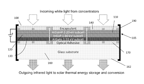
[0018] Figure IA shows one embodiment of a CPV module.
[0019] Figure IB shows a second embodiment of a CPV module.
[0020] Figure IC shows a third embodiment of a CPV module, wherein the said
module
comprises a transparent superstrate and transparent substrate, both comprised
of sapphire.
[0021] Figure 2 shows one embodiment of a CPV module comprising a number of
smaller multijunction PV cells mounted on glass substrate all supported on a
metal frame.
[0022] Figure 3 shows an exemplary CPV module, where said exemplary module
includes an array of sixteen (16) multijunction PV cells mounted on an infra-
red transparent
substrate, said cells being interconnected via interconnection lead; and
further shows the
fabrication of said subcells.
5a
Date Recue/Date Received 2021-11-10
CA 02953397 2016-12-21
WO 2015/200927 PCT/US2015/038396
[0023] Figure 4 shows a view of a sunlight concentration system, including
a perspective
view of a reflector, a closer view of a module, and a view of a module without
the transparent
superstrate which covers a CPV module.
[0024] Figure 5A shows positioning of an exemplary focal point module,
comprising a
CPV module and a thermal receiver relative to the focal point of an ideal
reflector.
[0025] Figure 5B shows positioning of a focal point module relative to the
focal point of
an exemplary non-ideal reflector.
[0026] Figure 6 shows three CPV modules with multijunction array elements,
where the
degree of shading is indicative of the relative temperate of each array
element.
[0027] Figure 7 shows the CPV modules shown in FIG. 6, but with light
intensity plots
replacing temperature plots.
[0028] Figure 8 shows two variations of a CPV module, each having 37
multijunction
array elements and 21 multijunction array elements, respectively.
[0029] Figure 9 shows the same modules as FIG. 8, but the light intensity
plots have been
replaced by temperature plots showing the relative temperature of each array
element.
[0030] Figure 10 shows three CPV modules, each having multijunction array
elements,
where the degree of shading is indicative of the relative temperate of each
array element.
[0031] Figure 11 shows changes in temperature recorded on individual
multijunction
array elements, and the changes in said temperatures caused by the removal of
select array
elements from the CPV module.
[0032] Figure 12 shows a CPV module comprised of twenty-one (21) array
elements,
where said array elements are connected to a system bus (not shown) via
interconnection leads.
6
CA 02953397 2016-12-21
WO 2015/200927 PCT/US2015/038396
[0033] Figure 13 shows a CPV module with an alternative arrangement of
array
elements, where said array elements are connected to a system bus (not shown)
via
interconnection (where interconnection is not representative of the exactly
manner of physically
connecting the array elements, but rather is representative of how said
elements are connected in
series).
[0034] Figure 14 shows a CPV module with an alternative arrangement of
array
elements, where said elements are separated into four groups, each of which
comprises a group
of eight (8) elements connected in series (as shown via the connecting lines
where each element
touched by a given line is connected in series with the other elements touched
by the same line),
and where groups are connected to one another in parallel.
[0035] Figure 15 shows a CPV module with another alternative arrangement of
array
elements, where said elements are separated into two groups, each of which
comprises a group of
eight (8) elements connected in series (as shown via the connecting lines,
where each element
touched by a given line is connected in series with the other elements touched
by the same line),
and where groups are connected to one another in parallel.
[0036] Figure 16 shows a graph of energy absorbed by a multijunction PV
cell with three
subcells, where band A, B, and C correspond to said three subcells and band D
corresponds to
energy transmitted to thermal receiver behind said PV cell.
[0037] Figure 17 shows the difference in light intensity between an array
of elements
where there is no focal point drift and an array of elements where there is
one degree of focal
point drift.
7
CA 02953397 2016-12-21
WO 2015/200927 PCT/US2015/038396
[0038] Figure 18 shows a CPV module which is "bifacial," which means that
the
interconnection leads are found on both the front and back of the PV module
(preferably in an
alignment so as to minimize shading by the interconnection leads).
[0039] Figure 19 shows a PSPICE model of an exemplary active control
circuit.
[0040] Figure 20 shows an embodiment of a system comprising a reflector, a
focal point
module, and support struts, and a stepper motor (with controller), where said
focal point module
is periodically realigned with the focal point of reflector by stepper motor.
[0041] Figure 21 shows an exemplary stepper motor assembly which comprises
x-axis
motor, threaded rod, y-axis motor, mounting rod, and CPV module.
DETAILED DESCRIPTION OF THE INVENTION
[0042] Detailed descriptions of one or more preferred embodiments are
provided herein.
It is to be understood, however, that the present invention may be embodied in
various forms.
Therefore, specific details disclosed herein are not to be interpreted as
limiting, but rather as a
basis for the claims and as a representative basis for teaching one skilled in
the art to employ the
present invention in any appropriate manner.
[0043] Wherever any of the phrases "for example," "such as," "including"
and the like
are used herein, the phrase "and without limitation" is understood to follow
unless explicitly
stated otherwise. Similarly "an example," "exemplary" and the like are
understood to be non-
limiting.
[0044] The term "substantially" allows for deviations from the descriptor
that do not
negatively impact the intended purpose. Descriptive terms are understood to be
modified by the
term "substantially" even if the word "substantially" is not explicitly
recited. Therefore, for
example, the phrase "wherein the lever extends vertically" means "wherein the
lever extends
8
CA 02953397 2016-12-21
WO 2015/200927 PCT/US2015/038396
substantially vertically" so long as a precise vertical arrangement is not
necessary for the lever to
perform its function.
[0045] The terms "comprising" and "including" and "having" and "involving"
(and
similarly "comprises", "includes," "has," and "involves") and the like are
used interchangeably
and have the same meaning. Specifically, each of the terms is defined
consistent with the
common United States patent law definition of "comprising" and is therefore
interpreted to be an
open term meaning "at least the following," and is also interpreted not to
exclude additional
features, limitations, aspects, etc. Thus, for example, "a process involving
steps a, b, and c"
means that the process includes at least steps a, b and c. Wherever the terms
"a" or "an" are
used, "one or more" is understood, unless such interpretation is nonsensical
in context.
[0046] For the purposes of this application, where the term "CPV module" is
used, unless
a specific reference number is used, such term refers equally to the general
category of "CPV
modules" described herein, including without limitation, CPV modules 100, 101,
103, 220, 310,
510, 1310, 1410, 1510, 1810, 2010 and 2118, or any other similar devices
described herein.
Moreover, the terms "CPV module" and "transmissive CPV module" are
interchangeable.
[0047] In one embodiment (not shown), the present invention provides a
multijunction
PV cell with at least two subcells of different bandgaps. Bandgaps for each
subcell may range
from about 1.4 eV to about 2.3 eV or may be outside this preferred range. In
another
embodiment, shown in FIG. IA, the CPV module 100 is comprised of multijunction
PV 105
which comprises three subcells 110, 120 and 130, with bandgaps of about 2.20
eV, about 1.80
eV and about 1.51 eV, respectively. FIG. 16 shows a graph of energy absorbed
by a
multijunction PV cell with three subcells (such as multijunction PV cell 105),
where bands A, B,
and C correspond to subcells 110, 120 and 130, respectively, and band D
corresponds to energy
9
CA 02953397 2016-12-21
WO 2015/200927 PCT/US2015/038396
transmitted to thermal receiver behind said CPV module 100. Each subcell 110,
120 and 130 is
constructed with type III-V materials, which are generally known as the
highest efficiency
materials used in PV cells. Alternatively, each subcell (making up PV cell
105) may be
constructed with any suitable material. In one embodiment, subcell 110 is
constructed from
AlGaInP, subcell 120 is constructed from InGaP, and subcell 130 is constructed
from AlGaAs.
In one embodiment, materials for each subcell are lattice-matched to gallium
arsenide or
germanium substrates. In other embodiments, materials for each subcell may be
lattice-
mismatched or metamorphic.
[0048] In some embodiments, the present invention includes one or more
encapsulant
materials 140 positioned above and/or below the multijunction PV 105 (see,
e.g., FIGS. 1A and
1B). In one embodiment, the one or more encapsulant materials are used in
tandem with an anti-
reflection coating, such as coatings 150a, 150b, 150c and 150d (collectively
referred to as anti-
reflection coating 150), where: 150a is applied at the junction between the
atmosphere and the
outer surface of superstrate 180; 150b is applied at the junction between
encapsulant 140 and PV
cell 105; 150c is applied at the junction between encapsulant 140 and
substrate 160; and, 150d is
applied at the junction between the atmosphere and the outer surface of
substrate 160. Exemplary
materials used for anti-reflection coating 150a include: (1) A1203 in a
thickness of 85 nm with
MgF2 in a thickness of 110 nm; (2) MgF2 in a thickness of 110 nm; and, (3)
A1203 in a
thickness of 85 nam with 5i02 in a thickness of 94 mn with MgF2 in a thickness
of 100 nm.
Exemplary materials used for anti-reflection coating 150b include: ZnS in a
thickness of 58 nm
with A1203 in a thickness of 85nm; (2) ZnS in a thickness of 58 nm with A1203
in a thickness of
100nm; and, (3) 5i02 in a thickness of 2 nm with ZnS in a thickness of 58 nm
with A1203 in a
thickness of 96 nm. Exemplary materials used for anti-reflection coating 150c
include: A1203 in
CA 02953397 2016-12-21
WO 2015/200927 PCT/US2015/038396
a thickness of 180 nm with ZnS in a thickness of 100 nm with MgF2 in a
thickness of 10 nm; (2)
A1203 in a thickness of 170 nm with ZnS in a thickness of 100 nm with MgF2 in
a thickness of
nm; and, (3) A1203 in a thickness of 154 nm with ZnS in a thickness of 109.
Exemplary
materials used for anti-reflection coating 150d include: (1) MgF2 in a
thickness of 190 nm; (2)
MgF2 in a thickness of 200 nm; and, (3) MgF2 in a thickness of 204 nm with
A1203 in a
thickness of 209 nm. The anti-reflection coating 150 is designed to provide
very low reflection
at each interface over a wide range of incident angles of incoming light, due
to the angle
dispersion of this incoming light from the concentrating optics, and over the
wavelength range of
the sun's spectrum incident on that interface. In some embodiments, the one or
more encapsulant
materials are comprised of silicone, or ethylene-vinyl (EVA), or any other
suitable material.
[0049] In some embodiments, the multijunction PV 105 cell is positioned on
a substrate
160. In one embodiment, substrate 160 comprises high infrared transparency
glass. In said
embodiment, the high infrared transparency glass substrate 160 demonstrates
high thermal
conductivity and mechanical stability. In some embodiments, the high
transparency glass may
transmit light in a wavelength range from about 400 nm to about 5 microns. In
other
embodiments, the high transparency glass may transmit light with at least a
range from about 800
nm to about 2.5 microns. As shown in FIG. 1B, substrate 160 may be formed of
any suitable
infrared-transparent substrate. For example, in some embodiments, the
substrate 160 may
comprise infrared-grade fused silica. In other embodiments, the substrate 160
may comprise
CaF2, MgF2, ZnSe, or any other suitable material. In one embodiment, the
substrate 160 may be
coated with anti-reflection coating 150 on either or both sides of the
substrate 160. In some
embodiments, the substrate 160 may be positioned within or on top of a
structural support frame
11
CA 02953397 2016-12-21
WO 2015/200927 PCT/US2015/038396
190. In one embodiment, the frame 190 is metal. In other embodiments, the
frame 190 may be
comprised of any suitable material.
[0050] In some embodiments, the multijunction PV cell 105 is secured to the
substrate
with an adhesive 170 (and, optical adhesive 170 can also be considered an
"encapsulant" as
discussed above). In an embodiment, the adhesive 170 comprises a transparent
liquid
photopolymer optical adhesive. In another embodiment, the optical adhesive 170
comprises a
mercapto-ester. In other embodiments, the adhesive 170 comprises chalcogenide
materials or any
other suitable materials with high transparency for out-of-band light, strong
and stable adhesion,
and high thermal conductivity. In some embodiments, the multijunction PV cell
105 is secured to
the substrate 160 via a direct wafer bond (not shown). In an exemplary
embodiment, an
intermediate optical anti-reflection coating 150 is applied to the
multijunction PV cell 105 to
work in tandem with the adhesive 170.
[0051] In an alternative embodiment, shown in FIG. 1B, the transmissive CPV
module
101 also includes an infrared-transparent superstrate 180. In another
alternative embodiment,
shown in FIG. IC, the transparent substrate 160 and the transparent
superstrate 180 are both
composed of sapphire. Said embodiment further includes heat sink fins 190
(shown in cross-
section; see FIG. 21 for an exemplary plan view) configured to be in contact
with the outer
circumference of the transmissive CPV module 103. The embodiment of FIG. 1C
further
comprises layers of optical adhesive 170. We speculate that a sapphire
superstrate 180 and/or
substrate 160 with a thickness in the range of 1 mm to 10 mm is best suited to
conduct heat away
from PV cell 105 to a heat sink, such as fins 190. In an embodiment, the fins
190 are comprised
of aluminum. In another embodiment, the fins 190 can be made of any suitable
heat-conducting
material.
12
CA 02953397 2016-12-21
WO 2015/200927 PCT/US2015/038396
[0052] In some embodiments, the CPV module may incorporate passive cooling,
with
PV cells (such as PV cells 350) spaced a sufficient distance apart such that
the substrate (such as
substrate 357) dissipates the heat generated in said PV cells 350 without an
active or power-
consuming cooling method. In other embodiments, the cooling mechanism may be
passively
integrated into the CPV module at the focal point of a CPV system (such as CPV
module 310) by
using highly thermally conductive superstrate and substrate materials (such as
sapphire) to
laterally extract heat to heat sinks attached on either side of the CPV module
310 (such as fins
190 shown in FIG. 1C and heat sink 2150 shown in FIG. 21). In some
embodiments, an
integrated active cooling system (not shown) may involve microfluidic heat
transport channels
that transport a cooling fluid directly behind metal busbars (such as busbars
240) to avoid light
absorption in the cooling fluid, or if the cooling fluid is a low light
absorption material, the
cooling may be integrated into the module between the multijunction PV cell
105 and the
substrate 160. In other embodiments, the cooling system may be directly
adjacent to the PV cell
105 on either side, where air, water, or another cooling fluid flows across or
next to all or part of
the surface of the CPV module (such as module 310) at a rate sufficient to
remove heat generated
in the CPV module.
[0053] In an embodiment, the contacts (such as contacts 390) on the
substrate side for
each subcell (such as subcells 371, 372 and 373) are recessed in each cell and
are planar with the
substrate (such as substrate 357). In another embodiment, the contacts (such
as contacts 390) are
not planar with the substrate (such as substrate 357). In some embodiments,
wire bonding (as
described below in connection with FIG. 3) is used to connect the subcells to
an electrical grid
printed on the substrate. In another embodiment, indium bump bonding (not
shown) is used to
connect subcells to the cell interconnection grid, or both indium bump bonding
and wire bonding
13
CA 02953397 2016-12-21
WO 2015/200927 PCT/US2015/038396
may be used in parallel, one for the top contacts and another for the bottom
contacts. However,
any suitable inter-connection method may be used to connect cells (such as
cells 350) together.
[0054] In FIG. 2 an embodiment of a transmissive CPV module 200 is shown
comprising
a number of smaller multijunction PV cells 210 mounted on glass substrate 260
(but any suitable
infra-red transparent substrate will do), all supported on metal frame 270. In
the embodiment of
FIG. 2, each smaller multijunction PV cell 210 is interconnected via
interconnection leads 220
such that moving along one side of the device CPV module 200, the voltage
produced from each
smaller multijunction PV cell 210 is added together while the currents match
(i.e., are similar in
value), and that moving along the adjacent side of the CPV module 200, the
voltages produced
from each smaller multijunction PV cell 210 match (i.e., are similar in value)
while the currents
are added together. In one embodiment, electrons generated in the
semiconductor material within
a given PV cell 210 travel to a number of collection fingers 230 to be
captured by the electrical
circuit. The collection fingers 230 may be comprised of narrow strips of metal
that are patterned
onto the surface of PV cell 210. The collection fingers 230 conduct current to
busbars 240, which
may consist of wider metal wires that then conduct the current to the
interconnection leads 220
between cells 210, where said busbars 240 are then connected to an
interconnection lead 220.
Each respective interconnect 220 is connected to contact pad 250, which is
itself connect to an
electrical system where the power generated by module 200 is either stored or
used.
[0055] In one embodiment, the smaller multijunction PV cells 210 are triple
junction
cells. In some embodiments, smaller multijunction PV cells 210 are arranged
such that the gap
290 between each cell is sufficient to transmit the full solar spectrum,
including in-band (i.e.,
light within the absorption band of the multijunction PV cells) and out-of-
band light (i.e., light
outside of the absorption band of the multijunction PV cells), through the
substrate 260 of the
14
CA 02953397 2016-12-21
WO 2015/200927 PCT/US2015/038396
device. This enables more light to be directed to a thermal receiver and
storage system (not
shown) mounted behind module 200 and enables easier dissipation of heat
generated in the cells
210. In other embodiments, the multijunction PV cells 210 are arranged such
that the gap 290
between each cell 210 is minimized so that minimal to no visible light can
pass through the
module 220 without first passing through one of the cells 210. We speculate
that an optical
bypass (OB) (i.e., the percentage of the surface area of a given CPV module
220 that is not
occupied by a multijunction PV cell 210) in the range of 30% to 50% is
preferred.
[0056] In some embodiments, such as that shown in FIG. 3, the CPV module
310 may be
placed at the focal point of a sunlight concentration system 300 to maximize
the amount of
concentrated sunlight entering the CPV module 310. In some embodiments, the
sunlight intensity
achieved in such a concentration system can reach from one-hundred to one-
thousand times
normal, unmagnified sunlight. In one embodiment, sunlight concentration system
300 comprises
a reflector 312, an actuator 315 (also commonly referred to as a solar
tracker), support struts 311,
and a focal point module 318, where said focal point module 318 further
comprises CPV module
310 and thermal receiver 320. As shown in FIG. 3, reflector 312 can be a
concentric (or
otherwise concave) reflector dish; additionally, in an alternative embodiment,
reflector 312 can
be replaced by a Fresnel lens concentrator (not shown). In an exemplary
embodiment, the focal
point module 318 is placed at the focal point of reflector 312 to maximize the
uniformity of
concentrated sunlight across the surface of CPV module 310. This may be
accomplished by
constructing CPV module 310 so that the area featuring PV cells 350 is smaller
than the focal
spot of the concentrated beam created by reflector 312, thus allowing light
around the edges of
the concentrated beam to bypass the multijunction PV cells 350 and to shine
directly into the
thermal receiver 320. In an alternative embodiment, the CPV module 310 may be
placed in the
CA 02953397 2016-12-21
WO 2015/200927 PCT/US2015/038396
path of a concentrated sunlight beam but not at the focal point of concentric
reflector 312, such
that a portion of the light bypasses the multijunction PV cells 350 around the
edges of same. This
placement enables the focal point of concentric reflector 312 to be at the
aperture of the thermal
receiver 320 and maximizes the uniformity of light on the CPV module, while
also minimizing
the aperture size of the thermal receiver 320. Maintaining uniformity of
illumination on the CPV
module 310 enables said module 310 to achieve maximum power output for a given
total
incident light intensity. Utilizing a placement as described herein
demonstrates an advantage of
the present invention relative to conventional CPV. In the present invention,
it is acceptable for
light to not be incident on the multijunction PV cells 350 as long as such
light is directed into the
thermal receiver 320. In conventional CPV systems, all concentrated sunlight
must be directed
onto the cells in the CPV module.
[0057] FIG. 3 also depicts an exemplary transmissive CPV module 310, where
said
exemplary module 310 includes an array of sixteen (16) multijunction PV cells
350 mounted on
an infrared transparent substrate 357, said cells 350 being interconnected via
interconnection
leads 360. As is discussed below, the CPV module 310 may be configured in many
different
ways by varying both the number of multijunction PV cells 350, the size of the
respective
multijunction PV cells 350, and the gaps 355 between the respective
multijunction PV cells 350.
FIG. 4 shows another view of system 300, including a perspective view of
reflector 312, a closer
(i.e., "exploded" or "zoomed in") view of module 318, and a second view of
module 318 without
the transparent sup erstrate which covers CPV module 310 (and, thus, showing
an exemplary
configuration of multijunction PV cells 350). Note that any infrared
transparent superstrate may
be used.
16
CA 02953397 2016-12-21
WO 2015/200927 PCT/US2015/038396
[0058] In some embodiments, the reflector 312 is not perfectly smooth or
uniform (and,
thus is not ideal). FIG. 5A shows positioning of an exemplary focal point
module 518,
comprising a CPV module 510 and a thermal receiver 520 relative to the focal
point of an ideal
reflector (not shown). FIG. 5B shows the positioning of the same focal point
module 518
relative to the focal point of an exemplary non-ideal reflector (not shown).
In both FIG. 5A and
5B, the lines passing through, and focusing on (or near), the focal point
module 518 are
simulated ray trajectories of light reflected by the exemplary ideal and non-
ideal reflectors,
respectively.
[0059] In an exemplary embodiment, the present invention provides a method
of
converting some solar energy to electricity while transmitting other solar
energy to an energy
conversion and/or storage system. Referring to system 300 of FIG. 3, the
present invention
carries out the aforementioned mentioned method by directing solar energy to a
CPV module
310 including at least one PV cells 350 which comprises at least two subcells
(such as subcells
371 and 372), each with a distinct bandgap. The subcells 371 and 372 absorb
high energy light
and convert such high energy light to electricity. Low energy light is
transmitted through the
CPV module 310 to an energy conversion and/or storage system (such as thermal
receiver 320).
In some embodiments, the high energy light comprises light with wavelengths of
about 280 nm
to about 1800 nm (although most systems operate in the 280 nm to 900 nm
range). In some
embodiments, the low energy light comprises light with wavelengths of about
700 nm to about
3000 rim. In some embodiments, the CPV module 310 includes at least two
photovoltaic subcells
(such as subcells 371 and 372), each with a distinct bandgap, and in a
preferred embodiment, the
device comprises three photovoltaic subcell junctions (such as PV cell 350)
with respective
bandgaps of about 2.2 eV, about 1.8 eV and about 1.51 eV. A graphs showing the
various bands
17
CA 02953397 2016-12-21
WO 2015/200927 PCT/US2015/038396
of solar energy, and the methods of capture by an embodiment of the present
invention, is shown
in FIG. 16 (showing bands A, B and C, corresponding to the three junctions of
a PV cell 350 as
shown, for example, in FIG. 3, and showing a fourth band D of energy which
passes through the
PV cell 350 and continues on to a thermal receiver, such as thermal receiver
320). In a preferred
embodiment, the device operates at temperatures of about 110 degrees Celsius
or below.
[0060] Experimental
[0061] Fabrication
[0062] One embodiment of the transmissive CPV module (such as CPV module
310)
may be fabricated as follows. Multiple junction III-V photovoltaic
heterostructures are grown
from precursors such as solid or metal-organic column III and column V
materials epitaxially on
GaAs or Ge substrates using metal-organic chemical vapor deposition (MOCVD),
molecular
beam epitaxy (MBE), or related epitaxial growth techniques. These epitaxially
grown materials
are then processed into PV cells (such as cells 350). First, top metallic
contacts (such as contacts
390) are patterned on the surface of the epitaxial growth and the contact
layer material in the III-
V epitaxy is preferentially removed where there is no contact metallization
performed on the
epitaxial wafers; in some embodiments, this may require a thermal annealing
step to achieve low
contact resistance. Next, the cells (such as cells 350) are protected by a
photoresist or related
material, and the spaces between said cells are etched through to the GaAs
substrate underneath.
Then, the triple junction cell epitaxial material is removed from the GaAs or
Ge substrate via
epitaxial liftoff, using a black wax handle or other removable handle.
Epitaxial liftoff is
accomplished by etching through a release layer (e.g., AlAs) using a highly
selective etchant
such as hydrofluoric acid. The black wax handle is then removed (a GaAs,
glass, or similar
handle may also be used).
18
CA 02953397 2016-12-21
WO 2015/200927 PCT/US2015/038396
[0063] The opposing side of the photovoltaic cells 350 are then patterned
with a metallic
grid (such as contacts 390), again removing the contact epitaxial layer where
it is not needed and
annealing as necessary. Ideally, the front and back metallic grids on either
side of the cells (such
as busbars 240) are co-aligned to minimize shadowing of light passing through
said cells. An
intermediate optical anti-reflection coating (such as coating 150) is applied
to this side, which is
designed to work in tandem with an optical adhesive or encapsulant (see FIG.
lA or 1B). The
encapsulant (such as encapsulant 14) is used to attach the lifted off triple
junction cells (such as
PV cell 105) to a highly-infrared transparent substrate (such as substrate
160). The cells should
be aligned with an electrical interconnect circuit (such as interconnects 220)
on the substrate
(such as substrate 160). An indium bump bond, wire bond, or other method or
methods can be
used to electrically connect the cell to the interconnect circuit from both
the top and bottom
contacts. A top anti-reflection coating is applied to the exposed surface of
the CPV module (i.e.,
the surface not on the substrate). An anti-reflection coating may also be
applied to the backside
of the glass substrate. Each of these coatings may be applied in one or more
layers of optical
coating materials using materials such as TiO2, MgF2, SiO2, or any other
suitable materials. For
example, see discussion above regarding placement of anti-reflection coatings
150.
[0064] FIG. 3 shows two approaches to subcell fabrication in line with the
fabrication
process described above. In the first process 370, three junctions 371, 372
and 373 are grown on
a GaAs substrate 374 with bandgaps of approximately 2.2 eV, 1.8 eV, and 1.5 eV
(plus or minus
0.1 eV), respectively. These layers are grown on an epitaxial liftoff layer,
allowing the triple
junction CPV subcell 375 (comprised of junctions 371, 372 and 373) to be
removed from the
GaAs substrate 374 via epitaxial liftoff and subsequently fabricated into a
cell 350. This epitaxial
lift-off process reduces optical losses for the infrared out-of-band light
passing through the new
19
CA 02953397 2016-12-21
WO 2015/200927 PCT/US2015/038396
cell, and reduces cost by allowing the GaAs wafer to be reused. In the second
approach 380,
three junctions 381, 382, and 383, are grown on a GaAs substrate 384, with
bandgaps of
approximately 2.1eV, 1.7eV, and 1.4eV (plus or minus 0.1 eV), respectively.
These junctions are
not grown with an epitaxial liftoff layer, and subcells are formed that
include the triple junction
epitaxy and the wafer into the fabricated subcell. We speculate that this is
an easier, lower risk
fabrication process than is commonly used, and that said process still allows
almost as much out-
of-band infrared light to pass through the cell as in the first approach 370.
As noted above,
metallic contacts 390 are patterned onto the top and bottom surfaces of the
cell material during
their formation.
[0065] An array, such as array 385, is formed from a set of isolated cells
350, with
appropriate contacts between elements formed via metallic interconnects 360
patterned onto the
substrate. Bypass diodes (not shown) are integrated as necessary behind (or
near) the
photovoltaic cells 350 in order to minimize losses related to partial
shadowing of the module
310. Finally, the wiring is completed. An encapsulating layer (such as
encapsulant 140) is
deposited via spinning or another means onto the array of cells 350 mounted on
the substrate
357. An infrared transparent superstrate (such as superstrate 180) is then
attached to the top of
array 385. An anti-reflection coating 150 may also be applied to the backside
of the substrate
(see as surface 162) and/or to the topside of the superstrate (see surface
182). The array 385 is
then framed as necessary for integration into a larger energy conversion
system (for example, see
module 318, including CPV module 310, as shown FIG. 4). A heat sink may be
integrated into
the frame to extract heat form the superstrate (such as superstrate 18) and
substrate 357 and
reject said heat into the environment (see, e.g., heat sink 2150 shown in FIG.
21, or heat sink fins
190 in FIG. 1C). A profile of a completed CPV module comprising a single PV
cell 350 is
CA 02953397 2016-12-21
WO 2015/200927 PCT/US2015/038396
shown in Figures 1A, 1B and 1C. A top down view of exemplary CPV module arrays
are shown
in Figures 2, 3 and 4. The spaces 355 between cells can be very narrow to
maximize the fraction
of photons converted directly to electricity by the PV cells 350.
Alternatively, the spacing 355
between cells 350 can be much larger (e.g., spacing between cells 350 on the
order of 1/10th to
10x the size of the cells 350) in order to enable more sunlight to pass
through the module 310 to
a thermal storage device (such as thermal receiver 320). This alternative
configuration, with
more spacing between cells 350, provides several benefits, such as the ability
to more easily keep
the cells 350 from overheating. As discussed below, arrays such as array 385
may come in many
configurations.
[0066] FIG.
6 shows three CPV modules 610, 620 and 630, each comprising 37
multijunction PV array elements 650, where the degree of shading is indicative
of the relative
temperature of each array element. Module 610 is comprised of multijunction
array elements 25
2 =
mm size,
with gaps 615 between respective array elements of 0.5 mm. Module 620 is
comprised of multij unction array elements 25 mm2 in size, with gaps 625
between respective
array elements of 1 mm. Module 630 is comprised of multijunction array
elements 25 mm2 in
size, with gaps 635 between respective array elements of 1.5 mm. As can be
seen in FIG. 6, the
maximum temperature measured is inversely proportional to the size of the gaps
between array
elements. And, the associated amount of energy which bypasses the PV module is
directly
proportional. FIG. 7 shows the same CPV modules shown in FIG. 6, but with
light intensity
plots replacing temperature plots.
[0067] FIG.
8 shows two variations of a CPV module, modules 810 and 820, each having
37 multijunction array elements 850 and 21 multijunction array elements 850,
respectively. FIG.
8 shows the relative intensity of light striking each element 850 of modules
810 and 820. The
21
CA 02953397 2016-12-21
WO 2015/200927 PCT/US2015/038396
size of array elements 850 in both modules 810 and 820 is 25 mm2, and the gap
825 between the
array elements of modules 810 and 820 is 0.5 mm. In view of the results of the
light intensity
plots shown in FIG. 8, it is speculated that the amount of light striking the
outer-most elements
of 810 is much lower than the intensity striking the inner array elements, and
thus we speculate
that the outer-most elements are not worth the added cost and heating to the
system (and the
elimination of said outer-most elements thus results in a module identical to
module 820). Thus,
said outer-most elements 850 may be removed without a significant loss in
energy capture by the
21 element module 810 as compared to the 37 element module 820; and, thus, we
speculate this
will allow for a material decrease in production costs with only an
incremental decrease in power
generation. FIG. 9 shows the same CPV modules as FIG. 8, but the light
intensity plots have
been replaced by temperature plots showing the relative temperature of each
array element. As
can be seem, the elimination of the outer-cells reduces the maximum
temperature experienced by
the CPV module by five (5) degrees centigrade.
[0068] FIG. 10 shows three CPV modules, 1010, 1020 and 1030, each having 21
multijunction array elements 1050, where the degree of shading is indicative
of the relative
temperature of each array element. Module 1010 is comprised of multijunction
array elements
36 mm2 in size, with gaps 1015 between respective array elements of 0.5 mm.
Module 1020 is
comprised of multijunction array elements 49 mm2 in size, with gaps 1025
between respective
array elements of 0.5 mm. Module 1030 is comprised of multijunction array
elements 49 mm2 in
size, with gaps 1035 between respective array elements of 1.5 mm. As can be
seen in FIG. 10,
the maximum temperature measured is affected by both changes in element size
as well as
changes in the size of the gap between elements.
22
CA 02953397 2016-12-21
WO 2015/200927 PCT/US2015/038396
[0069] FIG. 11 shows changes in temperature recorded on individual multi
junction array
elements, and the changes in said temperatures caused by the removal of select
array elements
from the CPV module. CPV module 1110 is a 37 element array. CPV module 1150 is
a 32
element array. In our model, we found that removing the center array element
1112, along with
the outer-most elements at the "center" of each side of said array (shown as
elements 1115),
resulted in a reduction of peak temperature from 140 degrees Celsius to 110
degrees Celsius.
Additionally, we found that the intensity of light hitting the center array
element 1112 caused the
current generated by element 1112 to be higher than the current generated by
other elements in
the module, thus making it more difficult to match the current from element
1112 with the
current from the other array elements. Further, the configuration of module
1150 is generally
easier to wire together, as the 37 element array of module 1110 required array
elements to be
wired in such a manner as to make overcurrent conditions more likely along the
associated
interconnection leads. In an alternative embodiment (not shown), center
element 1112 is kept,
but is of a smaller size than (i.e., has a smaller surface area than) the
other elements in the array
(and, so, this smaller center element 1112 would generate current closer to
the current generated
by other elements in the array, despite the intensity of light striking said
center element).
[0070] FIG. 12 shows a CPV module 1200 comprised of twenty-one (21) array
elements
1210, where said array elements 1210 are connected to a system bus (not shown)
via
interconnection leads 1220. Also shown are exemplary values 1230 and 1235,
where the values
1230 (at the top of the notated array elements) represents the intensity of
light measured on said
array element as a multiple of ordinary direct sunlight, and the value 1235
(at the bottom of the
notated array elements) represents the temperature measured on said array
element in degrees
23
CA 02953397 2016-12-21
WO 2015/200927 PCT/US2015/038396
Celsius. The shading differences on the plot shown in FIG. 12 depict
variations in light
intensity.
[0071] FIG. 13 shows a CPV module 1310 with an alternative arrangement of
array
elements 1320, where said array elements are connected to a system bus (not
shown) via
interconnection 1330 (where interconnection is not representative of the
exactly manner of
physically connecting the array elements, but rather is representative of how
said elements are
connected in series). More specifically, interconnect 1330 comprises series
loop 1330a and
series loop 1330b, where loop 1330a and 1330b are connected in parallel with
one another. This
arrangement is designed to connect those array elements 1320 in series that
share a similar
current (due to their receipt of similar light intensity based on their
position on module 1310).
[0072] FIG. 14 shows a CPV module 1410 with another alternative arrangement
of array
elements 1420, where said elements are separated into four groups, 1421, 1422,
1423 and 1424,
each of which comprises a group of eight (8) elements 1420 connected in series
(as shown via
the connecting lines 1471, 1472, 1473 and 1474, where each element 1420
touched by a given
line is connected in series with the other elements 1420 touched by the same
line), and where
groups 1421, 1422, 1423, and 1424 are connected to one another in parallel.
[0073] FIG. 15 shows a CPV module 1510 with another alternative arrangement
of array
elements 1520, where said elements 1520 are separated into two groups, 1521
and 1522, each of
which comprises a group of eight (8) elements 1520 connected in series (as
shown via the
connecting lines 1571 and 1572, where each element 1520 touched by a given
line is connected
in series with the other elements 1520 touched by the same line), and where
groups 1521 and
1522 are connected to one another in parallel.
[0074] Current Matching and Focal Point Drift
24
CA 02953397 2016-12-21
WO 2015/200927 PCT/US2015/038396
[0075] One of the major challenges in designing compact CPV modules of the
type
described herein is to maintain current matching between array elements
connected in series.
Current matching is especially important in situations where the focal point
of a reflector that is
part of a sunlight concentration system (such as system 300) drifts, thereby
causing some PV cell
array elements in a series of connected array elements to receive less light
than other array
elements in that same series of connected array elements. For example, FIG. 17
shows the
difference in light intensity between an array of elements 1710 where there is
no focal point drift
and an array of elements 1720 where there is one degree of focal point drift.
As these plots make
clear, if the wiring scheme shown in FIG. 15 were used in a situation where
one degree of focal
point drift takes place, the individual array elements in group 1522 could
have significantly
different current outputs.
[0076] An embodiment designed to mitigate the problems caused by focal
point drift is
shown in FIG. 18. In this embodiment, the CPV module 1810 is "bifacial," which
means that the
interconnection leads 1820 are found on both the front and back of the PV
module (preferably in
an alignment so as to minimize shading by the interconnection leads). Note
that all of the CPV
module embodiments described herein are designed in this "bifacial" manner. By
connecting all
of the array elements 1830 electrically in parallel with one another, all
currents in each cell add
and issues related to current matching are minimized. We speculate the voltage
mismatch will
not be a problem, as voltages are expected to be nearly the same on all cells,
due to higher
temperatures (which decreases voltage) and higher illuminations (which
increases voltage)
occurring concurrently in the same cells as the focal spot wanders.
[0077] In an alternative embodiment designed to mitigate the problems
caused by focal
point drift, active circuit control is employed to "regroup" array elements
contained within a
CA 02953397 2016-12-21
WO 2015/200927 PCT/US2015/038396
given PV module in order to group cells with similar current outputs into
strings with similar
voltage and, thus, minimize current and voltage mismatch issues as the focal
spot wanders.
Specifically, the individual array elements cells are actively rewired into
new "groups" by an
array of MOSFET's (see MOSFET's 1931, 1932, 1933 and 1934) activated by an
embedded
microcontroller running a custom sorting and measuring program. A PSPICE model
of an
exemplary active control circuit is shown in FIG. 19. Circuit 1900, shown in
FIG. 19, comprises
a microcontroller with two connections (MCU1) and (MCU2) designed to control
switching
transistors 1910 and 1920. It should be recognized that circuit model 1900 may
be replaced by
any control circuit capable of reconfiguring (i.e., regrouping array elements
connected in series)
array elements based on the current outputs of each individual array element
in a PV module.
[0078] The following algorithm is an example of code used to run a
microcontroller as
described in the preceding paragraph (where the following code is modified
from native
microcontroller code to run in Java). In the context of the circuit diagram of
FIG. 19, the
microcontroller code below has a list of coordinates for each array element.
When the algorithm
is fed the coordinates of the focal point of the reflector (i.e., the "sun
spot") (which may be
determined via various methods), the algorithm sorts and ranks each array
element by its
proximity to the sun spot. The algorithm can also directly track photocurrent
generated in each
cell to determine the appropriate sorting and ranking of cells. The algorithm
then organizes the
array elements into 4 groups or strings (this number is flexible). Circuit
1900 comprises two
groups (i.e., circuit paths). The MOSFET transistors allow array elements to
be bypassed by
some paths and connected in series to others. When the algorithm sorts the
array elements into
their paths, the microcontroller will set the transistors appropriately so
that each array element is
26
CA 02953397 2016-12-21
WO 2015/200927 PCT/US2015/038396
bypassed by all but its assigned path. Paths are denoted by V1+ and V2+, while
the connections
to the microcontroller are labeled MCUl and MCU2. The exemplary code is as
follows:
[0079]
import processing.core.*;
import processing.data.*;
import processing.event.*;
import processing.opengl.*;
import java.util.HashMap;
import java.util.ArrayList;
import java.io.File;
import java.io.BufferedReader;
import java.io.PrintWriter;
import java.io.InputStream;
import java.io.OutputStream;
import java.io.I0Exception;
public class ActiveRewireSim_v2_1 extends PApplet {
PFont f;
int celICt = 24;//totla number of cells
int cellW = 6;//number of columns
int cellH = 4;//number of rows
int celIR = 40;//cell radius(only for simulation)
int []xCell = new int[cellCt];//x values of cells
int []yCell = new int[celICt];//y values
float []dCell = new float[cellCt];//distance to sun spot
float[][] distMat = new float[2][cellCt];
//combined distance and number assignment
public void setup(){
size(100*(cel1W+1),100*(cel1H+1));
background(0);
f = createFont("Serif',32,true);
for(int i = 1; i < (cel1W+1); i++){//create cells/coordinates
for(int j = 1;j < (cel1H+1); j++)
int cellPos = ((j-1)*cellW)+i-1;
xCell[cellPos] = 100*i;
yCell[cellPos] = 100*j;
27
CA 02953397 2016-12-21
WO 2015/200927 PCT/US2015/038396
public void draw(){
background(0);
textFont(f,20);
fill(255);
textAlign(CENTER, CENTER);
text("Color indicates current group. Red = HIGH, Black = LOW",width/2,20);
text("Mouse indicates center of illumination.",width/2,50);
text("Numbers are proximity ranking.",widthI2,height-40);
for(int i = 0; i < cellCt; i++){//calculate distance to sun spot
float xDiffS = sq(abs(xCell[i] - mouseX));
float yDiffS = sq(abs(yCell[i] - mouseY));
dCell[i] = sqrt(xDiffS + yDiffS);
for(int i = 0; i<cellCt; i++){//create record of distance
distMat[0][i] = dCell[i];
distMat[l][i] = i;
float[][] distSort = sortRowTop(distMat, celiCt);//sort by distance
for(int i = 0; i<cellCt; i++){//determine coloring/wiring
if(i < cellCt/4){
stroke(255);
fill(255,0,0);
cellR = 47;
else if(i < celICt/2){
stroke(255);
fill(255,150,0);
cellR = 37;
else if(i < 3*cellCt/4)1
stroke(255);
fill(200,200,0);
cellR = 32;
else{
stroke(255);
fill(25,10,0);
28
CA 02953397 2016-12-21
WO 2015/200927 PCT/US2015/038396
cellR = 27;
//Draws cells and colrs/sizes by proximity to sun spot
jut intTop = PApplet.parseInt(distSort[l][i]);
ellipse(xCell[intTop],yCell[intTop],cellR,cellR);
fill(255);
text(i+1,xCell[intTop] ,yCell[intTop]);
stroke(255,128,0);
fill(255,200,0);
ellipse(mouseX,mouseY,25,25);//Draw sun spot
[0080] In another alternative embodiment designed to mitigate the problems
caused by
focal point drift, a small, two-axis stepper motor could be placed between the
transmissive CPV
and the support struts such that said motor could automatically realign the
CPV module to keep
the focal point of the reflector centered on the CPV. FIG. 20 shows such an
embodiment, where
system 2000 comprises a reflector 2012, a focal point module 2018 (which
further comprises
CPV module 2010), support struts 2011, and a stepper motor (with controller)
2013, where said
focal point module is periodically realigned with the focal point of reflector
2012 by stepper
motor 2013.
[0081] FIG. 21 shows an exemplary stepper motor assembly 2100 (such as the
motor
assembly 2013 referenced above), which comprises x-axis motor 2110, threaded
rod 2120, y-axis
motor 2130, mounting rod 2140, and CPV module 2118. The embodiment of FIG. 21
further
comprises heat sink 2150. In operation, a controller will actuate x-axis motor
2110 and y-axis
motor 2120 in order to keep CPV module 2118 within the focal point of a
reflector (such as
reflector 2012). Specifically, threaded rod 2120 is threaded through and
affixed to y-axis motor
2130 such that, when x-axis motor 2110 operates, y-axis motor 2130, mounting
rod 2140 and
CPV module 2118 all move linearly in the x-axis synchronously with x-axis
motor 2110.
29
CA 02953397 2016-12-21
WO 2015/200927 PCT/US2015/038396
Likewise, mounting rod 2140 is affixed to y-axis motor 2130 and CPV module
2118 such that,
when y-axis 2130 operates, mounting rod 2140 rotates, thereby causing CPV
module 2118 to
move linearly in the y-axis. We speculate that motor assembly 2100, when
controlled by a
control system, will keep CPV module 2118 within the focal point of any
associated solar
concentrator optic (such as reflector 2012). In an embodiment, the control
system could use the
power out from the CPV module 2010 as the feedback mechanism to guide the real-
time
realignment of the CPV module 2010 according to focal spot drift, with a goal
of maximizing
power output from CPV module 2010.
[0082] Electrical and optical physics and losses
[0083] When a thin multijunction PV cell mounted on high infrared
transparent substrate
is positioned in the path of concentrated light, the PV cell absorbs all of
the high energy light
above the bandgap of the lowest bandgap subcell (the in-band light) and
transmits most of the
remaining low energy light (the out-of-band light) (see, e.g., graph in FIG.
16 depicting bands
absorbed by CPV cell layers). This design results in extremely high
efficiency, with as much as
about 60% of in-band light energy converted to electrical energy, and with a
pass-through optical
transmission of as much as about 82% of the out-of-band light to the thermal
receiver or heat
storage device.
[0084] A CPV module could utilize single junction cells, dual junction
cells, or triple
junction cells. Quadruple junction cells may also be possible. The CPV module
may utilize more
than four junctions, including both epitaxially grown multijunction cells and
multijunction cells
that stack non-epitaxial junctions together into a monolithically integrated
device stack (for
example, by wafer bonding). The determination of which type of cell to use
involves a complex
CA 02953397 2016-12-21
WO 2015/200927 PCT/US2015/038396
optimization that takes into consideration other system losses and the
performance and needs of a
thermal storage device and a system for deploying the stored thermal energy.
The use of
additional junctions in the cell minimizes thermalization in the CPV
converter.
[0085] III-V cell materials are well established as the highest-performing
solar cell
material, due to high material quality, direct bandgaps across the solar
spectrum, and high
external radiative efficiency (ERE). About 2.20 eV is a high yet realistic
target for a direct band-
gap I11-V material lattice-matched to GaAs. The nitride material system is
another option to
convert high energy photons efficiently, as nitrides can attain much higher
energy direct
bandgaps .
[0086] A 2.20 eV junction may be formed from AlGaInP lattice-matched to
GaAs. To
achieve proper current matching and utilize realistic GaAs lattice-matched
materials, the other
two junctions may be InGaP at 1.80eV and AlGaAs at 1.51 eV. The energy cut-off
at 1.51 eV
between light converted by the PV cell and light transmitted to a thermal
storage device is an
important parameter for system optimization. The expected out-of-band
transmission losses are
shown in Table 1. Figure 16 shows a graph of how the spectrum is split between
wavelengths
that are converted directly to electricity and wavelengths that are
transmitted through the CPV
device and into a thermal storage device. The split shown is a preferred split
for a triple junction
cell, but the split may be located differently within the spectrum for various
embodiments of the
present invention.
31
CA 02953397 2016-12-21
WO 2015/200927 PCT/US2015/038396
.Additiunal
ANiorption: in ow:valiant 2.0%
:Retlectica at surface :of (PV 2.5%
ReflectionfabsenTition. at front contact grid 4.0%
Free carrier :nbsorption cell 04%
Reflectiontabsorption at back contact grid 2.0%
Reflection at CIN-giaa., interface 3.0%
Optical adiatsive betwegn cell and glass .1.004;
(absorpCionattering)
Absorption in glass substrate .15%
Reflection at gIns.s-air interface 3.0%
Total nuns:mission of below 1.,51eV light 8.2%
Table 1. Out-of-band transmission losses
[0087] Assuming 500X concentration of light directed to the CPV, with 2.5%
of
incoming light reflected from the front of the cell:
For the 2.20 eV subcell (assuming 90% absorption and 0.1% ERE): P., = 6.79
W/cm2
For the 1.80 eV subcell (assuming 90% absorption and 10% ERE): P,,,õ =
5.29W/cm2
For the 1.51 eV subcell (assuming 90% absorption and 1% ERE): P,,,õ = 4.15
W/cm2
[0088] Total power from current-matched subcells: 16.23 * 0.975 = 15.82
W/cm2
[0089] Total power in the solar spectrum above 1.51 eV: Power>1.51eV =
26.41 W/cm2
[0090] Total in-band efficiency of triple junction cell for light above
1.51 eV:
CPVeff= 59.9%
[0091] These expected performance values are derived from detailed balance
calculations
derated using realistic external radiative efficiency (ERE) and percent
absorption values for each
bandgap. The targeted current density, voltage, and fill factor for each
subcell arc shown in Table
32
CA 02953397 2016-12-21
WO 2015/200927 PCT/US2015/038396
2a. Table 2b shows the same values for a dual junction cell using bandgaps
that are less risky,
demonstrating that a high in-band conversion efficiency of 57.1% is
attainable.
Table 2a: High risk triple junction subcell
Bandgap (ERE) Pmaõ [W/cm2] Jse [A/cm2] Voc [V] Fill Factor
2.22 eV (0.1%) 6.39 3.67 1.88 0.927
1.80 eV (10%) 5.35 3.67 1.59 0.917
1.50 eV (1%) 4.08 3.67 1.24 0.899
Total power in-band = 26.62 W/cm2 Efficiency = 59.4%
Table 2b: Medium risk dual junction subcell
Bandgap (ERE) Pmaõ [W/cm2] Js, [A/cm2] Vo, [V] Fill Factor
2.05 eV (0.1%) 7.87 4.96 1.72 0.923
1.585 eV (4%) 6.14 4.96 1.36 0.906
Total power in-band = 24.52 W/cm2 Efficiency = 57.1%
[0092] Temperature and cooling
[0093] At 500 suns, in-band (above 1.51 eV) incoming solar power density
is 26.41
W/cm2. If the PV cells are 59.9% efficient in-band, heat generated from in-
band light is 10.59
W/cm2. At 500 suns, out-of-band (below 1.51 eV) incoming solar power density
is 18.59 W/cm2.
If approximately 15% of this light is absorbed in the CPV device, heat
generated from out-of-
band light is 2.79 W/crn2. The total heat from inefficient
conversion/transmission of light is 13.38
W/cm2; for an 18 cm by 18 cm module with close packing of subcells, 4,335 W of
heat will be
generated in the CPV device. For ease of calculations, it is assumed that
approximately 5kWt of
heat needs to be removed in a 5kWe CPV device.
[0094] Air, water or other cooling systems may be used to dissipate the
resultant heat in
the CPV device. In one embodiment, an air cooling system may involve an air
curtain that
efficiently drives air over the CPV device through a linear array of small
high-intensity fans. In
other embodiments, integrated water cooling in the shadow of the subcell's
busbars may be used
33
CA 02953397 2016-12-21
WO 2015/200927 PCT/US2015/038396
so as not to obscure the transmission of infrared light through the CPV
device. As previously
described, a water curtain may be used if the cooling fluid has very low
absorption of out of band
light. If subcells are spaced sufficiently apart in the module and heat can be
dissipated in the
substrate, active cooling may not be necessary, and passive cooling will
suffice.
[0095] The transmissive CPV device operates at about 110 degrees Celsius or
below.
This is an important distinction from other technologies that couple CPV with
solar thermal
energy generation, where the excess heat generated by the CPV is directly
harvested, and the
CPV operates at much higher temperatures (e.g. 200 degrees Celsius or above),
or the thermal
energy generation is at much lower temperatures (e.g., 200 degrees Celsius or
below). The
present invention can attain temperatures approaching 600 degrees Celsius or
even higher in the
thermal storage medium. In those coupled thermal energy harvesting systems,
fluid is directed
near the CPV to extract heat directly into the thermal energy generation and
storage system. The
downside of this approach is that the CPV operates with significantly reduced
performance at
high temperatures, and the system is much less efficient than the system
proposed here. The
transmissive CPV of the present invention operates at about 110C or below and
is designed to
keep the CPV device thermally isolated from the thermal storage device, which
in turn can
operate at its preferred, much higher, temperatures for optimal thermal
storage and energy
conversion to electricity.
34