Note: Descriptions are shown in the official language in which they were submitted.
CA 02953759 2017-01-06
MULTI-LAYER FORMS AND METHODS
OF MANUFACTURING THE SAME
FIELD OF THE DISCLOSURE
[0001] This patent relates to multi-layer forms and, more specifically, to
multi-layer
forms and methods of producing the same.
BACKGROUND
[0002] Cards or tags may be produced for identification purposes.
BRIEF DESCRIPTION OF THE DRAWINGS
[0003] FIG. 1 depicts an example apparatus that can be used to produce the
example
multi-layer forms disclosed herein.
[0004] FIGS. 2 ¨ 12 depict an example multi-layer form at various stages of
an
example production process.
[0005] FIGS. 13 and 14 depict an example card and/or form in accordance
with the
teachings of this disclosure.
[0006] FIGS. 15 and 16 depict an example sponsorship tag and/or form in
accordance with the teachings of this disclosure.
[0007] FIGS. 17 and 18 depict an example ornament and/or form in accordance
with
the teachings of this disclosure.
[0008] FIGS. 19 and 20 depict an example luggage tag and/or form in
accordance
with the teachings of this disclosure.
[0009] FIGS. 21 and 22 depict an example card and key tag and/or form in
accordance with the teachings of this disclosure.
-1-
CA 02953759 2017-01-06
[0010] FIG. 23 is a flowchart representation of an example process, which
may be
implemented using machine readable instructions, to produce the example forms
of
FIGS. 2 ¨ 22.
[0011] FIG. 24 depicts an example apparatus that can be used to produce an
example
multi-layer forms disclosed herein.
[0012] FIGS. 25 ¨ 35 depict an example multi-layer form at various stages
of an
example production process.
[0013] FIG. 36 is a flowchart representation of an example process, which
may be
implemented using machine readable instructions, to produce the example forms
of
FIGS. 13 ¨ 22 and 25 ¨ 35.
[0014] FIG. 37 shows an example web that can be used to produce the example
multi-layer forms disclosed herein.
[0015] FIG. 38 is a block diagram of an example processor platform capable
of
executing the instructions to implement the flowcharts f FIGS. 23 and 36 to
implement
the apparatus of FIGS. 1 and 24.
DETAILED DESCRIPTION
[0016] Certain examples are shown in the above-identified figures and
described in
detail below. In describing these examples, like or identical reference
numbers are used
to identify the same or similar elements. The figures are not necessarily to
scale and
certain features and certain views of the figures may be shown exaggerated in
scale or in
schematic for clarity and/or conciseness. Additionally, several examples have
been
described throughout this specification. Any features from any example may be
included
with, a replacement for, or otherwise combined with other features from other
examples.
-2-
CA 02953759 2017-01-06
[0017] The examples disclosed herein relate to example forms (e.g.,
mailers,
sponsorship tags, ornaments, luggage tags, card and key tags and/or removable
inserts)
produced in an in-line process. In some examples, the forms are produced using
a multi-
ply paper card surrounded by and/or positioned between polystyrene (poly). One
or more
of the plies may be static and/or variably embossed and/or imaged (e.g.,
static and/or
variably imaged) to enable a single print run to produce custom and/or
different forms for
different customers, recipients, etc. In some examples, the forms may be
embossed
and/or imaged with a number, a recipient's name, a company's name, advertising
material and/or any other indicia. The embossed area may be ink tipped to
visually
differentiate the embossed area from the rest of the form.
[0018] In some examples, the forms are produced by mating paper web(s) and
polystyrene (poly) web(s) and cutting, creasing, scoring, folding and/or
gluing one or
more of the webs before and/or after the webs are mated. In some examples, the
paper
web is wider than the poly web. The paper web may be variably imaged on a
first side
and adhesive and/or paste may be applied to approximately one half of the
first side (e.g.,
over the imaging) to enable the poly web to be adhered to the first side of
the paper web
and for the poly web to cover half of the first side of the paper web (e.g.,
over the
imaging).
[0019] In some examples, the mated webs travel through an embosser (e.g.,
opposing
rollers) where a portion of the mated webs is embossed with, for example, a
number (e.g.,
static fictitious credit card numbers, a variable number), a company's name or
any other
indicia. In some examples, the embossed portion corresponds to the front of
the form
-3-
CA 02953759 2017-01-06
and/or to one half of the poly web. The embossed area may be ink tipped (e.g.,
U.V. ink
tipped) and cured.
[0020] In some examples, adhesive and/or paste is applied to approximately
one half
of a second side of the paper web and the webs are folded in half to couple
the second
side side of the paper substrate together. In some examples, adhesive and/or
paste is then
applied to approximately one half of the first side of the paper web (e.g.,
the half of the
first side without the poly) and the webs are folded in half such that the
first side of the
paper web is coupled together and the poly web forms the front and back
surfaces of the
form. In some examples, the folded webs are die cut to round the corners of
the form
and/or perforations are added to enable the form to be easily removed from a
waste
matrix. The completed forms may then be glued to a carrier and/or another web
and/or
packaged for shipment. The example form may be a card, a sponsorship and/or
luggage
tag, a card and key tag, an ornament, etc.
[0021] While the above-example describes the first substrate as being a
paper web
and the second substrate as being a poly web, the substrates may be any other
suitable
material such as, for example, a plastic and/or Polyethylene terephthalate
(PET) web and
a poly web. In such examples, the plastic web may include a plurality of tags
(e.g., RFID
tags) coupled thereto. Thus, the cards and/or forms produced may include an
internal tag
and/or intelligent functionality.
[0022] FIG. 1 represents an example apparatus 100 that can be used to
implement the
processes disclosed herein to produce the example cards, tags, forms, etc. In
some
examples, the apparatus 100 may be an in-line process and includes first,
second and
third substrate movers 102, 103, 104; an imager (e.g., a variable imager) 106;
gluers 108,
-4-
CA 02953759 2017-01-06
110, 112, 114; maters 116, 118; an embosser (e.g., a static embosser) 120; a
U.V. ink
tipper 122; a curer 124; folders 126, 128; and a cutter 130. While the
stations and/or
portions 102 ¨ 130 of the apparatus 100 are depicted in a particular order,
the stations
and/or portions 102 ¨ 130 may be arranged differently. While the apparatus 100
is
depicted as having the gluers 110, 112 being separate from the folders 126,
128, in other
examples, the gluer(s) and the folding station(s) may be combined.
[0023] In some examples, during operation, the first substrate mover 102
feeds one
or more pieces of first substrate and/or a web of first substrate 132 into the
apparatus 100.
In some examples, the imager 106 images a first side of the first substrate
132. The
images may include personal information (e.g., a name, an address, etc.),
brand-related
images and/or text, advertisement related images and/or text, instructional
images and/or
text, etc. However, in other examples, the apparatus 100 does not include the
imager 106
and, thus the first substrate 132 is imaged at a different location (e.g., the
first substrate
132 is pre-imaged) and/or the first substrate 132 is not imaged.
[0024] The first gluer 108 may apply glue to a first portion of the first
surface and the
mater 116 may mate the first surface portion with a second substrate 134 such
that the
first and second substrates 132, 134 are coupled. In some examples, the second
substrate
134 is fed to the mater 116 by the second substrate mover 103. In some
examples, the
first substrate 132 is paper, Polyethylene terephthalate (PET) and/or plastic
and the
second substrate 134 is poly and/or any other type of film. The embosser 120
receives
and embosses the mated webs of the substrates 132, 134. In some examples, the
embosser 120 is a static embosser that embosses a name, a number, etc. on the
mated
webs of the substrates 132, 134. However, in other examples, the embosser 120
is a
-5-
CA 02953759 2017-01-06
variable embosser. The U.V. ink tipper 122 may apply ink to the embossed area
and the
curer 124 may cure the ink. In some examples, ink tipping the embossed area
enables the
embossed area to be visually differentiated from the surrounding substrate.
[0025] The second gluer 110 may apply glue to a second surface of the first
substrate
132 and the first folder 126 may fold the first substrate 132 in half along a
first fold such
the second surface of the first substrate 132 is coupled together and the
second substrate
134 is on a first side of the fold (e.g., the first folder 126 folds the first
substrate 132 in
half along along the first fold where the first fold is adjacent an edge of
the second
substrate 134). The second gluer 112 may then apply glue to a second portion
of the first
surface of the first substrate 132 and the second folder 128 may fold the
substrates 132,
134 in half along a second fold line such that the first surface of the first
substrate 132 is
coupled together and the second substrate 134 forms outward facing surfaces of
the card,
tag and/or form being produced. In some examples, the second fold line may be
substantially parallel to the first fold line. As used herein, the phrase
substantially
parallel means between about ten degrees of parallel and/or accounts for
manufacturing
tolerances. In some examples, the second substrate 134 forms an exterior
surface (e.g., a
back surface, a front surface) and/or layers of the produced card, tag and/or
form and the
first substrate 132 forms interior surfaces and/or layers of the produced
card, tag and/or
form.
[0026] The cutter 130 may round the corners of the card, tag and/or form
being
produced, add one or more lines of weakness to the card, tag and/or form
and/or cut
and/or remove a waste matrix surrounding the card, tag and/or form being
produced. In
some examples, the gluer 114 may apply glue to a back surface of the completed
card, tag
-6-
CA 02953759 2017-01-06
and/or form (e.g., the smooth back surface opposite the embossed front
surface) and the
mater 118 may mate the completed card, tag and/or form with a third substrate
136. The
third substrate 136 may be a carrier web used to produce a mailer, a mailer
insert, a form,
etc.
[0027] FIGS. 2 ¨ 12 depict different views during a fabrication process to
produce an
example card 1200 in accordance with the teachings of this disclosure. FIG. 2
depicts
glue 202 applied to a first portion 203 of a first surface 204 of the first
substrate 132 and
the second substrate 134 about to be coupled to the first portion 203. FIG. 3
depicts the
first and second substrate 132, 134 after the first and second substrates 132,
134 are
coupled and/or mated and FIG. 4 shows the embosser 120 embossing part of the
first
portion 203 such that an embossed area 402 protrudes from the second substrate
134.
FIG. 5 shows the U.V. ink tipper 122 applying ink to the embossed area 402 to
enable the
embossed area 402 to be visually differentiated from the second substrate 134
surrounding the embossed area 402.
[0028] FIG. 6 shows glue 602 applied to a second surface 604 of the first
substrate
132 and the first substrate 132 being folded about a first fold 606 such that
the first
portion 203 of the first substrate 132 is coupled to a second portion 608 of
the first
substrate 132 and an indentation 610 formed by the embossed area 402 is
covered by the
second portion 608. FIG. 7 shows the first and second portions 203, 608
coupled
together and the embossed area 402.
[0029] FIG. 8 shows glue 802 applied to the second portion 608 of the first
surface
204 and the first and second substrates 132, 134 being folded about a second
fold 804
such that a first half 806 of the second portion 608 is coupled to a second
half 808 of the
-7-
CA 02953759 2017-01-06
second portion 608. FIG. 9 shows a first and/or non-embossed side 902 of a
form 904
and FIG. 10 shows a second and/or embossed side 1002 of the form 904 where the
form
904 is to be die-cut to form the card 1200. FIG. 11 shows a waste matrix 1102
that
surrounds the card 1200 prior to removal and FIG. 12 shows the card 1200
produced. As
shown in FIG. 12, the card 1200 has first, second, third and fourth internal
plies 1202,
1204, 1206, 1208 formed from the first substrate 132 and first and second
external plies
1210, 1212 formed from the second substrate 134. In other examples, the card
1200 may
have any number of internal plies and/or any number of external plies.
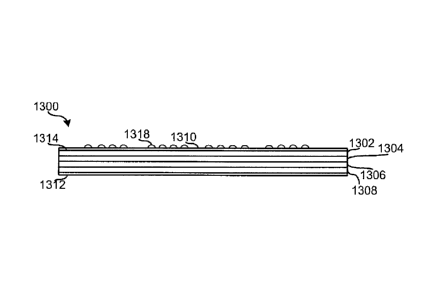
[0030] FIGS. 13 and 14 depict an example card and/or form 1300 in accordance
with the
teachings of this disclosure. In the illustrated example, the card 1300
includes first,
second, third and fourth paper plies 1302, 1304, 1306, 1308 positioned between
first and
second poly plies 1310, 1312. While the example card 1300 is described as
having four
paper plies and two poly plies, the example forms disclosed herein may have
any other
number of paper plies (e.g., 1, 2, 3, 5, etc.) and/or poly plies (e.g., 1, 3,
4, etc.).
[0031] As discussed above, the card 1300 is formed by mating the paper web
and/or the
first substrate 132 and the poly web and/or the second substrate 134 and
folding the
mated webs of the substrates 132, 134 such that the poly web and/or the second
substrate
134 forms the poly plies 1310, 1312 and the paper web and/or the first
substrate 132
forms the paper plies 1302, 1304, 1306, 1308. During the first folding process
performed
by the first folder 126, the first paper ply 1302 is coupled to the second
paper ply 1304
and the third paper ply 1306 is coupled to the fourth paper ply 1308. During
the second
folding process performed by the second folder 128, the second paper ply 1304
is
coupled to the third paper ply 1306.
-8-
CA 02953759 2017-01-06
[0032] As shown in FIGS. 13 and 14, a first surface 1314 of the first paper
ply 1302
includes imaging 1316 and the first paper and poly plies 1302, 1310 includes
an
embossed area 1318. Because the webs and/or the substrates 132, 134 are
embossed
prior to folding, no indentations are present on the second poly ply 1312. In
examples in
which the cards 1300 are packaged by stacking one card on top of the other,
the second
poly ply 1312 not having static embossing indentations prevents the cards 1300
from
sticking to one another and/or being coupled together. In some examples, not
having
indentations on the back surface of the card 1300 opposite the embossed front
surface
enables the back surface to relatively easily receive indicia, be printed on
and/or be
viewed after embossing the front surface.
[0033] FIGS. 15 and 16 depict an example card 1500 in accordance with the
teachings of
this disclosure. In the illustrated example, the card 1500 includes first,
second, third and
fourth paper plies 1502, 1504, 1506, 1508 positioned between first and second
poly plies
1510, 1512. In some examples, corners 1520, 1522, 1526, 1528 of the card 1500
are
formed by die cutting and perforations 1518, 1519 are added to the card 1500
to enable
an example sponsorship tag 1514 to be removed from a surrounding waste matrix
1516
and/or to define an aperture. As shown in FIG. 15, a first surface 1530 of the
first paper
ply 1502 includes imaging 1532 and the first paper and poly plies 1502, 1510
include an
embossed area 1534.
[0034] FIGS. 17 and 18 depict an example ornament and/or form 1700 in
accordance
with the teachings of this disclosure. In the illustrated example, the
ornament 1700
includes first, second, third and fourth paper plies 1702, 1704, 1706, 1708
positioned
between first and second poly plies 1710, 1712. In some examples, to enable
the
-9-
CA 02953759 2017-01-06
example ornament 1700 to be hung, a perforation 1714 is added to the ornament
1700 to
define a cutout 1715. In some examples, a perimeter surface 1716 is formed by
die
cutting. As shown in FIG. 17, a first surface 1718 of the first paper ply 1702
includes
imaging 1720 and the first paper and poly plies 1702, 1710 include an embossed
area
1722. In this example, the imaging 1720 identifies a family name and the
embossed area
1722 identifies a name of a company.
[0035] FIGS. 19 and 20 depict an example luggage tag and/or form 1900 in
accordance
with the teachings of this disclosure. In the illustrated example, the tag
1900 includes
first, second, third and fourth paper plies 1902, 1904, 1906, 1908 positioned
between first
and second poly plies 1910, 1912. In some examples, to enable the example tag
1900 to
be coupled to a piece of luggage, a perforation 1913 defines a cutout 1914.
[0036] As shown in FIG. 19, a first surface 1918 of the first paper ply 1902
includes
imaging 1920 and the first paper and poly plies 1902, 1910 include an embossed
area
1922. In this example, the imaging 1920 is used to include personal
information on the
tag (e.g., a person's name, etc.) and the embossed area 1922 identifies a name
of a
company.
[0037] FIGS. 21 and 22 depict an example card and/or form 2100 in accordance
with the
teachings of this disclosure. In the illustrated example, the form 2100
includes first,
second, third and fourth paper plies 2102, 2104, 2106, 2108 positioned between
first and
second poly plies 2110, 2112. In this example, the form 2100 includes a card
2114 and a
tag 2116. To enable the card 2114 and the tag 2116 to be removed from a
surrounding
waste matrix 2118, the form 2100 defines perforations 2120, 2122.
-10-
CA 02953759 2017-01-06
[0038] As shown in FIG. 21, a first surface 2124 of the first paper ply 2102
includes
imaging 2126, 2127 and the first paper and poly plies 2102, 2110 include an
embossed
area 2128, 2130. In this example, the imaging 2126, 2127 is used to include
personal
information on the form (e.g., a person's name, etc.) and/or a barcode and the
embossed
area 2128, 2130 identifies a name of a company.
[0039] FIG. 23
depicts an example flow diagram representative of a process that may
be implemented using, for example, computer readable instructions that may be
carried
out in conjunction with paper processing equipment such as die cutters, web
presses, etc.
to produce the forms disclosed herein and/or any other of the examples
disclosed herein.
The example processes of FIG. 23 may be performed using a processor, a
controller
and/or any other suitable processing device. For example, the example
processes of FIG.
23 may be implemented using coded instructions (e.g., computer readable
instructions)
stored on a tangible computer readable medium such as a flash memory, a read-
only
memory (ROM), and/or a random-access memory (RAM). As used herein, the term
tangible computer readable medium is expressly defined to include any type of
computer
readable storage and to exclude propagating signals. Additionally or
alternatively, the
example process of FIG. 23 may be implemented using coded instructions (e.g.,
computer
readable instructions) stored on a non-transitory computer readable medium
such as a
flash memory, a read-only memory (ROM), a random-access memory (RAM), a cache,
or any other storage media in which information is stored for any duration
(e.g., for
extended time periods, permanently, brief instances, for temporarily
buffering, and/or for
caching of the information). As used herein, the term non-transitory computer
readable
-11-
CA 02953759 2017-01-06
medium is expressly defined to include any type of computer readable medium
and to
exclude propagating signals.
[0040] Alternatively, some or all of the example processes of FIG. 23 may
be
implemented using any combination(s) of application specific integrated
circuit(s)
(ASIC(s)), programmable logic device(s) (PLD(s)), field programmable logic
device(s)
(FPLD(s)), discrete logic, hardware, firmware, etc. Also, some or all of the
example
processes of FIG. 23 may be implemented manually or as any combination(s) of
any of
the foregoing techniques, for example, any combination of firmware, software,
discrete
logic and/or hardware. Further, although the example processes of FIG. 23 are
described
with reference to the flow diagram of FIG. 23, other methods of implementing
the
processes of FIG. 23 may be employed. For example, the order of execution of
the
blocks may be changed, and/or some of the blocks described may be changed,
eliminated,
sub-divided, or combined. Additionally, any or all of the example processes of
FIG. 23
may be performed sequentially and/or in parallel by, for example, separate
processing
threads, processors, devices, discrete logic, circuits, etc.
[0041] FIG. 23 represents an example method of producing the examples
disclosed
herein. While the processes of the method are depicted as being performed
sequentially,
one or more of the processes may be performed in parallel, for example. The
process
may begin by unwinding a substrate and/or paper substrate from a roll and/or
moving one
or more pieces of the paper substrate into a press and toward an imager that
images the
paper substrate (blocks 2302, 2304). In some examples, the imager images a
portion of a
first side of the paper substrate. The images may include brand-related images
and/or
text, instructional images and/or text, personal information, a barcode, etc.
In some
-12-
CA 02953759 2017-01-06
examples, glue and/or paste may be applied to the imaged portion and/ the
first side of
the paper substrate and a poly web and/or substrate may be mated therewith
(blocks
2306, 2308). In some such examples, the poly substrate covers approximately
one half of
the paper substrate (e.g., over the glued portion) and the glue is
substantially clear when
dried.
[0042] In some examples, the mated substrates may pass through an embosser
that
embosses the mated substrates. (block 2310). The embosser may be a static
embosser
and/or a variable embosser that embosses a number(s), a name(s), etc. on a
portion of the
substrates. In some examples, the embossed area is ink tipped and cured.
(blocks 2312,
2314). The ink tipping enables the embossed area to stand out and/or be more
visible.
[0043] In some examples, paste and/or glue is applied to a second side of
the paper
substrate (e.g., opposite the side where the poly substrate is coupled) and
then the paper
substrate is folded in half such that the second side of the paper substrate
is coupled
together. (blocks 2316, 2318). In some examples, paste and/or glue is then
applied to the
first side of the paper substrate (e.g., the half of the first side not
covered by the poly
substrate) and then the paper and poly substrates are folded in half such that
the first side
of the paper substrate is coupled together and the poly substrate forms the
front and the
back of the form. (blocks 2320, 2322).
[0044] In some examples, to complete the process of producing the example
form, a
die cutter may cut the form from a surrounding matrix and/or produce one or
more lines
of weakness through the form. (block 2324). In some examples, the lines of
weakness
are perforations that define a cutout. The forms produced may then be mated
with
-13-
CA 02953759 2017-01-06
another web and/or carrier web using paste and/or glue (blocks 2326, 2328).
The carrier
web may be used to form a mailer, a mailer insert, a form, etc.
[0045] FIG. 24 represents an example apparatus 2400 that can be used to
implernent
the processes disclosed herein to produce the example cards, tags, forms, etc.
In some
examples, the apparatus 2400 may be an in-line process and includes first,
second and
third substrate movers 2402, 2404, 2406; an imager (e.g., a variable imager)
2408; an
embosser 2410; folders 2412, 2414; maters 2416, 2418; a fuser 2420; cutters
2421, 2422;
and a gluer 2424. While the stations and/or portions 2402 ¨ 2424 of the
apparatus 2400
are depicted in a particular order, the stations and/or portions 2402 ¨ 2424
may be
arranged differently and/or one or more of the stations and/or portions 2402 ¨
2424 may
be removed and/or combined.
[0046] In some examples, during operation, the first substrate mover 2402
feeds one
or more pieces of first substrate and/or a web of first substrate 2426 into
the apparatus
2400. In some examples, the first substrate 2426 is PET and/or any other
suitable type of
plastic that may or may not have intelligent inlays coupled thereto. In
examples in which
the first substrate 2426 includes inlays (e.g., RFID tags, NFC tags) coupled
thereto, the
cutter 2421 may die cut the first substrate to form a plurality of holes
and/or apertures
into which the chips of the inlays are to be positioned after the first
substrate 2426 is
folded during the production process to enable the form and/or card produced
to be
substantially flat, have a substantially consistent thickness and/or not have
a bulge
formed by the inlay. In some examples, the imager 2408 images a first side of
the first
substrate 2426. The images may include personal information (e.g., a name, an
address,
etc.), brand-related images and/or text, advertisement related images and/or
text,
-14-
CA 02953759 2017-01-06
instructional images and/or text, etc. However, in other examples, the
apparatus 2400
does not include the imager 2408 and, thus the first substrate 2426 is imaged
at a
different location (e.g., the first substrate 2426 is pre-imaged) and/or the
first substrate
2426 is not imaged.
[0047] The embosser 2410 receives and embosses the first substrate 2426. In
some
examples, the embosser 2410 is a static embosser that embosses a name, a
number, etc.
on the first substrate 2426. In other examples, the embosser 2410 is a
variable embosser
that embosses text (e.g., a person's name) and/or a variable number (e.g., a
credit card
number) on the first substrate 2426.
[0048] The first folder 2412 may fold the first substrate 2426 in half
along a first fold
such that a second surface of the first substrate 132 is immediately adjacent
each other.
The second folder 2414 may fold the first substrate 2426 in half along a
second fold line
such that the first surface of the first substrate 2426 is immediately
adjacent each other.
The mater 2416 may mate a second substrate (e.g., poly) 2428 with the opposing
exterior
surfaces of the folded first substrate 2426 and the fuser 2420 may fuse the
substrates
2426, 2428 together to form a card, tag and/or form. In some examples, the
fuser 2420
heat fuses and/or plastic welds the substrates 2426, 2428 together.
[0049] The cutter 2422 may round the corners of the card, tag and/or form
being
produced, add one or more lines of weakness to the card, tag and/or form
and/or cut
and/or remove a waste matrix surrounding the card, tag and/or form being
produced. In
some examples, the gluer 2424 may apply glue to a back surface of the
completed card,
tag and/or form (e.g., the smooth back surface opposite the embossed front
surface) and
the mater 2418 may mate the completed card, tag and/or form with a third
substrate 2430.
-15-
CA 02953759 2017-01-06
The third substrate 2430 may be a carrier web used to produce a mailer, a
mailer insert, a
form, etc.
[0050] FIGS. 25 ¨ 35 depict different views during a fabrication process to
produce
an example card 3500 in accordance with the teachings of this disclosure. FIG.
25
depicts the first substrate 2426 and FIG 26 shows the embosser 120 an embossed
area
2602 part of a first portion 2604 of the first substrate 2604 such that the
embossed area
2602 protrudes from a first side 2606 of the first substrate 2426.
[0051] FIG. 27 shows the first substrate 2426 being folded about a first
fold 2702
such that the first portion 2604 of the first substrate 2426 is adjacent to a
second portion
2704 of the first substrate 2426 and an indentation 2706 formed by the
embossed area
2602 is covered by the second portion 2704. FIG. 28 shows the first and second
portions
2604, 2704 immediately adjacent one another and the embossed area 2602.
[0052] FIG. 29 shows the first substrate 2426 being folded about a second
fold 2902
such that a first half 2904 of the second portion 2704 is adjacent a second
half 2906 of the
second portion 2704. FIG. 30 shows a first and/or non-embossed side 3002 of a
form
3004 and FIG. 31 shows a second and/or embossed side 3102 of the form 3004
where the
form 3004 is to be die-cut to form the card 3500. FIG. 32 shows a first
portion 3202 of
the second substrate 2428 coupled to the first and/or non-embossed side 3002
of the first
substrate 2426 and FIG. 33 shows a second portion 3302 of the second substrate
2428
coupled to the second and/or embossed side 3102 of the first substrate 2426.
[0053] FIG. 34 shows a waste matrix 3400 that surrounds the card 3500 prior
to
removal and FIG. 35 shows the card 3500 produced. As shown in FIG. 35, the
card 3500
has first, second, third and fourth internal plies 3502, 3504, 3506, 3508
formed from the
-16-
CA 02953759 2017-01-06
first substrate 2426 and first and second external plies 3510, 3512 formed
from the
second substrate 2428. In other examples, the card 3500 may have any number of
internal plies and/or any number of external plies. For example, in some
examples, the
card 3500 does not include the external 3510, 3512. In such examples, the card
3500 is
made of the first substrate 2426.
[0054]
FIG. 36 depicts an example flow diagram representative of a process that
may
be implemented using, for example, computer readable instructions that may be
carried
out in conjunction with paper processing equipment such as die cutters, web
presses, etc.
to produce the forms disclosed herein and/or any other of the examples
disclosed herein.
The example processes of FIG. 36 may be performed using a processor, a
controller
and/or any other suitable processing device. For example, the example
processes of FIG.
36 may be implemented using coded instructions (e.g., computer readable
instructions)
stored on a tangible computer readable medium such as a flash memory, a read-
only
memory (ROM), and/or a random-access memory (RAM). As used herein, the term
tangible computer readable medium is expressly defined to include any type of
computer
readable storage and to exclude propagating signals. Additionally or
alternatively, the
example process of FIG. 36 may be implemented using coded instructions (e.g.,
computer
readable instructions) stored on a non-transitory computer readable medium
such as a
flash memory, a read-only memory (ROM), a random-access memory (RAM), a cache,
or any other storage media in which information is stored for any duration
(e.g., for
extended time periods, permanently, brief instances, for temporarily
buffering, and/or for
caching of the information). As used herein, the term non-transitory computer
readable
-17-
.
CA 02953759 2017-01-06
medium is expressly defined to include any type of computer readable medium
and to
exclude propagating signals.
[0055] Alternatively, some or all of the example processes of FIG. 36 may
be
implemented using any combination(s) of application specific integrated
circuit(s)
(ASIC(s)), programmable logic device(s) (PLD(s)), field programmable logic
device(s)
(FPLD(s)), discrete logic, hardware, firmware, etc. Also, some or all of the
example
processes of FIG. 36 may be implemented manually or as any combination(s) of
any of
the foregoing techniques, for example, any combination of firmware, software,
discrete
logic and/or hardware. Further, although the example processes of FIG. 36 are
described
with reference to the flow diagram of FIG. 36, other methods of implementing
the
processes of FIG. 36 may be employed. For example, the order of execution of
the
blocks may be changed, and/or some of the blocks described may be changed,
eliminated,
sub-divided, or combined. Additionally, any or all of the example processes of
FIG. 36
may be performed sequentially ancUor in parallel by, for example, separate
processing
threads, processors, devices, discrete logic, circuits, etc.
[0056] FIG. 36 represents an example method of producing the examples
disclosed
herein. While the processes of the method are depicted as being performed
sequentially,
one or more of the processes may be performed in parallel, for example. The
process
may begin by unwinding a first substrate and/or plastic/PET substrate from a
roll and/or
moving one or more pieces of the plastic and/or PET substrate into a press and
toward a
cutter that forms chip receiving apertures in the first substrate and an
imager that images
the plastic substrate (blocks 3602, 3604). In some examples, the imager images
a portion
-18-
CA 02953759 2017-01-06
of a first side of the first substrate. The images may include brand-related
images and/or
text, instructional images and/or text, personal information, a barcode, etc.
[0057] In some examples, the first substrate passes through an embosser
that
embosses the first substrate. (block 3606). The embosser may be a static
embosser and/or
a variable embosser that embosses a number(s), a name(s), etc. on a portion of
the
substrate.
[0058] In some examples, the first substrate is folded in half such that
the second
side of the first substrate is immediately adjacent one another. (block 3608).
In some
examples, the first substrate is folded in half again such that the first side
of the first
substrate is immediately adjacent one another. (block 3610).
[0059] In some examples, the first substrate is mated with the second
substrate
and/or the poly web and the first and substrates are coupled together. (blocks
3612,
3614). In some examples, the second substrate includes a bar code, a magnetic
strip, etc.
to enable, for example, the card produced to be used as a credit card, an
access card, an
identification card and, more generally, to include and/or convey information.
In some
examples, the substrates are coupled together by fusing the layers of the
first substrate
together and/or fusing the first and second substrates together. In some
examples, to
complete the process of producing the form, a die cutter may cut the form from
a
surrounding matrix ancUor produce one or more lines of weakness through the
form.
(block 3616). In some examples, the lines of weakness are perforations that
define a
cutout. The forms produced may then be mated with another web and/or carrier
web
using paste and/or glue (blocks 3618, 3620). The carrier web may be used to
form a
mailer, a mailer insert, a form, etc.
-19-
CA 02953759 2017-01-06
[0060] FIG. 37 depicts an example substrate 3700 that can be used to
produce the
example card 3500. As shown, the substrate 3700 includes the fold lines 2702,
2902,
inlays 3'704 and apertures 3706. In practice, once the substrate 3700 is
folded about the
fold line 2702, chips 3708 of the inlays 3704 are received within the
apertures 3706 to
substantially ensure the card 3500 produced has a substantially consistent
thickness
and/or to substantially prevent the chips 3708 from being damaged (e.g., the
chips 3708
are substantially housed within the respective aperture 3706, thereby
protecting the chips
3708). In examples in which the chips 3708 are relatively thick and/or thicker
than the
substrate 3700, more than one aperture 3706 may be defied such that when the
substrate
3700 is folded about the fold line 2702, the respective chips 3708 are
received in two or
more apertures 3706.
[0061] FIG. 38 is a block diagram of an example processor platform 3800
capable of
executing the instructions of FIGS. 23, 36 to implement the apparatus 100 of
FIGS. 1, 24.
The processor platform 3800 can be, for example, a server or any other type of
computing device.
[0062] The processor platform 3800 of the illustrated example includes a
processor 3812.
The processor 3812 of the illustrated example is hardware. For example, the
processor
3812 can be implemented by one or more integrated circuits, logic circuits,
microprocessors or controllers from any desired family or manufacturer.
[0063] The processor 3812 of the illustrated example includes a local memory
3813 (e.g.,
a cache). The processor 3812 of the illustrated example is in communication
with a main
memory including a volatile memory 3814 and a non-volatile memory 3816 via a
bus
3818. The volatile memory 3814 may be implemented by Synchronous Dynamic
-20-
CA 02953759 2017-01-06
Random Access Memory (SDRAM), Dynamic Random Access Memory (DRAM),
RAMBUS Dynamic Random Access Memory (RDRAM) and/or any other type of
random access memory device. The non-volatile memory 3816 may be implemented
by
flash memory and/or any other desired type of memory device. Access to the
main
memory 3814, 3816 is controlled by a memory controller.
[0064] The processor platform 3800 of the illustrated example also includes an
interface
circuit 3820. The interface circuit 3820 may be implemented by any type of
interface
standard, such as an Ethernet interface, a universal serial bus (USB), and/or
a PCI express
interface.
[0065] In the illustrated example, one or more input devices 3822 are
connected to the
interface circuit 3820. The input device(s) 3822 permit a user to enter data
and
commands into the processor 3812. One or more output devices 3824 are also
connected
to the interface circuit 3820 of the illustrated example. The interface
circuit 3820 of the
illustrated example, thus, typically includes a graphics driver card.
[0066] The interface circuit 3820 of the illustrated example also includes a
communication device such as a transmitter, a receiver, a transceiver, a modem
and/or
network interface card to facilitate exchange of data with external machines
(e.g.,
computing devices of any kind) via a network 3826 (e.g., an Ethernet
connection, a
digital subscriber line (DSL), a telephone line, coaxial cable, a cellular
telephone system,
etc.).
[0067] The processor platform 3800 of the illustrated example also includes
one or more
mass storage devices 3828 for storing software and/or data. Examples of such
mass
-21-
CA 02953759 2017-01-06
storage devices 3828 include floppy disk drives, hard drive disks, compact
disk drives,
Blu-ray disk drives, RAID systems, and digital versatile disk (DVD) drives.
[0068] The coded instructions 3832 of FIGS. 23, 36 may be stored in the mass
storage
device 3828, in the volatile memory 3814, in the non-volatile memory 3816,
and/or on a
removable tangible computer readable storage medium such as a CD or DVD.
[0069] From the foregoing, it will appreciated that the above disclosed
methods,
apparatus and articles of manufacture relate to forms and/or forms produced in
an in-line
process. In some examples, the example forms are produced using a roll of
paper that is
folded and/or glued one or more times. In other examples, the example forms
are
produced using a roll of plastic (e.g., PET, plastic film) that is folded
and/or fused one or
more time times. In example in which the forms are produced using plastic, an
inlay
and/or tag (e.g., and RFID inlay, an NFC inlay) may be internally positioned
within the
card produced and/or positioned on and/or carried by the plastic web. Making
intelligent
cards (e.g., cards including RFID and/or NFC inlays) using an in-line process
may
significantly reduce the cost of producing such cards.
[0070] In examples in which the example plastic cards are produced without an
embedded tag, the example cards may be produced by using a roll of film
material that is
folded and/or fused. In some such examples, the film is a white material
and/or imaged
with digital, flexographic, offset and/or other static and/or variable
printing technologies.
In some examples, an exterior layer of film (e.g., poly film) may be coupled
and/or fused
to the folded PET layers to substantially protect the imaged data, for
example.
[0071] In examples in which the plastic cards are produced with an embedded
tag and/or
intelligent functionality (e.g., RFID tag, NFC tag and/or another functional
-22-
CA 02953759 2017-01-06
I
component(s)), the example cards are produced with a roll of film having
inlays ancUor
tags positioned thereon where the film is folded and/or fused. In some
examples, the
inlays and/or tags are positioned on the PET film by printing and/or imaging
an antenna
on the film and then positioning a chip adjacent the antenna. In some
examples, to
substantially prevent deformation and/or damage of the card including the
intelligent
functionality (e.g., RFID tag, NFC tag), the PET film may be die cut to form
an aperture
into the chip of the tag is received after the PET film is folded.
[0072] Although certain example methods, apparatus and articles of
manufacture
have been described herein, the scope of coverage of this patent is not
limited thereto.
On the contrary, this patent covers all methods, apparatus and articles of
manufacture
fairly falling within the scope of the claims of this patent.
-23-