Note: Descriptions are shown in the official language in which they were submitted.
CA 02954593 2017-01-09
WO 2016/005925
PCT/1B2015/055178
1
DEVICE FOR HARVESTING DIRECT LIGHT AND DIFFUSE LIGHT
FROM A LIGHT SOURCE
CRO S S -REFERENCE
[01] The present application claims the benefit of and priority to United
States Provisional
Patent Application Serial No. 62/022,078, filed July 8, 2014, entitled "Device
for Harvesting
Direct Light and Diffuse Light from a Light Source"; the contents of which are
incorporated
herein by reference in their entirety for all purposes.
FIELD
[02] The present technology relates to devices for harvesting direct light and
diffuse light
from a light source.
BACKGROUND
[03] For many reasons, there has been a growth in the development of
technologies used to
harness renewable sources of energy as an alterative to the generation of
energy via
combustion of hydrocarbons. One such renewable source of energy that has seen
some
attention is solar energy.
[04] Devices used to harvest solar energy have been known in the art for some
time. The
most common of such devices are relatively large flat-panel solar panel
assemblies. Such
solar panels typically comprise a series of flat "single-junction" crystalline
silicon
photovoltaic cells that are mechanically and electrically connected together
to form a large
panel assembly. That panel assembly is then mounted on a supporting structure.
Light
impinging on the panel assembly enters the photovoltaic cells for harvesting
thereby. Solar
panel assemblies of this type have been used for some time and remain in use
today.
[05] Such solar panel assembles are not suitable for use in many instances
owing to the
fact that the efficiency of the photovoltaic cells thereof in converting
sunlight into electrical
energy is relatively low. Thus, in some instances, only a small amount of
usable electrical
energy would be generated, which would not be sufficient to meet the
electrical requirements
of the particular intended application. In other instances, a large number of
such solar panel
assemblies would be required to generate a particular desired amount of
electricity, rendering
CA 02954593 2017-01-09
WO 2016/005925
PCT/1B2015/055178
2
such electricity more expensive to generate than via another method of
electrical power
generation.
[06] To attempt to overcome this difficulty, high-efficiency photovoltaic
cells ("RE-PV
cells") (e.g. triple junction cells) were developed. As their name suggests,
such RE-PV cells
are materially more efficient at converting sunlight into electrical energy
than are the
conventional single-junction photovoltaic cells referred to above. The RE-PV
cells are also,
however, significantly more expensive to manufacture than conventional single-
junction
photovoltaic cells. So much so that in order to for it to be economically
feasible to use such
RE-PV cells in a solar electricity generation application where cost is an
issue (which is most
applications), only an RE-PV cell of a very small size (relative to the
conventional single-
junction crystalline silicon photovoltaic cells found in the large flat-panel
solar panel
assemblies referred to above) can be used.
[07] This situation has generated an interest in concentrated photovoltaic
(CPV) systems.
The theory behind a CPV system is to use optical elements to concentrate
sunlight received
over a relatively larger area into a relatively smaller area of an RE-PV cell.
Since such
optical elements are relatively inexpensive, in theory, their combination with
an HE-PV cell
of a relatively small size would make solar energy generated by such systems
economically
feasible. (A cost comparison might be made, for example, between the cost of a
standard
conventional flat-panel solar panel assembly of a given area and a CPV system
having a light
acceptance area of the same given area.)
[08] There is an important drawback of CPV systems. The optical elements used
to
concentrate the light impinging on the system have a very small acceptance
angle for any
incoming light. (Generally, only light within that acceptance angle is
accepted by the system
for concentration and ultimate harvesting, all other light is generally not
harvestable by the
system.) This means that in most CPV systems, generally only direct normal
light (typically
referred to in the art as direct normal irradiance (DNI)) is accepted by the
optical elements
thereof and is harvestable by the system. Since the sun moves across the sky
during the day,
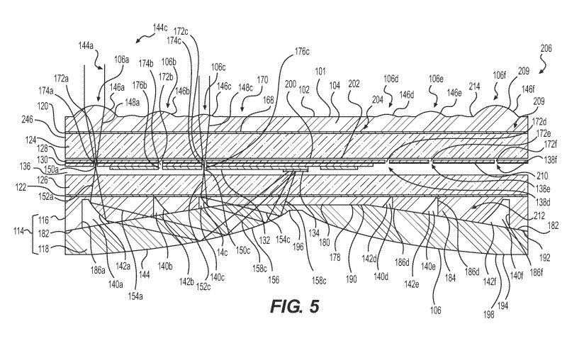
it is not economically feasible to stationarily mount a CPV system on a
support structure.
Typically, such a system is mounted with a two-axis "tracker", which is a
mechanism that
reorients the system throughout the day to maintain the entrance of light to
the optical
elements normal to the sun into order to maximize the amount of DNI that the
system
receives.
CA 02954593 2017-01-09
WO 2016/005925
PCT/1B2015/055178
3
[09] However, not all of the total light received from the sun at a particular
location on the
Earth by a panel on a tracker (known in the art as global normal irradiance
(GNI)) is DNI.
Molecules and suspensoids in the Earth's atmosphere will scatter some of the
beam of light
incoming from the sun to produce what is known in the art as "diffuse light"
(i.e. non-direct
light in that particular situation). The ratio of DNI to GNI (i.e. how much of
the sunlight at a
particular location is direct normal sunlight that has not been scattered)
varies by location on
the Earth and with time. For example, the ratio will be affected by then
current
meteorological conditions at the location on the Earth receiving the sunlight.
On an overcast
day in Toronto for example, the ratio is zero as all of the light is diffuse
sunlight. On a clear
sunny winter day in Toronto, approximately 85% of the sunlight received is DNI
(owing to
the relative lack of moisture and smog in the air); whereas on a clear sunny
summer day in
Toronto, approximately 70% of the sunlight received is DNI (owing to the
greater presence
of moisture and smog in the air).
[10] As was discussed above because of their optical elements' small
acceptance angles,
conventional CPV systems are generally incapable of harvesting diffuse light.
Diffuse light
is simply lost to a conventional CPV system, which offsets in part the
efficiency gains with
respect to the harvesting of direct sunlight in such systems. This also means
that even with a
tracker there is a portion of the GNI that is inaccessible by the system. For
any particular
location on the Earth an average annual DNI and DNI to GNI ratio can be
calculated in order
to evaluate the economics of the installation of a conventional CPV system.
[11] In order to potentially improve the economics of a conventional CPV
system, systems
have been proposed in which some diffuse light may also be accepted and
harvested by the
system. In this respect, various "hybrid" systems, being combination of a non-
concentrated
photovoltaic system with concentrated photovoltaic system have been proposed.
[12] One such hybrid system is described in U.S. Patent Application
Publication No. US
2010/0126556 Al, published May 27, 2010, entitled "Photovoltaic Concentrator
with
Auxiliary Cells Collecting Diffuse Radiation"; the abstract of which provides:
"High-
concentration photovoltaic concentrators can utilize much more expensive high-
efficiency
cells because they need so much less of them, but much of the solar resource
is left
ungathered thereby. The main cell is at the focal spot of the concentrator.
Low-cost
secondary solar cells are now added to the concentrator, surrounding the main
cell. Diffuse
skylight and misdirected normal rays irradiate these secondary cells, adding
to output. Also,
CA 02954593 2017-01-09
WO 2016/005925
PCT/1B2015/055178
4
the power plant can have output on cloudy days, unlike conventional
concentrators. As cell
costs fall relative to other costs, this system becomes economically superior
to both flat-plate
and concentrator systems."
[13] Another such hybrid system is described in U.S. Patent Application
Publication No.
US 2012/0255594 Al, published October 11, 2012, entitled "Solar Power
Generator
Module"; the abstract of which provides: "A solar power generator module
includes a first
type of photovoltaic cell and a second type of photovoltaic cell. The second
type of
photovoltaic cell is different from the first type of photovoltaic cell. The
module further
includes an optical device adapted to concentrate light onto the first type of
photovoltaic cell
and to transmit diffused light to the second type of photovoltaic cell."
[14] While hybrid systems such as those described in the '556 Publication
and the '594
Publication may be useful, improvements in such hybrid systems are nonetheless
possible.
SUMMARY
[15] It is an object of the present technology to provide an improved device
for harvesting
both direct and diffuse light as compared with at least some of the prior art.
[16] It is another object of the present technology to provide a hybrid device
for harvesting
sunlight that combines a concentrating photovoltaic system for harvesting
direct sunlight and
a non-concentrating photovoltaic system for harvesting diffuse sunlight.
[17] In one of its simplest forms the present technology provides a solar
panel device
having a concentrating aspect and non-concentrating aspect. (It should be
understood that the
description of this extremely simple embodiment which follows is not intended
to be a
definition of the present technology, but simply an aid to understanding the
present
technology. Embodiments which are far more complex are within the scope of the
present
technology, and are described in the paragraphs that follow the present
paragraph.) In this
simple embodiment, the non-concentrating aspect uses a solar panel similar to
a conventional
non-concentrating solar panel but having a series of holes in some of the
panel's non-
transparent components. The concentrating aspect uses this solar panel as a
support for a
series of lenses located on top of the panel and a series of reflectors
located on the bottom of
the panel. Direct sunlight is focused by the lenses through the holes to the
reflectors, which
then reflect the light to a high efficiency solar cell for harvesting. Thus,
the direct sunlight is
CA 02954593 2017-01-09
WO 2016/005925
PCT/1B2015/055178
harvested by the device as if the device were a concentrated photovoltaic
solar device alone.
Diffuse sunlight travels through the concentrating elements to the solar panel
for harvesting.
Thus, the diffuse light is harvested by the device as if the device were a
conventional solar
panel alone.
5 [18] Turning now to consider other embodiments, in more general terms,
embodiments of
the present technology provide a device for harvesting direct light and
diffuse light from a
light source, the device comprising: (I) A first photovoltaic cell. The first
photovoltaic cell
has an upper surface, a lower surface, and an array of optical passages
therein in optical
communication with the upper surface and the lower surface. (II) An array of
optical
concentrating elements is above the upper surface of the first photovoltaic
cell and defines a
light acceptance area. Each of the optical concentrating elements is
associated with one of
the optical passages. Each of the optical concentrating elements is structured
and arranged to
concentrate direct light from the light source impinging on that optical
concentrating element
towards the one of the optical passages associated with that optical
concentrating element.
The concentrated direct light passes through the first photovoltaic cell via
the optical passage
and exits the first photovoltaic cell via the lower surface as a non-parallel
beam of light.
Diffuse light from the light source passes through the array of optical
concentrating elements
to the upper surface of the first photovoltaic cell and enters the first
photovoltaic cell for
harvesting thereby. (III) An array of optical redirecting elements is below
the lower surface
of the first photovoltaic cell. Each of the redirecting elements is associated
with one of the
optical passages. Each of the redirecting elements receives the beam of light
from the optical
passage with which that redirecting element is associated and redirects the
beam of light
optically towards a second photovoltaic cell for harvesting thereby. The
second photovoltaic
cell has an active area receiving the beams of the light. The active area of
the second
photovoltaic cell is smaller than the light acceptance area defined by the
array of optical
concentrating elements by a concentration factor.
[19] The first photovoltaic cell has an upper surface, a lower surface, and an
array of
optical passages therein in optical communication with the upper surface and
the lower
surface. In the context of the present disclosure, the expression "optical
passages" should be
understood as including any structure or combination of structures that allows
light to pass
through that which the optical passage traverses, e.g. the first photovoltaic
cell. No particular
structure (other than that necessary to accomplish the aforementioned
function) is required.
CA 02954593 2017-01-09
WO 2016/005925
PCT/1B2015/055178
6
Non-limiting examples of optical passages are openings, holes, light pipes, or
transparent
materials that are appropriately structured and arranged with respect to the
light in question.
Thus, in the present disclosure, the expression an "array of optical passages
therein in optical
communication with the upper surface and the lower surface" should be
understood as any
series of structures that allow light to pass from the upper surface of the
first photovoltaic cell
through the first photovoltaic cell and to exit from the lower surface of the
first photovoltaic
cell. The use of the word "array" in this context should not be understood to
require a
particular ordering or grouping of the optical passages or some portion of the
optical
passages. Further, each of the optical passages in the array may be identical
to the others,
although they need not be.
[20] The type, structure, method of manufacturing, and/or principle of
operation of an
optical passage may be a function of the type, structure, method of
manufacturing and/or
principle of operation of the first photovoltaic cell (although it may not
be). In a non-limiting
example, in the case where the first photovoltaic cell is a single-junction
crystalline silicon
flat-panel structure, the optical passages therein may be holes that have been
laser drilled
therein.
[21] An array of optical concentrating elements is above the upper surface of
the first
photovoltaic cell defining a light acceptance area. In the context of the
present disclosure, the
expression "optical concentrating element" should be understood as including
any structure
that concentrates light passing through it. Thus, non-limiting examples of
optical
concentrating elements include lenses, Fresnel lenses, Winston cones, etc. It
is not necessary
that an optical concentrating element concentrate all of the light that passes
through it. It is
sufficient that a majority of light passing through a structure be
concentrated in order for the
structure to be considered an optical concentrating element.
[22] In some embodiments, optical concentrating elements serve the sole
function of
concentrating the light impinging upon them. In other embodiments, optical
concentrating
elements serve an additional function with respect to the light. As a non-
limiting example,
optical concentrating elements may also change the direction of the light
impinging on them
(e.g. focus the light). In some embodiments, some of the optical concentrating
elements have
the sole function of concentrating the light impinging on them, while other
optical
concentrating elements have an additional function(s) with respect to the
light. In some
embodiments, the additional function(s) are the same as between optical
concentrating
CA 02954593 2017-01-09
WO 2016/005925
PCT/1B2015/055178
7
elements (that have an additional function(s)), while in other embodiments,
the additional
function(s) differ between optical concentrating elements (that have an
additional
function(s)).
[23] The use of the word "array" in this context should not be understood to
require a
particular ordering or grouping of the optical concentrating elements or some
portion of the
optical concentrating elements. In some embodiments, the optical concentrating
elements of
the array of optical concentrating elements are all of the same design. In
other embodiments,
various optical concentrating elements of the array of optical elements are of
different
designs. The optical concentrating elements being "above the upper surface of
the first
photovoltaic cell", includes both structures where the optical concentrating
elements are in
direct physical contact with the upper surface of the first photovoltaic cell
and those where
the optical concentrating elements are not direct in physical contact with the
upper surface of
the first photovoltaic cell (e.g. structures wherein the optical concentrating
elements are
spaced apart from the upper surface of the first photovoltaic cell).
[24] The array of optical concentrating elements defines a "light acceptance
area" of the
device. In this respect, each of the optical concentrating elements has a
certain cross-
sectional area (in a plane normal to the incoming direct light) through which
the incoming
light can enter that optical concentrating element. The totality of these
areas of each of the
optical concentrating elements is the light acceptance area of the array.
[25] Each of the optical concentrating elements is associated with one of the
optical
passages. Thus, an optical concentrating element may be associated with a
single one of the
optical passages. In such a case, all of the light from that optical
concentrating element that
enters an optical passage enters a single optical passage (although it may be
some of the light
from that one of the optical concentrating elements enters no optical passage
at all).
Alternatively, an optical concentrating element may be associated with more
than one of the
optical passages. In such a case, the light from that optical concentrating
element that enters
an optical passage enters more than one optical passage (although, again, it
may be that some
of the light from that one of the optical concentrating elements enters no
optical passage at
all). Thus, in some embodiments, each of the optical concentrating elements is
associated
with a single optical passage. In other embodiments, each of the optical
concentrating
elements is associated with multiple optical passages. In still other
embodiments, some of
CA 02954593 2017-01-09
WO 2016/005925
PCT/1B2015/055178
8
the optical concentrating elements are associated within a single optical
passage while others
of the optical concentrating elements are associated with multiple optical
passages.
[26] Each of the optical concentrating elements is structured and arranged to
concentrate
direct light from the light source impinging on that optical concentrating
element towards the
one(s) of the optical passages associated with that optical concentrating
element. It is not
required, however, that all of the direct light from the light source
impinging on that optical
concentrating element enter an optical passage; some of such direct light may
not enter an
optical passage at all. Nor is it required that only direct light from the
light source enter an
optical passage; diffuse light may enter an optical passage as well. No
particular structure or
arrangement of an optical concentrating element (other than that necessary to
accomplish the
aforementioned function) is necessary in the context of the present
technology. In some
embodiments, all of the optical concentrating elements are structured and/or
arranged in the
same fashion. In other embodiments, the structure and/or arrangement of the
various optical
concentrating elements of a device differ.
[27] In some embodiments the optical concentrating elements are lenses (that
are
appropriately sized, shaped, structured, and arranged to carry out their
required function). In
some such embodiments, the lenses are formed in a first single layer of
material (as opposed
to being discrete individual physical objects).
[28] In some embodiments, each concentrating element is a circular lens
(when viewed
from above). In some such embodiments, the circular lenses are arranged in a
first pattern
(when viewed from above) including a series of concentric circles having a
first common
center (i.e. the circular lenses are themselves arranged in a series of
concentric circles). In
some such embodiments, for a given one of the series of concentric circles,
each of the lenses
of that particular one of the series of concentric circles are of a same
surface area (i.e., when
viewed from above each of the lenses in that particular circle of lenses has
the same surface
area as each of the other lenses in that particular circle of lenses). In some
such
embodiments, the common surface area of each of the lenses in a particular
circle of lenses
increases for each circle of lenses as one progresses away from the common
center of all of
the circles of lenses.
[29] In some embodiments, the lenses (be they circular lenses or otherwise,
and whatever
their surface area or construction might be) are arranged in a hexagonal array
(pattern). In
CA 02954593 2017-01-09
WO 2016/005925
PCT/1B2015/055178
9
other embodiments, the lenses (be they circular or otherwise, and whatever
their surface or
construction area may be) are arranged in a Cartesian array (pattern). In
still other
embodiments, the lenses (be they circular lenses or otherwise, and whatever
their surface area
or construction might be) are arranged in a non-regularly-spaced
algorithmically-determined
array (i.e. the lenses are not randomly placed).
[30] In some embodiments, the optical passages are openings right through the
first
photovoltaic cell. In some embodiments, where at least some of the
concentrating elements
are (or include) lenses, a lens has a focal point located with respect to its
respective optical
passage such that direct light concentrated by that lens passes through its
respective opening
in the first photovoltaic cell. Between different embodiments the actual
location of the focal
point with respect to the opening will vary, for example depending on the
focal angle and
focal length of the lens, the thickness of the first photovoltaic cell, and
the size of the
opening, in that particular embodiment. The focal point can be located with
respect to the
opening at any location in which the passage of light through the opening is
not materially
impeded. Thus, in some embodiments the focal point is centered between the
entrance to and
the exit from the opening. In other embodiments, the focal point is within the
opening either
closer to the entrance or closer to the exit thereof. In still other
embodiments, the focal point
is not within the opening but is close to either the entrance or the exit
thereof.
[31] The concentrated direct light passes through the first photovoltaic cell
via the optical
passage and exits the first photovoltaic cell via the lower surface. It is not
necessary,
however, that all of the light entering an optical passage exit the first
photovoltaic cell via the
lower surface, or indeed exit the photovoltaic cell at all. In some
embodiments, some of the
light entering an optical passage may be absorbed by the first photovoltaic
cell. In some
embodiments, some of the light entering an optical passage may exit the first
photovoltaic
cell other than via the lower surface. (In a non-limiting example, light
entering the optical
passage may be reflected back and exit the first photovoltaic cell via the
upper surface.) It is
only necessary that at least some of the light entering an optical passage
exit the first
photovoltaic cell via the lower surface; although in many embodiments, the
device is
structured to attempt to maximize the amount of light exiting the first
photovoltaic cell via
the lower surface. It is not necessary that light be identically treated by
each optical passage;
the treatment and/or resultant fate of light entering different optical
passages may differ.
CA 02954593 2017-01-09
WO 2016/005925
PCT/1B2015/055178
[32] Light exits via the lower surface of the first photovoltaic cell as a non-
parallel beam.
This does not require that all of the light rays exiting in a beam be non-
parallel, only that the
majority of rays exiting at any one time be non-parallel. Thus, in some
embodiments, the
light rays in an exiting beam will be partially or entirely divergent. In
other embodiments,
5 the light rays in an exiting beam will be partially or entirely
convergent. In still other
embodiments, the light rays in an exiting beam will be a mixture of (at least)
convergent and
divergent. In some embodiments, the light rays in a beam exiting the lower
surface of the
first photovoltaic cell are in a similar pattern as with other exiting beams.
In other
embodiments, the light rays in the beams exiting the lower surface of the
first photovoltaic
10 cell will be in a different pattern as between (at least some) different
exiting beams.
[33] There is an array of optical redirecting elements below the lower surface
of the first
photovoltaic cell. In the context of the present disclosure, the expression
"optical redirecting
element" should be understood as including any structure that changes the
direction of light
impinging upon it. Thus, non-limiting examples of optical redirecting elements
include
mirrored surfaces, surfaces that reflect light via total internal reflection,
etc. It is not
necessary that an optical redirecting element change the direction of all of
the light rays that
impinge upon it. It is sufficient that a majority of the light rays impinging
upon a structure
change their direction of travel in order for the structure to be considered
an optical
redirecting element.
[34] In some embodiments, optical redirecting elements serve the sole function
of
redirecting the light impinging upon them. In other embodiments, optical
redirecting
elements serve an additional function with respect to the light. As a non-
limiting example,
optical redirecting elements may also concentrate the light impinging on them.
In some
embodiments, some of the optical redirecting elements have the sole function
of changing the
direction of light impinging on them, while other optical redirecting elements
have an
additional function(s) with respect to the light. In some embodiments, the
additional
function(s) are the same as between optical redirecting elements (that have an
additional
function(s)), while in other embodiments, the additional function(s) differ
between optical
redirecting elements (that have an additional function(s)).
[35] Again, the use of the word "array" in this context should not be
understood to require
a particular ordering or grouping of the optical redirecting elements or some
portion of the
optical redirecting elements. In some embodiments, the optical redirecting
elements of the
CA 02954593 2017-01-09
WO 2016/005925
PCT/1B2015/055178
11
array of optical redirecting elements are all of the same design. In other
embodiments,
various optical redirecting elements of the array of optical elements are of
different designs.
The optical redirecting elements being "below the lower surface of the first
photovoltaic cell"
includes both structures wherein the optical redirecting elements are in
direct physical contact
with the lower surface of the first photovoltaic cell and those wherein the
optical redirecting
elements are not direct in physical contact with the lower surface of the
first photovoltaic cell.
[36] Each of the optical redirecting elements is associated with one of the
optical passages.
Thus, an optical redirecting element may be associated with a single one of
the optical
passages. In such a case, all of the light that that optical redirecting
element receives via an
optical passage is received from a single optical passage (although it may be
that some of the
light that that optical redirecting element receives is received other than
via an optical
passage). Alternatively, an optical redirecting element may be associated with
more than one
of the optical passages. In such a case, the light that that optical
redirecting element receives
via an optical passage is received from more than one optical passage
(although, again, it may
be that some of the light that that optical redirecting element receives is
received other than
via an optical passage). In some embodiments, each of the optical redirecting
elements is
associated with a single optical passage. In other embodiments, each of the
optical
redirecting elements is associated with multiple optical passages. In still
other embodiments,
some of the optical redirecting elements are associated within a single
optical passage while
others of the optical redirecting elements are associated with multiple
optical passages.
[37] Each of the redirecting elements receives the beam of light from the
optical passage
with which that redirecting element is associated and redirects the beam of
light optically
towards a second photovoltaic cell for harvesting thereby. Each of the optical
redirecting
elements is structured and arranged to accomplish this function, however, no
particular
structure or arrangement of an optical redirecting element (other than that
which
accomplishes the aforementioned function) is necessary in the context of the
present
technology. In some embodiments, all of the optical redirecting elements are
structured
and/or arranged in the same fashion. In other embodiments, the structure of
and/or
arrangement of (at least some of) the various redirecting elements of a device
differ.
[38] It is not required that all of the light exiting the first photovoltaic
cell via the lower
surface thereof be redirected by a redirecting element; some of such light may
not be
redirected. Nor is it required that only light exiting the first photovoltaic
cell via the lower
CA 02954593 2017-01-09
WO 2016/005925
PCT/1B2015/055178
12
the surface be the only light redirected by a redirecting element; a
redirecting element may
also redirect (or otherwise affect) other light as well.
[39] In some embodiments, the optical redirecting elements are reflectors and
redirecting
the beam of light occurs via total internal reflection. In some such
embodiments, the
reflectors each have a shape including a portion of a quadratic surface (e.g.
paraboloidal,
hyperboloidal, ellipsoidal, etc.). In some such embodiments, the reflectors
both change the
direction of and concentrate the light beams. In such embodiments, it is not
required that
each of the reflectors be of the same shape (although they may be). In some
embodiments,
the reflectors are formed in a second single layer of material (as opposed to
being discrete
individual physical objects).
[40] In some embodiments, the redirecting elements redirect the beams of light
directly
towards the second photovoltaic cell. (I.e. there is no further optically
active element that
materially changes the direction of travel of the light having been redirected
by an optical
redirecting element towards the second photovoltaic cell prior to the light
impinging upon the
second photovoltaic cell.) In some such embodiments, the optical redirecting
elements are
shaped and arranged (one with respect to each other and with respect to other
optically active
elements of the device) such that at least 75% of each beam of light has an
unobstructed path
from the optical redirecting element associated therewith to the second
photovoltaic cell. In
some such embodiments, the optical redirecting elements are shaped and
arranged such that
each beam of light has an unobstructed path from the optical redirecting
element associated
therewith to the second photovoltaic cell.
[41] In some embodiments, the optical redirecting elements are arranged in a
second
pattern (when viewed from below) including a second series of concentric
circles having a
second common center (i.e. the optical redirecting elements are themselves
arranged in a
series of concentric circles).
[42] In some embodiments, the optical redirecting elements are arranged in an
array
(pattern) similar to that of the lenses.
[43] The second photovoltaic cell is distinct from the first photovoltaic
cell. The second
photovoltaic cell has an active area receiving the beams of the light; i.e.,
those that have been
concentrated by the optical concentrating elements, traversed the first
photovoltaic cell via an
optical passage, and been redirected by the optical redirecting elements. (In
some
CA 02954593 2017-01-09
WO 2016/005925
PCT/1B2015/055178
13
embodiments, the second photovoltaic cell may also harvest light other than
the
aforementioned beams of light.) The active area of the second photovoltaic
cell is smaller
than the light acceptance area defined by the array of optical concentrating
elements by a
concentration factor. The concentration factor is any rational number greater
than 1; the
concentrator factor need not be a whole number. The concentration factor can
be determined
by dividing the light acceptance area defined by the array of optical
concentrating elements
by the active area of the second photovoltaic cell associated with that array
of optical
concentrating elements. No particular concentration factor is required in the
context of the
present technology.
[44] Diffuse light from the light source passes through the array of optical
concentrating
elements to the upper surface of the first photovoltaic cell and enters the
first photovoltaic
cell for harvesting thereby. It is not required, however, that all of the
diffuse light impinging
on the device enter the first photovoltaic cell. As was discussed above, in
some
embodiments, some of the diffuse light enters an optical passage in the first
photovoltaic cell.
In some embodiments, some of the diffuse light reflects off the upper surface
of the first
photovoltaic cell. In some embodiments, some of the diffuse light is prevented
from reaching
the upper surface of the first photovoltaic cell by some other structure of
the device.
[45] In some embodiments, environmental albedo light (e.g. diffuse light from
the light
source having been reflected off a surface behind the device ¨ usually the
ground) enters the
lower surface of the first photovoltaic cell for harvesting thereby.
[46] It is not required that diffuse light remain untreated by any optical
element prior to its
entry into the first photovoltaic cell (although this is indeed the case in
some embodiments).
In some embodiments, for example, some (or all) diffuse light may be treated
by an optical
element or system of elements (which can include, for example, the optical
concentrating
elements described above, or otherwise) prior to its entry into the first
photovoltaic cell.
[47] It is not required that all of the diffuse light entering the first
photovoltaic cell actually
be harvested by the first photovoltaic cell. For example, photovoltaic cells
are commonly not
100% efficient at harvesting the light that enters them.
[48] It can thus be seen that via use of the present technology, direct light
and diffuse light
impinging on the device are generally harvested by different photovoltaic
cells, the second
photovoltaic cell and the first photovoltaic cell, respectively. In some
embodiments, the
CA 02954593 2017-01-09
WO 2016/005925
PCT/1B2015/055178
14
second photovoltaic cell is a multiple-junction photovoltaic cell, e.g. a high
efficiency cell.
In some embodiments, the first photovoltaic cell is a single-junction
photovoltaic cell. In
some embodiments, the second photovoltaic cell is a single photovoltaic cell.
In other
embodiments, the second photovoltaic cell is multiple photovoltaic cells
(which may be in
direct physical contact with one another, spaced apart from one another, or
some combination
thereof.)
[49] In some embodiments, the second photovoltaic cell has an upper surface
and a lower
surface (which are defined consistently with the upper surface and the lower
surface of the
first photovoltaic cell). The beams of light (directly or indirectly) from the
array of optical
redirecting elements enter the second photovoltaic cell through the lower
surface thereof (i.e.
generally opposite from the direction which the diffuse light generally enters
the first
photovoltaic cell). In some embodiments, the beams of light enter the second
photovoltaic
cell only through the lower surface thereof In some such embodiments, the
upper surface of
the second photovoltaic cell is adjacent the lower surface of the first
photovoltaic cell (i.e. the
two are "back to back").
[50] In other embodiments, the second photovoltaic cell is vertically spaced
apart from the
first photovoltaic cell, such that there is a gap between them. In some such
embodiments, the
beams of light (directly or indirectly) from the array of optical redirecting
elements enter the
second photovoltaic cell through the upper surface thereof. In some such
embodiments the
beams of light enter the second photovoltaic cell only through the upper
surface thereof. In
other such embodiments the beams of light enter the second photovoltaic cell
through both
the upper surface and the lower surface thereof
[51] In some embodiments, the device further comprises an optical collecting
element. In
the context of the present disclosure, the expression "optical collecting
element" should be
understood as any structure that receives light from more than one optical
source element (of
whatever kind) and redirects at least some of the received light to a common
optical
destination element (of whatever kind). Thus, non-limiting examples of optical
collecting
elements include appropriately shaped, structured and arranged mirrored
surfaces, surfaces
that reflect light via total internal reflection, etc. An optical collecting
element is structured
and arranged to accomplish the aforementioned function, however, no particular
structure or
arrangement (other than that which accomplishes the aforementioned function)
is necessary
in the context of the present technology. It is not required in the context of
the present
CA 02954593 2017-01-09
WO 2016/005925
PCT/1B2015/055178
technology that an optical collecting element be a single physical structure.
Multiple or
compound structures that accomplish the aforementioned function can, in some
embodiments, be considered a single optical collecting element.
[52] It is not necessary that an optical collecting element redirect all of
the light received
5 by it to a common optical destination element. It is sufficient that at
least some light from at
least more than one different optical source element is redirected to a common
optical
destination element in order for the structure to be considered an optical
collecting element.
It is not necessary that an optical collecting element redirect light received
by it to a single
common optical destination element. In some embodiments (in a non-limiting
example, such
10 as those wherein the second photovoltaic cell is multiple photovoltaic
cells) an optical
redirecting element redirects light received by it from multiple optical
source elements to
multiple common optical destination elements.
[53] In some embodiments, an optical collecting element serves the sole
function of
receiving and redirecting light as described herein above. In other
embodiments, an optical
15 collecting element serves an additional function with respect to the
light (whatever that
function may be).
[54] In some embodiments, a device of the present technology has more than one
optical
collecting element. In such cases, in some embodiments, all of the optical
collecting
elements are structured and/or arranged in the same fashion. In other
embodiments, the
structure and/or arrangement of the various optical collecting elements of a
device differ.
[55] The optical collecting element receives the beams of the light from the
array of optical
redirecting elements and reorients (e.g. changes the direction of) the beams
of light optically
towards the second photovoltaic cell. In the context of the present
disclosure, "optically
towards the second photovoltaic cell" should be understood as the optical
collecting element
redirecting the light downstream to the next optically active element in the
light's optical path
towards the second photovoltaic cell, irrespective of the relationship of that
optical path to the
actual physical location of the second photovoltaic cell. It is not required
that the optical
collecting element reorient all of the light that it receives; it is
sufficient that the optical
collecting element reorient the majority of the light that it receives.
[56] Thus, in some embodiments, the optical collecting element reorients the
beams of
light directly towards the second photovoltaic cell (i.e. there is no further
optically active
CA 02954593 2017-01-09
WO 2016/005925
PCT/1B2015/055178
16
element that materially changes the direction of travel of the light having
been reoriented by
the optical collecting element towards the second photovoltaic cell prior to
the light
impinging upon the second photovoltaic cell).
[57] In some embodiments, the optical redirecting elements are shaped and
arranged (one
with respect to each other and with respect to other optically active elements
of the device)
such that at least 75% of the each beam of light (having been redirected by an
optical
redirecting element) has an unobstructed path from the optical redirecting
element associated
with that beam of light to the optical collecting element. In some such
embodiments, the
optical redirecting elements are shaped and arranged such that each beam of
light has an
unobstructed path from the optical redirecting element associated therewith to
the optical
collecting element.
[58] In some embodiments, the optical collecting element has a revolved
reflective surface
including a portion of a quadratic surface (e.g. paraboloidal, hyperboloidal,
ellipsoidal, etc.)
in cross-section. In some such embodiments, the optical collecting element
both changes the
direction of and concentrates the light impinging upon it. In some
embodiments, the revolved
reflective surface is formed in a third single layer of material (as opposed
to being formed of
discrete individual physical objects). In some embodiments, an axis of
revolution of the
revolved reflective surface passes through the first common center (of the
lenses when
arranged in the first series of centric circles) and the second common center
(of the optical
redirecting elements when arranged in the second series of centric circles).
In some
embodiments, the axis of revolution of the revolved reflective surface passes
through the
second photovoltaic cell.
[59] It should be understood, however, that the present technology does not
require the
presence of an optical collecting element.
[60] In some embodiments, the second photovoltaic cell is in thermal
communication with
the first photovoltaic cell, and the first photovoltaic cell is the primary
heat sink of the second
photovoltaic cell; i.e., the majority of the heat from the second photovoltaic
cell transferred
away from the second photovoltaic cell by conduction is transferred to the
first photovoltaic
cell.
[61] In some embodiments, the second photovoltaic cell is in thermal
communication and
electrical communication with an electric circuit sandwiched within the
device. The electric
CA 02954593 2017-01-09
WO 2016/005925
PCT/1B2015/055178
17
circuit is the primary heat sink of the second photovoltaic cell; i.e. the
majority of the heat
from the second photovoltaic cell transferred away from the second
photovoltaic cell by
conduction is transferred to the electrical circuit sandwiched within the
device.
[62] In the context of the present specification, the words "first", "second",
"third", etc.
have been used as adjectives only for the purpose of allowing for distinction
between the
nouns that they modify from one another, and not for the purpose of describing
any particular
relationship between those nouns. Thus, for example, it should be understood
that, the use of
the terms "first" device and "third" device is not intended to imply any
particular order, type,
chronology, hierarchy or ranking (for example) of/between the devices, nor is
their use (by
itself) intended imply that any "second" device must necessarily exist in any
given situation.
Further, as is discussed herein in other contexts, reference to a "first"
element and a "second"
element does not preclude the two elements from being the same actual real-
world element.
Thus, for example, in some instances, a "first" device and a "second" device
may be the same
device, in other cases they may be different devices.
[63] Embodiments of the present technology each have at least one of the above-
mentioned
object and/or aspects, but do not necessarily have all of them. It should be
understood that
some aspects of the present technology that have resulted from attempting to
attain the above-
mentioned object may not satisfy this object and/or may satisfy other objects
not specifically
recited herein.
[64] Additional and/or alternative features, aspects and advantages of
embodiments of the
present technology will become apparent from the following description, the
accompanying
drawings and the appended claims.
BRIEF DESCRIPTION OF THE DRAWINGS
[65] For a better understanding of the present invention, as well as other
aspects and
further features thereof, reference is made to the following detailed
description of certain
embodiments which is to be used in conjunction with the accompanying drawings,
where:
[66] Figure 1 is a perspective view of a solar panel assembly being a first
embodiment of
the present technology.
CA 02954593 2017-01-09
WO 2016/005925
PCT/1B2015/055178
18
[67] Figure 2 is a perspective view the solar panel assembly of Fig. 1 with
the optical
concentrating units removed.
[68] Figure 3 is a close-up perspective view of one of the single-junction
photovoltaic
assemblies of the solar panel assembly of Fig. 1 along with optical
concentrating units and
optical redirecting/collecting units.
[69] Figure 4 is an exploded perspective view of one of the single-junction
photovoltaic
assemblies of the solar panel assembly of Fig. 1 along with optical
concentrating units and
optical redirecting/collecting units.
[70] Figure 5 is a cross-section of the solar panel assembly of Fig. 1 taken
along the line
5-5 in Fig. 3.
[71] Figure 5A is a schematic view showing the path of light taken through a
portion of the
solar panel assembly of Fig. 1.
[72] Figure 5B is the same as Fig. 5, but without most reference numerals, for
clarity.
[73] Figure 6 is a bottom plan view of the electrical conductor and portions
of the electrical
insulator of the solar panel assembly of Fig. 1.
[74] Figure 7 is a close-up view focused on a multiple-junction photovoltaic
cell as
indicated in Fig. 6.
[75] Figure 8 is a top plan view of the solar panel assembly of Fig. 1 as
illustrated in Fig. 3.
[76] Figure 9 is a three-dimensional perspective cross-section view of a
portion of a solar
panel assembly being a second embodiment of the present technology.
[77] Figure 10 is a close-up three-dimensional perspective cross-section view
of the
portion of the solar panel assembly of Fig. 9.
[78] Figure 11 is a schematic view of a portion of the solar panel assembly of
Fig. 9.
[79] Figure 11A shows the path light rays take through the assembly of Fig.
11.
[80] Figure 12 is a schematic view of a portion of the solar panel assembly of
Fig. 9.
CA 02954593 2017-01-09
WO 2016/005925
PCT/1B2015/055178
19
[81] Figure 12A shows the path light rays take through the assembly of Fig.
12.
[82] Figure 13 is a schematic view of a portion of the solar panel assembly of
Fig. 9.
[83] Figure 13A shows the path light rays take through the assembly of Fig.
13.
[84] Figure 14 is a schematic view of a portion of the solar panel assembly of
Fig. 9.
[85] Figure 14A shows the path light rays take through the assembly of Fig.
14.
[86] Figure 15 is a schematic view of a portion of the solar panel assembly of
Fig. 9.
[87] Figure 16 is a cross-sectional schematic view of a portion of a solar
panel assembly
being a third embodiment of the present technology.
[88] Figure 17 is a cross-sectional schematic view of a portion of a solar
panel assembly
being a fourth embodiment of the present technology.
[89] Figure 18 is a cross-sectional schematic view of a portion of a solar
panel assembly
being a fifth embodiment of the present technology.
[90] Figure 19 is a cross-sectional schematic view of a portion of a solar
panel assembly
being a sixth embodiment of the present technology.
[91] Figure 20 is a cross-sectional schematic view of a portion of a solar
panel assembly
being a seventh embodiment of the present technology.
[92] Figure 21 is a schematic view of a lens array.
[93] Figure 22 is a schematic view of a lens array.
[94] Figure 23 is a schematic view of a lens array.
[95] Figure 24 is a schematic perspective view of a solar panel assembly
illustrating a lens
array.
[96] Figure 25 is a plan view of an embodiment of an electrical conductor.
[97] Figure 25A is a close-up plan view of the electrical conductor of Fig.
25.
[98] Figure 26 is a plan view of an embodiment of an electrical conductor.
CA 02954593 2017-01-09
WO 2016/005925
PCT/1B2015/055178
[99] Figure 26A is a close-up plan view of the electrical conductor of Fig.
26.
[100] In the figures there are a shown various solar panel assemblies
including various
embodiments of the present of the technology. It is to be expressly understood
that the
various solar panel assemblies shown in the figures are merely some exemplary
embodiments
5 of the present technology. These are not, however, the only embodiments
of the present
technology. Thus, the description that follows is intended to be only a
description of
illustrative examples of the present technology. This description is not
intended to define the
scope or set forth the bounds of the present technology.
[101] In some cases, what are believed to be helpful examples of modifications
to certain
10 solar panel assemblies being embodiments of the present technology may
also be set forth in
the description below. This is done merely as an aid to understanding, and,
again, not to
define the scope or set forth the bounds of the present technology. Where set
forth, these
modifications are not intended to be an exhaustive list, and, as a person
skilled in the art
would understand, other modifications are likely possible. Further, where this
has not been
15 done (i.e. where no examples of modifications have been set forth), it
should not be
interpreted that no modifications are possible and/or that what is described
is the sole manner
of embodying that element of the present technology. As a person skilled in
the art would
understand, this is likely not the case.
[102] In addition it is to be understood that the solar panel assemblies
described below may
20 provide in certain instances simple or simplified embodiments of the
present technology, and
that where such is the case they have been presented in this manner as an aid
to
understanding. As persons skilled in the art would understand, various
embodiments of the
present technology will be of a greater complexity.
DETAILED DESCRIPTION OF CERTAIN EMBODIMENTS
First embodiment (Overview)
[103] Referring to Fig. 1, there is shown a perspective view solar panel
assembly 100 for
harvesting both direct and indirect sunlight, being an embodiment of the
present technology.
The solar panel assembly 100 is a "hybrid" solar panel assembly in that it has
a concentrated
photovoltaic aspect and a non-concentrated photovoltaic aspect. The solar
panel assembly
100 has an upper surface 101 upon which sunlight to be harvested by the solar
panel
CA 02954593 2017-01-09
WO 2016/005925
PCT/1B2015/055178
21
assembly 100 impinges, and enters the solar panel assembly 100. The upper
surface 101 has
a plurality of optical concentrating units 104. Each of the optical
concentrating units 104 has
an array of lenses 106 (not labelled in Fig. 1) that are structured and
arranged to concentrate
direct sunlight impinging on that lens 106. These optical concentrating units
104 are
described in further detail below. A frame 108 surrounds the solar panel
assembly 100
providing structural integrity and edge protection to the solar panel assembly
100. The
dimensions of the solar panel assembly 100 are 1650 mm (length) x 500 mm
(width) x 12
mm (depth). In this embodiment, the dimensions of the solar panel assembly 100
are slightly
larger than the total of the dimensions of the all of the optical
concentrating units 104 because
of small spaces between the units 104 and the presence of the frame. In other
embodiments
the dimensions of the solar panel assembly 104 differ, with no particular
dimensions being
required in the context of the present technology.
[104] Fig. 2 shows the solar panel assembly 100 of Fig. 1 with the optical
concentrating
units 104 removed (for illustrative purposes). Below the optical concentrating
units 104 is a
layer 110 comprised of a plurality of flat-panel single-junction crystalline
silicon photovoltaic
cell assemblies 112a, 112b, 112c etc. Diffuse sunlight impinging on an optical
concentrating
unit 104 generally passes through that optical concentrating unit 104 to the
single-junction
photovoltaic cell assembly 112 below for harvesting.
[105] Fig. 3 shows a close-up perspective view of one of the single-junction
photovoltaic
cell assemblies 112 along with four optical concentrating units 104a, 104b,
104c, 104d and
two optical redirecting/collecting unit assemblies 114a, 114d of the solar
panel assembly 100.
In this embodiment, each of the single-junction photovoltaic cell assemblies
112 has the
following dimensions: 150 mm (length) x 150 mm (width) x 0.2 mm (depth). In
this
embodiment each of the optical concentrating units 104 has the following
dimensions: 37.5
mm (length) x 37.5 mm (width) x 3 mm (depth). Thus, Fig. 3 shows the relative
size
relationship between an optical concentrating unit 104 and a single junction
photovoltaic cell
assembly 112 in this embodiment. In this embodiment, each single-junction
photovoltaic cell
assembly 112 is associated with sixteen optical concentrating units 104. In
other
embodiments, the sizes and shapes of the single-junction photovoltaic cell
assembly 112
and/or the optical concentrating units 104 (where they are present in that
embodiment) will
vary, as will the ratio of the latter to the former. No particular such size,
shape or ratio is
required in the context of the present technology.
CA 02954593 2017-01-09
WO 2016/005925
PCT/1B2015/055178
22
[106] As is also shown in Fig. 3, below the bottom surface (unlabeled) of the
single-junction
photovoltaic cell assembly 112, on the bottom surface 160 of the solar panel
assembly 100, is
a plurality of optical redirecting/collecting unit assemblies 114. One optical
redirecting/collecting unit 114d is shown as a part of the solar panel
assembly 100 and
another 114a is shown in an exploded view apart from the solar panel assembly
100. As can
be seen in the exploded view, in this embodiment an optical
redirecting/collecting unit
assembly 114 (e.g. 114a) has an optical redirecting unit 116 (e.g. 116a) and
an optical
collecting unit 118 (e.g. 118a) (which in use are mated together). Both the
optical redirecting
units 116 and the optical collecting units 118 are described in further detail
below.
[107] Fig. 3 also shows the relative size relationship between an optical
redirecting/collecting unit assembly 114, an optical concentrating unit 104,
and a single
junction photovoltaic assembly 112. As can be seen in Fig. 3, in this
embodiment, the optical
redirecting/collecting unit assemblies 114 are the same size as the optical
concentrating units.
Thus, each of the optical redirecting/collecting units 114 also has the
following dimensions in
this embodiment: 37.5 mm (length) x 37.5 mm (width) x 3 mm (depth). In this
embodiment,
each optical redirecting/collecting unit assembly 114 is associated with one
optical
concentrating unit 104. Thus, each single junction photovoltaic cell assembly
112 is
associated with sixteen optical redirecting/collecting units 114. In other
embodiments, the
sizes and shapes of the optical redirecting/collecting units 114, the single
junction
photovoltaic cell assembly 112 and/or the optical concentrating units 114
(where they are
present in that embodiment) will vary, as will the ratio of any to the others.
No particular
such sizes, shapes or ratios are required in the context of the present
technology.
[108] Fig. 4 shows an exploded perspective view of one of the single junction
photovoltaic
cell assemblies 112; along with one optical concentrating unit 104 and one
optical
redirecting/collecting unit 114 of the solar panel assembly 100; while Fig. 5
(and 5B) show a
partial cross-section thereof. (Fig. 5B is identical to Fig. 5 with the
exception that it shows
fewer reference numerals for clarity. Fig. 5B will thus not separately be
referred to
hereinbelow. All references to Fig. 5 herein include inherently a reference to
Fig. 5B.) As
can be seen in Figs. 4 and 5, starting from the upper surface 101 of the solar
panel assembly
100 and progressing to lower surface 160 of the solar panel assembly 100, in
this
embodiment, the solar panel assembly 100 has the following structures:
(a) optical concentrating unit 104;
CA 02954593 2017-01-09
WO 2016/005925
PCT/1B2015/055178
23
(b) bonding layer 120;
(c) upper structural layer 124;
(d) flat-panel crystalline silicon single-junction photovoltaic cell 128;
(e) electrical insulator 130;
electrical conductor 132;
(g) multiple-junction photovoltaic cell 134 (shown only in Fig. 5);
(h) encapsulation 136 (shown only in Fig. 5);
(i) lower structural layer 126;
bonding layer 122;
(k) optical redirecting unit 116;
(1) optical collecting unit 118.
(A single-junction photovoltaic cell assembly 112 of the solar panel assembly
100 includes
(c) upper structural layer 124; (d) flat-panel crystalline silicon single
junction photovoltaic
cell 128; (e) electrical insulator 130; (f) electrical conductor 132; (g)
multiple-junction
photovoltaic cell 134; (h) encapsulation 136 (shown in Fig. 5); and (i) lower
structural layer
126. An optical redirecting/collecting unit 114 of the solar panel assembly
includes (k)
optical redirecting unit 116 and (1) optical collecting unit 118.) Each of
these structures is
described in further detail in turn below.
First Embodiment (Component Descriptions)
[109] As was set forth above, in this embodiment, in the middle of the solar
panel assembly
100 there is a layer 110 comprised of a plurality of flat-panel single-
junction crystalline
silicon photovoltaic cells 128. For purposes of economic efficiency, in this
embodiment, the
photovoltaic cells 128 are conventional crystalline-silicon photovoltaic cells
128 such as
those available from SunEdisonTM of the USA, or Motech Industries Inc. of
Taiwan, or Yingli
Solar of China.
[110] In other embodiments, different photovoltaic cells 128 are used, some
employing the
same technology as described above, others employing different technology from
that
described above. For example, the conventional photovoltaic cells 128 from
SunEdisonTM,
etc. described above, are conventionally used to harvest both direct and
indirect sunlight. In
some embodiments of the present technology, however, little direct sunlight is
harvested via
the photovoltaic cells 128 (as it is mostly harvested via the concentrated
photovoltaic aspect
CA 02954593 2017-01-09
WO 2016/005925
PCT/1B2015/055178
24
of the device), therefore a single-junction crystalline silicon photovoltaic
cell having been
optimized for the purpose of generally harvesting diffuse sunlight is
employed. In this
respect, for example, the photovoltaic cell 128 could be optimized for better
electrical energy
generation at the lower light energy levels and current densities involved.
Such optimization
could involve, for example, a change in the doping and/or the metallization
grid pattern (e.g.
thinner bus bars 248 and grid fingers 250 ¨ shown in Fig. 3 ¨ as less
electrical current would
need to be handled).
[111] In other embodiments, different types of photovoltaic cells 128 are
employed,
including, for example, one of the following: triple junction crystalline
silicon photovoltaic
cells, heteroj unction photovoltaic cells, copper-indium-gallium-selenide
(CIGS) photovoltaic
cells, single layer thin film photovoltaic cells, multi-layer thin film
photovoltaic cells. As the
purpose of these photovoltaic cells 128 is to harvest mostly diffuse light
(and some direct
light), any photovoltaic cell suitable for this purpose employing any suitable
technology
could be used.
[112] In this embodiment, the photovoltaic cells 128 have a plurality of
openings 172
therein. (It should be understood that in the present description, with a view
to reducing
complexity, where the context warrants, a reference number, e.g. 172, may be
used
generically to cover various specificities, e.g. 172a, 172b, 172c, etc.) The
openings 172 are
circular in cross-section (in a plane normal to the direct sunlight 144) and
extend the entire
depth of the photovoltaic cell 128, and thus have a 3D shape of a right
circular cylinder,
having a diameter of 0.3mm. The openings 172 are formed by laser drilling
holes through the
photovoltaic cells 128 after their manufacture. In other embodiments, other
suitable
techniques, such as chemical etching or mechanical machining can be used to
form the
openings 172. The openings 172 are sized and arranged to allow focused direct
light 148 to
pass through the photovoltaic cell 128 as is described in further detail
below.
[113] On the lower side (unlabelled) of the photovoltaic cell 128 is an
electrical insulator
130. In the present embodiment the electrical insulator 130 is layer of
aluminum oxide
(A1203), having the following dimensions: 150 mm (length) x 150 mm (width) x
0.1 mm
(depth). In other embodiments the electrical insulator 130 could be a layer
of: silicon dioxide
(5i02), poly-methyl-methacrylate (PMMA), poly-tetrafluoroethylene (PTFE),
ethylene
tetrafluoroethylene (ETFE), biaxially-oriented polyethylene terephthalate
(BoPET ¨
"Mylar"Tm), an air gap, etc. In still other embodiments the electrical
insulator 130 could be
CA 02954593 2017-01-09
WO 2016/005925
PCT/1B2015/055178
any suitable material capable of serving as an electrical insulator (whether
in layer form or
otherwise) that is not otherwise incapable of use in a solar panel assembly
100. In some
embodiments the electrical insulator 130 could be a sheet of material having
the same length
and width as the solar panel assembly 100, while in other embodiments the
electrical
5 insulator 130 can be a plurality of sheets to insulate each individual
photovoltaic cell 128. In
still other embodiments, the electrical insulator 130 could be a material that
is applied and
allowed to cure directly in the solar panel assembly 100.
[114] The primary purpose of the electrical insulator 130 is to electrically
insulate the
electrical conductor 132 (described in further detail below) from the
photovoltaic cell 128. In
10 other embodiments, the electrical insulator 130 may have any other shape
and/or dimension
sufficient to carry out its intended insulating purpose.
[115] In this embodiment, the electrical insulator 130 has a series of
openings 174 therein.
The openings 174 are circular in cross-section (in a plane normal to the
direct sunlight 144)
and extend the entire depth of the electrical insulator 130, and thus have a
3D shape of a right
15 circular cylinder, having a diameter of 0.3 mm. The openings 174 are
aligned with the
openings 172 of the photovoltaic cell 128, together forming, in this
embodiment, a series of
single right circular cylinders in 3D shape. In this embodiment, the openings
174 are formed
by chemical etching in the electrical insulator 130. In other embodiments, the
electrical
insulator is transparent and no openings are present in the insulator 130 as
the focused direct
20 light 148 simply passes therethrough.
[116] On the lower side (unlabelled) of the electrical insulator 130, is an
electrical conductor
132. In the present embodiment, the electrical conductor 132 is formed of
strips of copper
(Cu) having the same dimensions as the photovoltaic cell 128. In other
embodiments, the
electrical conductor 132 could be formed of strips of aluminum (Al), silver
(Ag) or gold
25 (Au), or an otherwise suitable alloy of any of the foregoing metals. In
still other
embodiments, the electrical conductor 132 is any suitable material capable of
serving as an
electrical conductor (whether in strip form or otherwise) that is not
otherwise incapable of use
in a solar panel assembly 100.
[117] Fig. 6 shows a plan view of the electrical conductor 132 and portions of
the electrical
insulator 130. As can be seen in Fig. 6, the electrical conductor 132 is
shaped to form two
different current paths 162, 164 of an electrical circuit (unlabeled) that
includes the multiple-
CA 02954593 2017-01-09
WO 2016/005925
PCT/1B2015/055178
26
junction photovoltaic cells 134 associated with the photovoltaic cell 128. The
electrical
circuit has "positive" current path 162 connected to the positive terminal
(unlabelled) of each
of the multiple-junction photovoltaic cells 134 and a "negative" current path
connected to the
negative terminals 166 of each of the multiple-junction photovoltaic cells 134
(see also Fig. 7
showing a close-up view of these connections).
[118] The electrical conductor 132 has a series of openings 176 therein. The
openings 176
are circular in cross-section (in a plane normal to the direct sunlight 144)
and extend the
entire depth of the electrical conductor 132, and thus have a 3D shape of a
right circular
cylinder, having a diameter of 0.3 mm. The openings 176 are aligned with the
openings 174
of the electrical insulator; in this embodiment, together with the openings
172, both forming a
series of single right circular cylinders in 3D shape. In this embodiment, the
openings 176
are formed by chemical etching in the electrical conductor 132.
[119] While in the present embodiment each of the multiple-junction
photovoltaic cells 134
associated with the single photovoltaic cell 128 are connected together via a
single electrical
circuit, this is not required to be the case. In other embodiments, not all
multiple-junction
photovoltaic cells 134 or any particular grouping of multiple-junction
photovoltaic cells 134
(e.g. those associated with a single photovoltaic cell 128) are connected
together via a single
electrical circuit. In other embodiments, multiple electrical circuits (having
separate
electrical paths) connect various multiple-junction photovoltaic cells 134.
While in the
present embodiment the electrical conductor 132 is in the form of strips
joined together to
form the current paths 162, 164, this is not required to be the case. In other
embodiments, the
electrical conductor 132 may have other shapes and dimensions sufficient to
carry out its
intended conducting purposes.
[120] A series of passages 138 (138a, 138b, 138c, 138d, 138e, 138f ¨ shown in
Fig. 5)
through the photovoltaic cell 128 (and the electrical insulator 130 and the
electrical conductor
132 ¨ as the case may be) are formed by the various aligned openings 172, 174,
176 therein
(as the case may be). In this embodiment, the passages 138 have the 3D shape
of a right
circular cylinder. (In other embodiments, the passages 138 will have different
shapes, sizes,
and/or lengths.) The passages 138 are filled with the material forming the
encapsulation 136,
which is described in further detail herein below. Referring to Fig. 5, in
this embodiment,
passages 138d, 138e, 138f are formed solely by openings 172d, 172e, 172f
(respectively) in
the photovoltaic cell 128 (there being no portion of the electrical insulator
130 nor any
CA 02954593 2017-01-09
WO 2016/005925
PCT/1B2015/055178
27
portion of the electrical conductor 132 underneath the photovoltaic cell 128
in the vicinity of
the openings 172d, 172e, 172f). Passage 138a is formed by opening 172a in the
photovoltaic
cell 128 and by opening 174a in the electrical insulator 130 (openings 172a
and 174a are
aligned with each other) (there being no portion of the electrical conductor
132 underneath
the electrical conductor 130 in the vicinity of the opening 174a). Passages
138b, 138c are
formed by openings 172b, 172c (respectively) in the photovoltaic cell 128 and
by openings
174b, 174c (respectively) in the electrical insulator 130 which are aligned
with openings
172b, 172c (respectively), and by openings 176b, 176c (respectively) in the
electrical
conductor 132 which are aligned with openings 174b, 174c (respectively).
[121] In this embodiment, multiple-junction photovoltaic cells 134 are
multiple-junction
GaInP/GaInAs/Ge (III-V) photovoltaic cells having the following overall
dimensions: 1 mm
(length) x 1 mm (width). In other embodiments, other multiple junction
photovoltaic cells
are used. For example, in some embodiments a multiple-junction photovoltaic
cell of 2 mm
(length) x 2 mm (width) may be employed, while in other embodiments a multiple-
junction
photovoltaic cell 3 mm (length) x 3 mm (width) may be employed.
[122] In this embodiment, the electrical insulator 130, the electrical
conductor 132, and the
multiple-junction photovoltaic cells 134 are encapsulated in an encapsulation
136, for
protective, structural, and insulation purposes. Further, as was discussed
above, the passages
138 are completely filled with the material of the encapsulation 136.
[123] In this embodiment, the encapsulation 136 is a polymerized siloxane
material (e.g.
silicone). In other embodiments, the encapsulation 136 is a carbon-based
polymer (e.g.,
PMMA, PTFE, ETFE, BoPET, etc.), an insulant (e.g. A1203), or a copolymer (e.g.
EVA). In
still other embodiments, no encapsulation is present and the electrical
insulator 130, the
electrical conductor 132, and the multiple-junction photovoltaic cells 134 are
in an air layer
within the solar panel assembly. In still other embodiments, the encapsulation
may be made
of the same material and as a single component with the optical bonding layer
120 (described
in further detail below).
[124] In this embodiment, the photovoltaic cell 128, the electrical insulator
130, the
electrical conductor 132, the multiple-junction photovoltaic cells 134, and
the encapsulation
136 are sandwiched between two structural layers, an upper structural layer
124 and a lower
structural layer 126. The structural layers 124, 126 serve to provide
structure and rigidity to
CA 02954593 2017-01-09
WO 2016/005925
PCT/1B2015/055178
28
the solar panel assembly 100. In this embodiment, the both of the structural
layers 124, 126
are sheets of soda-lime-silica glass. The upper structural layer 124 having
the following
dimensions: 1.65 m (length) x 0.5 m (width) x 4 mm (depth). The lower
structural layer 126
having the following dimensions: 1.64 m (length) x 0.49 m (width) x 1.6 mm
(depth). In this
embodiment, the lower structural layer 126 is of a smaller depth for ease of
assembly. In
other embodiments, sheets of other types of glass (e.g. vitreous silica glass,
sodium
borosilicate glass, lead-oxide glass, aluminosilicate glass, oxide glass,
etc.) not otherwise
incompatible with their use in a solar panel assembly are used. In still other
embodiments,
the structural layers 124, 126 could be made of any otherwise appropriate
transparent
polymer (in sheet form or otherwise suitable form). Although in this
embodiment the
structural layers 124, 126 are made of the same material, this is not
required. In other
embodiments the structural layers 124, 126 could be made of different
materials. The
structural layers 124, 126 in other embodiments are of different dimensions.
The structural
layers 124, 126 need only be appropriately sized and dimensioned to carry out
their intended
function.
[125] In this embodiment, as was discussed above, there are sixteen optical
concentrating
units 104 above and bonded to the upper structural layer 124 (the upper sheet
of glass). As in
this embodiment each of the optical collecting units 104 are identical, only
one will be
discussed. (There is no requirement that the optical collecting units ¨ where
present ¨ be
identical and in other embodiments the optical collecting units present will
differ.) In this
embodiment, each optical concentrating unit 104 is made of transparent
injection-molded
PMMA. In other embodiments, an optical concentrating unit 104 (where present)
can be
made of any otherwise appropriate light-transmissive material. Non-limiting
examples
include poly-methyl-methacrylimide (PMMA), polycarbonates, cyclo-olefin-
polymers
(COP), cyclo-olefin-copolymers (COC), PTFE, glasses, etc. The method of
manufacturing
could vary (depending on the material); e.g. in some embodiments casting or
embossing are
used.
[126] Referring to Figs. 3, 5 and 8, in this embodiment, in the center of the
upper surface
102 (along the central axis 168) of the optical collecting unit 104 (which in
this embodiment
forms the upper surface 101 of the solar panel assembly 100) is a flat portion
170 which is
intended to be normal to direct sunlight 144 when the solar panel 100 assembly
is in use.
Vertically below this flat portion 170 is the multiple-junction photovoltaic
cell 134. When
CA 02954593 2017-01-09
WO 2016/005925
PCT/1B2015/055178
29
viewed from above, the flat portion 170 is in the shape of a circle.
Surrounding the flat
portion 102 are lenses 106. Lenses 106 are arranged in a series of circles
172a, 172b, 172c,
etc. (starting closest to the flat portion and moving outward) having a common
center(along
the central axis 168), being the center of the optical concentrating unit 104.
In this
embodiment, the lenses 106 of the circle 172a closest to the flat portion 170
all have a
common diameter Da (when viewed from above). The lenses 106 of the circle 172b
immediately outward from the circle 172a all have a common diameter Db that is
greater than
Da. The lenses 106 of the circle 172c immediately outward from the circle 172b
all have a
common diameter Dc that is greater than Db. This trend of increasing diameters
Dx continues
as one progresses away from the flat portion 170. Lenses 106 that meet the
edge surface 246
of the optical concentrating unit 104 are "cut-off' by the edge surface 246
and are only partial
structures. The lower surface (unlabelled) of the optical collecting unit 104
is flat.
[127] Referring to Fig. 5 each of the lenses 106 of the optical concentrating
unit 104 is
shaped to have a focal point 150 through the photovoltaic cell 128 (and
electrical insulator
130 and electrical conductor 132 ¨ as the case may be) at the exit of a
passage 138 in the
encapsulation 136. Further each lens 106 and its associated passage 138 are
cooperatively
shaped and sized such that effectively all direct sunlight 144 impinging on
the surface 146 of
the lens 106 is focused towards the focal point 150, and all of the focused
light 148 enters and
traverses the passage 138 and arrives at the focal point 150. Thus, when the
solar panel
assembly 100 directly faces the sun, direct sunlight rays 144a impinge on the
surface 146a of
the lens 106a and are focused by the lens 106a (through the photovoltaic cell
128 and the
electrical insulating layer 130) at focal point 150a, which is at the exit of
passage 138a in the
encapsulation 136 material. The focused light rays 148a traverse the remainder
of the body
of the lens 106a, the optical bonding layer 120 (described in further detail
below), the upper
structural layer 124, enter the passage 138a filled with the encapsulation 136
material, and
traverse the photovoltaic cell 128 and the electrical insulating layer 130
through the passage
138a, and arrive at the focal point 150a of lens 106a. Similarly, direct
sunlight rays 144c
impinge on the surface 146c of the lens 106c and are focused by the lens 106c
(through the
photovoltaic cell 128, the electrical insulating layer 130, and the electrical
conducting layer
132) at focal point 150c, which is at the exit of passage 138c in the
encapsulation 136
material. The focused light rays 148c traverse the remainder of the body of
the lens 106c, the
optical bonding layer 120, the upper structural layer 124, enter the passage
138c, and traverse
CA 02954593 2017-01-09
WO 2016/005925
PCT/1B2015/055178
the photovoltaic cell 128, the electrical insulating layer 130, and the
electrical conducting
layer, through the passage 138c, and arrive at the focal point 150c of lens
106c.
[128] In this embodiment, there is a transparent bonding layer 120 that bonds
the optical
concentrating units 104 to the upper surface (unlabelled) of the upper
structural layer 124.
5 The bonding layer 120 is sufficiently elastically deformable to
accommodate shear stress
developed as a result of changes in temperature of the solar panel assembly
100 and the
difference (if any) between the coefficient of thermal expansion of the
material of which the
optical concentrating unit 104 is made and the coefficient of thermal
expansion of the
material of which the upper structural layer 124 is made. In this embodiment,
the transparent
10 bonding layer 120 is made of ethylene vinyl acetate (EVA). In other
embodiments, the
transparent bonding layer (if present) could be made of polymerized siloxane
(e.g. silicone),
polyvinyl acetate (PVA), any otherwise suitable ionomer, etc. (A note on
thermal expansion:
The passages 138 are sized and shaped such that they can accommodate a shift
in the focal
point of their associated lenses 106 owing to the differences in the
coefficients of thermal
15 expansion referred to above. In addition, the multiple-junction
photovoltaic cells 134 are of a
sufficient size such that minor changes to the light ray paths that occur
because of the
differences in the coefficients of thermal expansion referred to above are
accommodated. In
this embodiment the optical concentrating units 104 and the optical
redirecting/collecting
units 114 are made of the same material. They therefore have the same
coefficients of
20 thermal expansion and thus in most cases the alignment between them will
be very minimally
affected, if at all.)
[129] In this embodiment, as was discussed above there are sixteen optical
redirecting/collecting units 114 below and bonded to the lower structural
layer (lower sheet
of glass) 126. As in this embodiment each of the optical
redirecting/collecting units 114 are
25 identical only one will be discussed. (There is no requirement that the
optical
redirecting/collecting units 114 ¨ where present ¨ be identical and in other
embodiments the
optical collecting units present will differ.)
In this embodiment, each optical
redirecting/collecting unit 114 has two components, an (upper) optical
redirecting unit 116
and a (lower) optical collecting unit 118, each of which is a 37.5 cm square
unit (when
30 viewed from above) having a depth of 3 mm made of transparent injection-
molded PMMA.
In other embodiments, an optical redirecting unit 116 and an optical
collecting unit 118
(where present) can be made of any otherwise appropriate light-transmissive
material. Non-
CA 02954593 2017-01-09
WO 2016/005925
PCT/1B2015/055178
31
limiting examples include poly-methyl-methacrylimide (PMNIA), polycarbonates,
cyclo-
olefin-polymers (COP), cyclo-olefin-copolymers (COC), PTFE, glasses, etc.
The
redirecting/collecting unit 114 has a depth of 6 mm. In this embodiment the
redirecting units
116 and the optical collecting units 118 are bonded together with an optical
adhesive such as
silicone. (Not shown in the figures.) In other embodiments, the redirecting
units 116 and the
optical collecting units 118 may be injection molded as a single piece to form
the redirecting
/collecting units 114. The method of manufacturing could vary (depending on
the material);
e.g. in some embodiments casting or embossing are used.
[130] Referring to Figs. 3, 4 and 5, in this embodiment, the upper surface
(unlabelled) of the
optical redirecting unit 116 is flat. The central portion 180 of the lower
surface 178 of the
optical redirecting unit 116 is flat (when viewed from the side) and is
generally the same size
and shape (e.g. a circle) as the central portion 170 of the upper surface 102
of the optical
concentrating unit 104 (when viewed from below). Extending from the central
portion 180,
the lower surface 178 has a rotationally-symmetric (but for being cut off by
the square-
shaped edge surfaces) downwardly-sloping planar portion 182 (i.e. forming the
surface of a
right circular conical frustum in 3D). Extending upwardly from the planar
portion 182 of the
lower surface 178 into the body 184 is a series of crescent-shaped (when
viewed from below)
recesses 140. The recesses 140c/140d closest to the flat central portion 180
are the smallest
in both area and depth and the recesses 140 grow larger in both area and depth
the further
they are from the central portion 180. The area of each recess 140 decreases
along its depth
progressing away from the lower surface 178. The edge surfaces 142 of each
recess 140 that
face the central portion 180 is a portion of a circular paraboloid (whose
particular shape is
described below in further detail). The edge surfaces 186 of each recess 140
opposite the
paraboloidal-portion surfaces 142 are a portion of an outer surface of right
circular cylinder.
In this embodiment, air fills each recess 140.
[131] In this embodiment, the upper surface 188 of the optical collecting unit
118 is
generally complimentary to (with the exception of the recesses 140) and
registers with the
lower surface 178 of the optical redirecting unit 116. Thus, the upper surface
188 of the
optical collecting unit 118 has a central flat portion 190 that is
complimentary in size and
shape to the central flat portion 180 of the lower surface 178 of the optical
redirecting unit
116. Extending from the central portion 190, the upper surface 188 has a
rotationally-
symmetric (but for being cut off by the square-shaped edge surfaces)
downwardly-sloping
CA 02954593 2017-01-09
WO 2016/005925
PCT/1B2015/055178
32
planar portion 192 (i.e. forming the surface of a right circular conical
frustum in 3D). The
downwardly-sloping planar portion 192 of the upper surface 188 of the optical
collecting unit
118 is generally complimentary in size and shape (with the exception of the
recesses 140) to
the downwardly-sloping planar portion 182 of the lower surface 178 of the
optical redirecting
unit 116. When the optical collecting unit 118 is mated with (and bonded to)
the optical
redirecting unit 116 to form optical redirecting/collecting unit 114, the
downwardly-sloping
planar portion 192 of the upper surface 188 of the optical collecting unit 118
closes the
recesses 140 in the downwardly-sloping planar portion 182 of the lower surface
178 of the
optical redirecting unit 116 retaining the air in the recesses 140.
[132] In this embodiment, the lower surface 194 of the optical collecting unit
118 (which
forms a part of the lower surface 160 of the solar panel assembly 100) has a
flat (when
viewed from the side) central portion 196, which is smaller in size than the
flat central
portion 190 of the upper surface 188 of the optical collecting unit 118.
Extending from the
central portion 196, the lower surface 194 has a rotationally-symmetric (but
for being cut off
by the square-shaped edge surfaces) upwardly-facing curved portion 198. The
curved portion
198 has the shape of surface of revolution formed by revolving a section of a
parabola about
an axis, whose particular shape is described below in further detail.
[133] In this embodiment, there is a transparent bonding layer 122 that bonds
the optical
redirecting units 116 to the lower surface (unlabelled) of the lower
structural layer 126. The
bonding layer 122 is sufficiently elastically deformable to accommodate shear
stress
developed as a result of changes in temperature of the solar panel assembly
100 and the
difference (if any) between the coefficient of thermal expansion of the
material of which the
optical redirecting unit 116 is made and the coefficient of thermal expansion
of the material
of which the lower structural layer 126 is made. In this embodiment, the
transparent bonding
layer 122 is made of ethylene vinyl acetate (EVA). In other embodiments, the
transparent
bonding layer (if present) is made of polymerized siloxane (e.g. silicone),
polyvinyl acetate
(PVA), any otherwise suitable ionomer, etc. In this embodiment, bonding layer
122 is made
of the same material as bonding layer 120; however in other embodiments
bonding layer 122
is made of a different material than bonding layer 120. The bonding layer 122
has the
following dimensions 1.65 m (length) x 0.50 m (width) x 400 [tm (depth).
CA 02954593 2017-01-09
WO 2016/005925
PCT/1B2015/055178
33
First Embodiment (Light Paths)
[134] Referring to Fig. 5, once the focused light rays 148 arrive at and
traverse the focal
point 150 of the lens 106, the light rays 152 begin to diverge as they travel
away from the
focal point 150. The diverging light rays 152 traverse the remainder of the
encapsulation
136, the lower structural layer 126, the bonding layer 122, and the body 184
of the optical
redirecting unit 116. The divergent light rays 152 impinge upon the curved
edge surface 142
of a recess 140. Curved edge surface 142 acts as reflector that functions on
the basis of total
internal reflection owing to the difference between the refractive index of
the PMMA of the
body 184 of the optical redirecting element 116 and the refractive index of
the air in the
recess 140. The divergent light rays 152 reflect off the curved edge surface
142 back into the
body 184 of the optical redirecting unit 116 and are redirected (owning to the
shape of the
curved edge surface 142) towards the curved portion 198 of the lower surface
194 of the
optical collecting unit 118. The redirected light rays 154 traverse the body
184 of the optical
redirecting unit 116 and the body (unlabelled) of the optical collecting unit
118. The
redirected light rays 154 impinge upon the curved portion 198 of the lower
surface 194 of the
optical collecting unit 118. Curved portion 198 acts as a reflector that
functions on the basis
of total internal reflection owing to the difference between the refractive
index of the PMMA
of the body of the optical collecting unit 118 and the refractive index of the
ambient air below
the lower surface 194 of the optical collecting unit 118. The redirected light
rays 154 reflect
off the curved portion 198 back into the body of the optical collecting unit
118 towards the
multiple-junction photovoltaic cell 134 (as collected light rays 156 ¨ owing
to the shape of
the curved portion 198). The collected light rays 156 traverse the body of the
optical
collecting unit 118, the body 184 of the optical redirecting unit 116, the
bonding layer 122,
the lower structural layer 126, the encapsulation 136 and impinge upon the
multiple-junction
photovoltaic cell 134 for harvesting.
[135] As was discussed above, in this embodiment, the curved edge surface 142
of each
recess 140 in the lower surface 178 of the optical redirecting element 116
(which acts as a
reflector) has the shape of an off-axis portion of a paraboloid. The curved
portion 198 of the
lower surface 194 of the optical collecting element 118 (which also acts a
reflector) has the
shape of a section of a parabola rotated around an axis of revolution
(collinear with the
central axis 168) perpendicular to the axis of the parabola used to create a
surface of
revolution. Each of these surfaces 142, 198 has its own particular position
(within the unit
CA 02954593 2017-01-09
WO 2016/005925
PCT/1B2015/055178
34
116, 118 of which it is a part), shape and orientation such that the diverging
focused direct
light 152 follows an optical path from a focus 150 to the multiple-junction
photovoltaic cell
134 as was described hereinabove.
[136] Thus, continuing with the above example, in this embodiment, when the
solar panel
assembly 100 directly faces the sun, direct sunlight rays 144a impinge on the
surface 146a of
the lens 106a and are focused by the lens 106a (through the photovoltaic cell
128 and the
electrical insulating layer 130) towards focal point 150a, which is at the
exit of passage 138a.
The focused light rays 148a traverse the remainder of the body of the lens
106a, the optical
bonding layer 120, the upper structural layer 124, enter the encapsulation 136
material within
the passage 138a, and traverse the photovoltaic cell 128 and the electrical
insulating layer 130
through the passage 138a, and arrive at the focal point 150a of lens 106a in
the encapsulation
136. From the focal point 150a, the diverging focused light rays 152a traverse
the remainder
of the encapsulation 136, the lower structural layer 126, the optical bonding
layer 122, and
the body 184 of the optical directing element 116 and impinge upon the curved
edge surface
142a of recess 140a in the lower surface 178 of the optical redirecting unit
116. The curved
edge surface 142a is positioned, sized, shaped and orientated such that the
light rays 152a
reflect off the curved edge surface 142a in a direction parallel to the axis
of the paraboloid
defining shape of the curved edge surface 142a. (The axis of the paraboloid is
not shown in
Fig. 5 although it is generally parallel to the light rays 154a shown
reflecting off the curved
edge surface 142a. In this embodiment, the focus of the paraboloid is designed
to be
coincident with the focus of the lens 150a. As can be seen in Fig. 5, however,
when the solar
assembly 100 is in use, owing to several factors including thermal expansion
of the various
components of the solar assembly 100, the focus of the paraboloid is very
slightly off from
the focus of the lens 106a. This causes the light rays 154a in Fig. 5 to
appear to be slightly
convergent. At other points in time in the solar panel assembly's 100 use, the
light rays 154a
might appear to be slightly divergent.)
[137] The (now) redirected light rays 154a traverse the body 184 of the
optical redirecting
element 116 and the body of the optical collecting element 118 and impinge on
the curved
portion 198 of the lower surface 194 of the optical collecting element 118.
The curved edge
portion 198 is positioned, shaped and orientated such that the light rays 154a
reflect off
curved portion 198 towards the focus of the parabola defining the shape of the
curved portion
198. In this embodiment, the focus is not shown in Fig. 5 although it is above
(and behind,
CA 02954593 2017-01-09
WO 2016/005925
PCT/1B2015/055178
relative to the light path) the multiple-junction photovoltaic cell 134. In
other embodiments,
the focus of the parabola defining the shape of the curved portion 198 is
located at the center
of the bottom face or on the bottom face of the multiple-junction photovoltaic
cell 134. The
(now) collected light rays 156a traverse the body of the optical collecting
element 118, the
5 optical redirecting element 116, the bonding layer 122, the lower
structural layer 126, the
encapsulation 136 and impinge upon the multiple-junction photovoltaic cell
134, which the
light rays 156a enter for harvesting.
[138] Similarly, in this embodiment, direct sunlight rays 144c impinge on the
surface 146c
of the lens 106c and are focused by the lens 106c (through the photovoltaic
cell 128, the
10 electrical insulating layer 130 and the electrical conducting layer 132)
towards focal point
150c, which is at the exit of passage 138c. The focused light rays 148c
traverse the
remainder of the body of the lens 106c, the optical bonding layer 120, the
upper structural
layer 124, enter the encapsulation material within the passage 138c, and
traverse the
photovoltaic cell 128, the electrical insulating layer 130, and the electrical
conducting layer,
15 through the passage 138c, and arrive at the focal point 150c of lens
106c in the encapsulation.
From the focal point 150c, the diverging focused light rays 152c traverse the
remainder of the
encapsulation 136, the lower structural layer 126, the optical bonding layer
122, and the body
184 of the optical directing element 116 and impinge upon the curved edge
surface 142c of
recess 140c in the lower surface 178 of the optical redirecting unit 116. The
curved edge
20 surface 142c is positioned, sized, shaped and orientated such that the
light rays 152c reflect
off the curved edge surface 142c parallel to the axis of the paraboloid
defining the shape of
the curved edge surface 142c. (The axis of the paraboloid is not shown in Fig.
5 although it is
generally parallel to the light rays 154c shown reflecting off the curved edge
surface 142c. In
this embodiment, the focus of the paraboloid is designed to be coincident with
the focus of
25 the lens 150c. As can be seen in Fig. 5, however, when the solar
assembly 100 is in use,
owing to several factors including thermal expansion of the various components
of the solar
assembly 100, the focus of the paraboloid is very slightly off from the focus
of the lens 106c.
This causes the light rays 154c in Fig. 5 to appear to be slightly divergent.
At other points in
time in the solar panel assembly's 100 use, the light rays 154c might appear
to be slightly
30 convergent.)
[139] The (now) redirected light rays 154c traverse the body 184 of the
optical redirecting
element 116 and the body of the optical collecting element 118 and impinge on
the curved
CA 02954593 2017-01-09
WO 2016/005925
PCT/1B2015/055178
36
portion 198 of the lower surface 194 of the optical collecting element 118.
The curved edge
portion 198 is positioned, sized, shaped and orientated such that the light
rays 154c reflect off
curved portion 198 towards the focus of the parabola defining the shape of the
curved portion
198. In this embodiment, the focus is not shown in Fig. 5 although it is above
(and behind,
relative to the light path,) the multiple-junction photovoltaic cell 134. In
other embodiments,
the focus of the parabola defining the shape of the curved portion 198 is
located at the center
of the bottom face or on the bottom face of the multiple-junction photovoltaic
cell 134. The
(now) collected light rays 156c traverse the body of the optical collecting
element 118, the
optical redirecting element 116, the bonding layer 122, the lower structural
layer 126, the
encapsulation 136 and impinge upon the multiple-junction photovoltaic cell
134, which the
light rays 156c enter for harvesting. (The optical collecting unit 118 is
termed a "collecting"
unit as, in this embodiment, the light rays 154 that have been redirected by
any of the
reflectors formed by the curved edge surfaces 142 of any of the recesses 140
are all
reoriented towards the multiple-junction photovoltaic cell 134 by the curved
portion 198 of
the lower surface 194 of the optical collecting unit 118, thus "collecting"
thus light rays 154.)
[140] Still referring to Fig. 5, in this embodiment, direct light rays 200
that impinge upon
the upper surface 102 of the solar panel assembly 100 that do not impinge upon
a lens 106
impinge upon the central flat portion 170 or a portion 214 between the lenses
106 of the
upper surface 102 of an optical concentrating unit 104. Because their angle of
incidence with
the upper surface 102 is 90 , no refraction occurs (notwithstanding the
difference between the
index of refraction of the ambient air above the upper surface 102 and the
index of refraction
of the PMMA of the optical concentrating unit 104). Thus, in thus embodiment,
such direct
light rays 200 continue straight through the upper surface 102 and traverse
the optical
concentrating unit 104, the bonding layer 120, the upper structural layer 124,
and impinge
upon the photovoltaic cell 128 for harvesting. Thus, in the present
embodiment, not all of
the direct light rays impinging on the solar panel array 100 are harvested via
a multiple-
junction photovoltaic cell 134; some direct light rays 200 are harvested via a
single-junction
photovoltaic cell 128.
[141] Still referring to Fig. 5, in this embodiment, diffuse light rays 202,
206 that impinge
upon the upper surface 102 of the optical concentrating unit 104 impinge
either on the central
flat portion 170a, a portion 214 between the lenses 106, or on one of the lens
surfaces 146 of
a lens 106. Diffuse light rays 202 infringing upon the central flat portion
170a or a portion
CA 02954593 2017-01-09
WO 2016/005925
PCT/1B2015/055178
37
214 are refracted upon entry into the body of the optical concentrating
element 104 (owing to
the difference between the index of refraction of the ambient air above the
upper surface 102
and the index of refraction of the PMMA of the optical concentrating unit
104). Resultant
refracted light rays 204 traverse the optical concentrating unit 104, the
boding layer 120, the
upper layer structural 124, and impinge upon the photovoltaic cell 128 for
harvesting.
Diffuse light rays 206 infringing upon the surface 146 (e.g. 146f) of a lens
106 (e.g. 106f) are
also refracted upon entry into the body of the optical concentrating element
104 (owing to the
difference between the index of refraction of the ambient air above the upper
surface 102 and
the index of refraction of the PMMA of the optical concentrating unit 104).
Resultant
refracted light rays 208 traverse the optical concentrating unit 104, the
boding layer 120, the
upper layer structural 124, and impinge upon the photovoltaic cell 128 for
harvesting.
[142] Still referring to Fig. 5, in this embodiment, the solar panel assembly
100 is capable of
harvesting some diffuse albedo light rays. In this respect, diffuse albedo
light ray 210 has
resulted from a light ray having been reflected off a background surface
behind (underneath)
the solar panel assembly 100. Diffuse albedo light rays 210 impinge upon the
curved portion
198 of the lower surface 194 of the optical collecting unit 118. Diffuse
albedo light rays 210
are refracted upon entry into the body of the optical collecting unit element
118 (owing to the
difference between the index of refraction of the ambient air below the lower
surface 194 and
the index of refraction of the PMMA of the optical collecting unit 118).
Resultant refracted
light rays 212 traverse the body of the optical collecting unit 118, and
either solely the body
184 of the optical redirecting element 116 or the body 184 of the optical
redirecting element
116 and the air pocket created by a recess 140 (as the case may be), and the
bonding layer
122, the lower structural layer 126, the encapsulation 136 and then impinge on
the
photovoltaic cell 128 for harvesting.
[143] As a person skilled in the art would understand, Fig. 5 is not granular
enough to show
the refractive changes in the light paths as the light rays progress from one
material to another
once inside the solar panel assembly 100. Those light paths appear in Fig. 5
to be straight
lines as if the various components had the same refractive index, when in
actuality the paths
are not straight lines as the various components have different refractive
indices (albeit in the
same range). In this respect, the refractive index of PMMA is 1.49469626; the
refractive
index of silicone is 1.40654457; the refractive index of glass: 1.51947188;
and the refractive
index of EVA is 1.49370420. The refractive index of air is 1.00027
CA 02954593 2017-01-09
WO 2016/005925
PCT/1B2015/055178
38
[144] Fig. 5A is a schematic view of a portion of the light path of a direct
sunlight ray 144a
impinging on lens 106a as described above. Fig. 5A illustrates the effect of
the difference in
the refractive indices of the various components. The aforementioned example
with direct
light ray 144a will be used. Direct light ray 144a is refracted at the lens
surface 146a because
of the difference between the refractive indices of air (1.00027) and PMMA
(1.49469626),
and is focused toward the focal point 150a of the lens 106a. The angle of
incidence 215 is
14.6945 . The focused refracted light ray 148a in Fig. 5, (which is considered
as a single
linear light ray in that figure) is illustrated in Fig. 5A as separate light
rays 216, 220, 224, and
228, each of which are described in turn.
[145] Focused light ray 216 traverses the body of the optical concentrating
unit 104 to the
boundary 218 between the optical concentrating unit 104 and the bonding layer
120. Light
ray 216 is refracted at the boundary 218 because of the difference between the
refractive
indices of PMMA (1.49469626) and EVA (1.49370420) as light ray 220. The
effective angle
of incidence 219 is 14.7074 . (The effective angle of incidence 219 is the
angle between the
light ray 220 and a line 221 parallel to direct light ray 144a.)
[146] Light ray 220 traverses the bonding layer 120 to the boundary 222
between the
bonding layer 120 and the upper structural layer 124. Light ray 220 is
refracted at the
boundary 222 because of the difference between the refractive indices of EVA
(1.49370420)
and glass (1.51947188) as light ray 224. The effective angle of incidence 223
is 14.4477 .
(The effective angle of incidence 223 is the angle between the light ray 224
and a line 225
parallel to direct light ray 144a.)
[147] Light ray 224 traverses the upper structural layer 124 to the boundary
226 between the
upper structural layer 124 and the encapsulation 136 material within the
passage 138a. Light
ray 224 is refracted at the boundary 226 because of the difference between the
refractive
indices of glass (1.51947188) and silicone (1.40654457) as light ray 228. The
effective angle
of incidence 227 is 15.6097 . (The effective angle of incidence 227 is the
angle between the
light ray 228 and a line 229 parallel to direct light ray 144a.) Light ray 228
traverses the
passage 138 and traverses the focal point 150a of the lens 160a. In Fig. 5, at
this point, the
focused refracted light ray 148a in Fig. 5 (which is considered as a single
linear light ray in
that figure) traverses the focal point 150a and leaves as light ray 152a in
Fig. 5 (which is also
considered as a single linear light ray in that Fig. 5). Fig. 5A, however, is
far more granular
and light ray 228 traverses the focal point 150a and is light ray 230.
CA 02954593 2017-01-09
WO 2016/005925
PCT/1B2015/055178
39
[148] Light ray 230 traverses the encapsulation 136 to the boundary 232
between the
encapsulation 136 and the lower structural layer 126. Light ray 220 is
refracted at the
boundary 232 because of the difference between the refractive indices of
silicone
(1.40654457) and glass (1.51947188) as light ray 234. The effective angle of
incidence 231
is 15.6045 . (The effective angle of incidence 231 is the angle between the
light ray 234 and
a line 235 parallel to direct light ray 144a.)
[149] Light ray 234 traverses the lower structural layer 126 to the boundary
236 between the
lower structural layer 126 and bonding layer 122. Light ray 234 is refracted
at the boundary
236 because of the difference between the refractive indices of glass
(1.51947188) and EVA
(1.49370420) as light ray 238. The effective angle of incidence 237 is 14.1470
. (The
effective angle of incidence 237 is the angle between the light ray 238 and a
line 239 parallel
to direct light ray 144a.)
[150] Light ray 238 traverses bonding layer 122 to the boundary 240 between
the bonding
layer 122 and the optical redirecting unit 116. Light ray 238 is refracted at
the boundary 240
because of the difference between the refractive indices of EVA (1.49370420)
and PMMA
(1.49469626) as light ray 242. The effective angle of incidence 237 is 14.6583
. (The
effective angle of incidence 239 is the angle between the light ray 242 and a
line 241 parallel
to direct light ray 144a.)
[151] Light ray 242 traverses the body 184 of the optical redirecting unit 116
to the curved
edge surface 142a of the recess 140a. Light ray 242 reflects off the curved
edge surface 142
as was described hereinabove.
[152] It should be understood that although not able to be illustrated in Fig.
5 because of the
lack of granularity, the solar panel assembly 100 and its various components
(as with other
embodiments of the present technology) are designed to take into account the
slight
deviations from a straight line of the actual path the light rays take through
the solar panel
assembly, an example of a portion of which is illustrated in Fig. 5A.
First Embodiment (Method of Manufacture)
[153] Methods of manufacturing solar panel assembly 100, include, but are not
limited to,
the following: Appropriately sized single-junction photovoltaic cells 128 are
obtained from a
manufacturer thereof (such as one of those referred to in the background
section of this
CA 02954593 2017-01-09
WO 2016/005925
PCT/1B2015/055178
specification). Material suitable for forming the electrical insulating layer
130 is applied to
photovoltaic cells 128 via any suitable combination of direct deposition
techniques or growth
techniques (such as forming silicon-oxide layers on the cell 128), or by
attaching an
insulating thin sheet or film of polymeric material to the photovoltaic cells
128 via any of
5 adhesive, heat and/or pressure.
[154] In some methods, the electrical conductor 132 is pre-assembled with the
electrical
insulator 130 to form one single component that is later attached to the
photovoltaic cells 128
as was described above. In some such methods, the electrical conductor 132 is
a polymer film
with electrical conductor traces, where the film serves as an insulating layer
130 and the
10 traces serve as the conductor 132.
[155] In some methods, the electrical conductor 132 is formed directly on the
insulator 130,
by a metal deposition techniques or film application techniques such as
sputtering, screen
printing, printing, or electrochemically forming.
[156] In some methods, material suitable for forming the electrical conductor
132 is placed
15 on the electrical insulating layer 130.
[157] In some methods, insulator 130 is formed as an integral part of the
photovoltaic cells
128.
[158] In some methods, the photovoltaic cell 128, the insulating layer 130 and
the electrical
conductor 132, once assembled would form one solid component.
20 [159] The electrical conductor 132 electrically interconnects the multiple-
junction
photovoltaic cells 134. In some methods, the multiple-junction photovoltaic
cells 134 are
assembled onto the electrical conductor 132 prior to assembly of the insulator
130 with the
electrical conductor 132 and the photovoltaic cells 128. In other methods, the
multiple-
junction photovoltaic cells 134 are assembled onto the electrical conductor
132 after the
25 previously mentioned assembly in sequence. In either case, the multiple-
junction
photovoltaic cells 134 can be pre-packaged (with wire bonds onto a common
semiconductor
package or lead frame) to allow for surface mount soldering of the multiple-
junction
photovoltaic concentrator cells to the underlying conductor.
CA 02954593 2017-01-09
WO 2016/005925
PCT/1B2015/055178
41
[160] The photovoltaic cells 128 and the multiple-junction photovoltaic cells
134 are then
electrically interconnected together. This is conventional manner appropriate
for silicon PV
cells using solder ribbon to create strings of photovoltaic cells 128 where
the ribbon
conductors will ultimately be combined to a connector or terminator inside of
a junction box.
[161] Solder ribbon can also be used to create strings of multiple-junction
photovoltaic cells
134 by creating electrical interconnections between the electrical conductors
132, creating
larger strings and ultimately providing a path for electricity outside of the
module through a
junction box. The electrical circuit connecting the photovoltaic cells 128 can
be completely
independent of the electrical circuit connecting the multiple-junction
photovoltaic cells 134,
with both having terminals inside the same or in different junction boxes. In
the latter case,
the module would have two positive and two negative terminals and would act
electrically as
two independent modules with different current and voltage characteristics and
different
efficiencies under various illumination conditions. This would therefore be a
four terminal
assembly 100 and the power from the two electrically independent modules
within the whole
module would be combined at some point in the electrical system or used to
power separate
loads.
[162] It is also possible to make each module into a two terminal device by
using embedded
electronics to perform a DC-DC conversion of any, some or all of the multiple-
junction
photovoltaic cells 134 and the photovoltaic cells 128 to make it efficient to
connect the
different cells in parallel or in series. Electronics can be embedded at a
module level, at the
string level, or at the photovoltaic cells 128 level.
[163] Once the electrical circuits with terminals have been created for the
photovoltaic cells
128 and the multiple-junction photovoltaic cells 134, the whole assembly
(consisting of
single-junction photovoltaic cells 128, insulator 130, conductor 132, and
multiple-junction
photovoltaic cells 134) are laminated between the upper structural layer 124
(e.g. glass) and
the lower structural layer 126 (e.g. glass). This lamination can be done by
curing a
transparent silicone material between two sheets of structural layers 124 and
126 with the
other elements in place or by reflowing a polymer such as EVA. The lamination
process
leaves an encapsulation material 136 which envelopes the components (single-
junction
photovoltaic cells 128, insulator 130, conductor 132, and multiple-junction
photovoltaic cells
134) inside the sandwich between the two structural layers 124 and 126.
CA 02954593 2017-01-09
WO 2016/005925
PCT/1B2015/055178
42
[164] For example, the encapsulation 136 (silicone in this embodiment) can be
placed over
the electrical conductor 132 and the lower structural layer 126 is placed
thereof, sandwiching
the single-junction photovoltaic cells 128, the electrical insulator 130, the
electrical conductor
132, the multiple-junction photovoltaic cells 134, and the encapsulation 136
between the
upper 124 and lower 126 structural layers.
[165] Bonding layer 120 (e.g. silicone or EVA) is applied to the free surface
of the upper
structural layer 124 and the optical concentrating units 104 are placed
thereon adhering them
to the upper structural layer 124.
[166] Bonding layer 122 (e.g. silicone or EVA) is applied to the free surface
of the lower
structural layer 126 and the optical redirecting/collecting units 114 are
placed thereon
adhering them to the lower structural layer 126. The optical collecting unit
118 and the
optical redirecting unit 116 can be made integrally out of one piece of formed
polymer to
create 114 or they can be an assembly of individually formed pieces bonded
together.
Second Embodiment
[167] For ease of understanding, the first embodiment ¨ solar panel assembly
100 ¨ was
described with reference to a two-dimensional cross-section (e.g. Fig. 5) of
the solar panel
assembly 100, showing light rays travelling within the plane of that cross-
section. While
some actual light rays do indeed follow these paths, the solar panel assembly
100 is a three-
dimensional device. Light rays thus travel in directions other than those
illustrated in Fig. 5.
Thus, with reference to Fig. 9-15, a second embodiment, a section of a solar
panel assembly
1100, is illustrated in three-dimensions to provide additional understanding
of the present
technology.
[168] Referring to Figs. 9 and 10, solar panel assembly 1100 is similar to
solar panel
assembly 100, with some differences. In particular the lenses 1106 on the
upper surface 1102
of the optical concentrating units 1104 of solar panel assembly 1100 are
arranged in five and
(a portion of a sixth) concentric circles (as opposed to in three concentric
circles as was the
case with solar panel 100). Similarly, the optical directing units 1116 of the
optical
redirecting/collecting units 1114 of solar panel assembly 1100 have additional
recesses 1140
to cooperate with the additional lenses 1106 of the optical concentrating
units 1104.
Similarly, there are additional passages 1138 through which the direct
sunlight rays 1144 are
focused in view of the additional lenses 1106 of the optical concentrating
units 1104.
CA 02954593 2017-01-09
WO 2016/005925
PCT/1B2015/055178
43
[169] Referring particularly to Fig. 10, solar panel assembly 1100 has optical
concentrating
units 1104 made of PMMA. The upper surface 1102 of each optical concentrating
unit 1104
has a series of lenses 1106 arranged in concentric circles. In between each of
the lenses 1106
are flat portions 1214. In the center of the upper surface 1101 of each
optical concentrating
unit 1104 is a central circular flat portion 1170. Each lens 1106 has a convex
lens surface
1146 (which is three-dimensionally illustrated in Figs. 9 and 10). The optical
concentrating
units 1104 are bonded to an upper structural layer 1124 made of a sheet of
glass by a bonding
layer 1120 of EVA. Sandwiched between upper structural layer 1124 and lower
structural
layer 1126 (which is also a sheet of glass) are single-junction photovoltaic
cells 1128, an
electrical insulator 1130, an electrical conductor 1132, multiple-junction
photovoltaic cells
1134, and encapsulation 1136. (Each of these components is similar to their
counterparts in
solar panel assembly 100 and will not be described in further detail herein.)
The single-
junction photovoltaic cells 1128, the electrical insulator 1130, and the
electrical conductor
1132 each have a series of holes (1172, 1174, 1176 respectively) therein,
together forming
optical passages 1138.
[170] Optical redirecting/collecting units 1114 of PMMA are bonded to the
lower structural
surface 1126 by a bonding layer 1122 of EVA. Optical redirecting/collecting
units 1114
each comprise an optical redirecting unit 1116 and an optical collecting unit
1118.
Extending upwards from the lower surface 1178 of each of the optical
redirecting units 1116
into the body 1184 thereof are a series of recesses 1140, which are filled
with air. Each
recess 1140 has a curved edge surface 1142 (having the shape of a portion of a
paraboloid)
and an edge surface 1186 opposite the edge surface 1142 having the shape of a
portion of a
right circular cylinder. Below the optical redirecting unit 1116 is an optical
collecting unit
1118 (also of PMMA) that has an upper surface 1188 sealing the lower surface
1178 of the
corresponding optical redirecting unit 1116, and a lower surface 1194 having a
curved
portion 1198 (having the shape of a revolved section of a parabola). Each of
the structures
described herein have a similar structure, function, and methods of assembly
and use as with
respect to their counterparts in solar panel assembly 100 and will not be
described in further
detail herein.
[171] Referring to Fig. 9, the path of a direct sunlight ray 1144 through
solar panel assembly
1100 can be seen. In particular Fig, 9 illustrates such path in three-
dimensions. Direct
sunlight ray 1144 impinges on the surface 1146 of one of the lenses 1106 and
is focused (as
CA 02954593 2017-01-09
WO 2016/005925
PCT/1B2015/055178
44
light ray 1148) towards the focus 1150 of the lens 1106, which is at the exit
of the passage
1138 in the encapsulation 1136. Traversing the focus 1150 (as light ray 1152),
light ray 1152
continues to travel through the solar panel assembly 1100 and impinges upon
the
paraboloidal edge surface 1142 of a recess 1140. Light ray 1152 reflects off
the paraboloidal
edge surface 1142 because of total internal reflection and is reflected as
light ray 1154
parallel to the axis (not shown) of the paraboloid defining the paraboloidal
edge surface 1142.
Light ray 1154 continues to travel through the solar panel assembly 1100 and
impinges upon
the revolved parabolic curved portion 1198 of the lower surface 1194 of the
optical collecting
unit 1118. Light ray 1154 reflects off the revolved parabolic curved portion
1198 because of
total internal reflection and is reflected as light ray 1156 towards the focal
point (not shown ¨
but located above and near the multiple-junction photovoltaic cell 1134) of
the parabola
defining the revolved parabolic curved portion 1198. Light ray 1156 continues
to travel
through the solar panel assembly 1100 and impinges on the multiple-junction
photovoltaic
cell 1134 for harvesting thereby.
[172] Also shown in Fig. 9 is a second light direct ray 1145 and the path that
it takes
through the solar panel assembly 1100 to the multiple-junction photovoltaic
cell 1134.
[173] Figures 11, 11A, 12, 12A, 13, 13A, 14, 14A and 15 assist in providing
additional
understanding of the present embodiment. Fig. 15 provides a schematic view
illustrating the
paths taken by a multitude of direct lights rays 1144 impinging on a section
of a optical
concentrating unit 1104 of the solar panel assembly 1100 similar to that in
Figs 9 and 10. To
facilitate understanding this schematic, most of the components of the solar
panel assembly
1100 are not shown (although they are obviously present). Thus, it can be seen
that direct
sunlight rays 1144 impinge on the surface 1146 of one of the lenses 1106 and
are focused as
light rays 1148 towards the focus 1150 of that one of the lenses 1106.
Traversing the focuses
1150 (as light rays 1152), light rays 1152 impinge upon one of the
paraboloidal edge surfaces
1142 and are reflected because of total internal reflection as light rays 1154
parallel to the
axis of the paraboloid defining that paraboloidal edge surface 1142. Light
rays 1154 then
impinge upon the paraboloidal curved portion 1198 and reflect off the
paraboloidal curved
portion 1198 because of total internal reflection as light rays 1156 towards
the focal point of
the paraboloidal defining the paraboloidal curved portion 1198. Light rays
1156 then
impinge on the multiple-junction photovoltaic cell 1134 for harvesting
thereby.
CA 02954593 2017-01-09
WO 2016/005925
PCT/1B2015/055178
[174] Figs. 11-14A provide several schematic views (taken from different
viewpoints)
illustrating the paths taken by a multitude of direct lights rays 1144
impinging on an optical
concentrating unit of the solar panel assembly 1100. Again, to facilitate
understanding these
schematics, most of the components of the solar panel assembly 1100 are not
shown
5 (although they are obviously present). Thus, it can be seen that direct
sunlight rays 1144
impinge on the surface 1146 of one of the lenses 1106 and are focused as light
rays 1148
towards the focus 1150 of that one of the lenses 1106. Traversing the focuses
1150 (as light
rays 1152), light rays 1152 impinge upon one of the paraboloidal edge surfaces
1142 and are
reflected because of total internal reflection as light rays 1154 parallel to
the axis of the
10 paraboloid defining that paraboloidal edge surface 1142. Light rays 1154
then impinge upon
the revolved parabolic curved portion 1198 and reflect off the revolved
parabolic curved
portion 1198 because of total internal reflections as light rays 1156 towards
the focal point of
the parabola defining the revolved parabolic curved portion 1198. Light rays
1156 then
impinge on the multiple-junction photovoltaic cell 1134 for harvesting
thereby.
15 [175] In this embodiment, direct light rays (not shown) impinging upon
the central flat
portion 1170 of the upper surface 1102 of the optical collecting unit 1104 of
the solar panel
assembly 1100 impinge upon the single-junction photovoltaic cell 1128 (shown
only in Figs.
9-10) for harvesting.
[176] No diffuse light rays have been shown imping upon the solar panel
assembly 1100 in
20 Figs. 9-15 in order to facilitate understanding. As was described above
with respect to the
first embodiment, in this embodiment, such light diffuse light rays would
generally ultimately
impinge about the single-junction photovoltaic cell 1128 for harvesting.
Third Embodiment
[177] Referring to Fig. 16, there is illustrated a third embodiment, solar
panel assembly
25 2100, shown in cross-section. Solar panel assembly 2100 is similar to
solar panel assembly
100, with some differences. In particular, the optical collecting element of
this embodiment
is a compound structure, as is further described herein below.
[178] Solar panel assembly 2100 has optical concentrating units 2104 of PMMA.
The upper
surface 2102 of each optical concentrating unit 2104 has a series of lenses
2106 arranged in
30 concentric circles. In the center of the upper surface 2102 of each
optical concentrating unit
2104 is a central circular flat portion 2170. Each lens 2106 has a convex lens
surface 2146.
CA 02954593 2017-01-09
WO 2016/005925
PCT/1B2015/055178
46
The optical concentrating units 2104 are bonded to an upper structural layer
2124 (made of a
sheet of glass) by bonding layer 2120 of EVA. Sandwiched between upper
structural layer
2124 and lower structural layer 2126 (which is also a sheet of glass) are
single-junction
photovoltaic cells 2128, an electrical insulator 2130, an electrical conductor
2132 (illustrated
for simplicity in Fig. 16 as a single layer), multiple-junction photovoltaic
cells 2134, and
encapsulation 2136. In this embodiment, the upper surface 2258 has a ring-
shaped recess
2252 (when viewed from above) therein surrounding the multiple-junction
photovoltaic cell
2134. The ring-shaped recess 2252 has a curved bottom surface 2254 being
parabolic in
cross section. (Each of these components is otherwise similar to their
counterparts in solar
panel assembly 100 and will not be described in further detail herein.) The
single-junction
photovoltaic cells 2128, the electrical insulator 2130, and the electrical
conductor 2132 each
have a series of holes forming optical passages 2138.
[179] Optical redirecting/collecting units 2114 of PMMA are bonded to the
lower structural
surface 2126 by a bonding layer 2122 of EVA. Optical redirecting/collecting
units 2118 each
comprise an optical redirecting unit 2116 and an optical collecting unit 2114.
Extending
upwards from the lower surface 2178 of each of the optical redirecting units
2116 into the
body 2184 thereof are a series of recesses 2140, which are filed with air.
Each recess 2140
has a curved edge surface 2142 (having the shape of a portion of a paraboloid)
and an edge
surface 2186 opposite the edge surface 2142 having the shape of a portion of a
right circular
cylinder. Below the optical redirecting unit 2116 is an optical collecting
unit 2118 (also of
PMMA) that has an upper surface 2188 sealing the lower surface 2178 of the
corresponding
optical redirecting unit 2116, and a lower surface 2194 having a curved
portion 2198 (having
the shape of a portion of a paraboloid). Each of the structures described
herein have a
similar structure, function, and methods of assembly and use as with respect
to their
counterparts in solar panel assembly 100 and will not be described in further
detail herein.
[180] In Fig. 16, the path of direct sunlight rays 2144 through solar panel
assembly 2100
can be seen. In this respect, certain direct sunlight rays 2144c,d have a path
that is similar to
that of the path of the direct light rays 144 shown in Fig. 5. Thus, direct
sunlight rays 2144c,d
impinge on the surface 2146c,d (respectively) of one of the lenses 2106c,d
(respectively) and
are focused (as light rays 2148c,d (respectively)) towards the focus 2150c,d
(respectively) of
the lenses 2106c,d (respectively), which are at the exit of the passages
2138c,d (respectively)
in the encapsulation 2136. Traversing the focus 2150c,d (respectively) (as
light rays 2152c,d
CA 02954593 2017-01-09
WO 2016/005925
PCT/1B2015/055178
47
(respectively)), light rays 2152c,d continue to travel through the solar panel
assembly 2100
and impinge upon the paraboloidal edge surfaces 2142c,d (respectively) of
recesses 2140c,d
(respectively). Light rays 2152c,d reflects off the paraboloidal edge surfaces
2142c,d
(respectively) because of total internal reflection and are reflected as light
rays 2154c,d
(respectively) parallel to the axis (not shown) of the paraboloids defining
the paraboloidal
edge surface 2142c,d. (The focuses of the paraboloids defining the
paraboloidal edge surfaces
2142c,d are in this embodiment coincident with the focus 2150c,d of the lenses
2106c,d
respectively.) Light rays 2154c,d continue to travel through the solar panel
assembly 2100
and impinge upon the revolved parabolic curved portion 2198 of the lower
surface 2194 of
the optical collecting unit 2118. Light rays 2154c,d reflect off the revolved
parabolic curved
portion 2198 because of total internal reflection and are reflected as light
rays 2156c,d
(respectively) towards the focal point (not shown ¨ but located above and near
the multiple-
junction photovoltaic cell 2134) of the parabola defining the revolved
paraboloic curved
portion 2198. Light rays 2156c,d (respectively) continue to travel through the
solar panel
assembly 2100 and impinge on the multiple-junction photovoltaic cell 2134 for
harvesting
thereby.
[181] However, certain direct sunlight rays 2144a,b have a path that differs
slightly from the
path described previously with respect to direct sunlight rays 2144c,d. Direct
sunlight rays
2144a,b impinge on the surface 2146a of one of the lenses 2106a and are
focused (as light
rays 2148a,b (respectively)) towards the focus 2150a of the lens 2106a, which
is at the exit of
the passages 2138a in the encapsulation 2136. Traversing the focus 2150a (as
light rays
2152a,b (respectively)), light rays 2152a,b continue to travel through the
solar panel
assembly 2100 and impinge upon the paraboloidal edge surface 2142a of recess
2140a. Light
rays 2152a,b reflect off the paraboloidal edge surface 2142a because of total
internal
reflection and are reflected as light rays 2154a,b parallel to the axis (not
shown) of the
paraboloid defining the paraboloidal edge surface 2142a. (The focuses of the
paraboloids
defining the paraboloidal edge surface 2142a are in this embodiment coincident
with the
focus 2150a of the lens 2106a.) Light rays 2154a,b continue to travel through
the solar panel
assembly 2100 and impinge upon the revolved parabolic curved portion 2198 of
the lower
surface 2194 of the optical collecting unit 2118. Light rays 2154a,b reflect
off the revolved
parabolic curved portion 2198 because of total internal reflection and are
reflected as light
rays 2156a,b (respectively) towards the focal point (not shown ¨ but located
above the
multiple-junction photovoltaic cell 2134) of the parabola defining the
revolved parabolic
CA 02954593 2017-01-09
WO 2016/005925
PCT/1B2015/055178
48
curved portion 2198. Light rays 2156a,b (respectively) continue to travel
through the solar
panel assembly 2100 and impinge on the curved bottom surface 2254 of recess
2252 in the
lower structure layer 2126. Light rays 2156a,b reflect off the curved bottom
surface 2254
because of a mirror coating on the surface of the recess and are reflected as
light rays 2256a,b
(respectively) towards the multiple-junction photovoltaic cell 2134. Light
rays 2256a,b
(respectively) continue to travel through the solar panel assembly 2100 and
impinge on the
multiple-junction photovoltaic cell 2134 for harvesting thereby.
[182] In this embodiment, direct light rays (not shown) impinging upon the
central flat
portion 2170 of the upper surface 2102 of the optical collecting 2104 of the
solar panel
assembly 2100 impinge upon the single-junction photovoltaic cell 2128.
[183] No diffuse light rays have been shown impinging upon the solar panel
assembly 2100
in Fig. 16 in order to facilitate understanding. As was described above with
respect to the
first embodiment, in this embodiment, such light diffuse light rays would
generally ultimately
impinge about the single-junction photovoltaic cell 2128 for harvesting.
Fourth Embodiment
[184] Referring to Fig. 17, there is illustrated a fourth embodiment, solar
panel assembly
3100, shown in cross-section. Solar panel assembly 3100 is similar to solar
panel assembly
100, with some differences. In particular, this embodiment has no optical
collecting element.
[185] Solar panel assembly 3100 has optical concentrating units 3104 of PMMA.
The upper
surface 3102 of each optical concentrating unit 3104 has a series of lenses
3106 arranged in
concentric circles. In the center of the upper surface 3102 of each optical
concentrating unit
3104 is a central circular flat portion 3170. Each lens 3106 has a convex lens
surface 3146.
The optical concentrating units 3104 are bonded to an (upper) structural layer
3124 (made of
a sheet of glass) by bonding layer 3120 of EVA. Sandwiched between upper
structural layer
3124 and an optical redirecting unit 3116 (which is in this embodiment is made
of glass) are
single-junction photovoltaic cells 3128, an electrical insulator 3130, an
electrical conductor
3132 (all illustrated for simplicity in Fig. 17 as a single layer), multiple-
junction photovoltaic
cells 3134, and encapsulation 3136. (Each of these components is otherwise
similar to their
counterparts in solar panel assembly 100 and will not be described in further
detail herein.)
The single-junction photovoltaic cells 3128, the electrical insulator 3130,
and the electrical
conductor 3132 each have a series of holes forming optical passages 3138.
CA 02954593 2017-01-09
WO 2016/005925
PCT/1B2015/055178
49
[186] Optical redirecting units 3116 each have a series of downward annular
straight walled
projections 3141 made of PMMA. At the lower end of each projection 3141 is a
curved
surface 3143, which is coated with a reflective material such as aluminium or
silver to form a
mirror.
[187] In Fig. 17, the path of direct sunlight rays 3144 through solar panel
assembly 3100
can be seen. Direct sunlight rays 3144 impinge on the surface 3146 of one of
the lenses 3106
and are focused (as light rays 3148) towards the focus 3150 of the lenses
3106, which are at
the exit of the passages 3138 in the encapsulation 3136. Traversing the focus
3150 (as light
rays 3152), light rays 3152 continue to travel through optical redirecting
unit 3116 and the
annual projections 3141 thereof and impinge upon the parabolic mirrored
surfaces 3143.
Light rays 3152 reflect off the curved mirrored surfaces 3143 and are
reflected as light rays
3154 towards the focal point (not shown ¨ but appropriately located with
respect to the
multiple-junction photovoltaic cell 3134 such that light rays impinging
thereon are focused
such that they intersect the multiple-junction photovoltaic cell 3134) of the
curved mirrored
surface 3143. Light rays 3154 continue to travel and impinge on the multiple-
junction
photovoltaic cell 3134 for harvesting thereby.
[188] In this embodiment, direct light rays (not shown) impinging upon the
central flat
portion 3170 of the upper surface 3102 of the optical collecting unit 3104 of
the solar panel
assembly 3100 impinge upon the single-junction photovoltaic cell 3128.
[189] No diffuse light rays have been shown imping upon the solar panel
assembly 3100 in
Fig. 17 in order to facilitate understanding. As was described above with
respect to the first
embodiment, in this embodiment, such light diffuse light rays would generally
ultimately
impinge about the single-junction photovoltaic cell 3128 for harvesting.
Fifth Embodiment
[190] Referring to Fig. 18, there is illustrated a fifth embodiment, solar
panel assembly
4100, shown in cross-section. Solar panel assembly 4100 is similar to solar
panel assembly
100, with some differences. In particular, the focused collected direct rays
enter the upper
surface 4270 of the multiple-junction photovoltaic cell 4134, as is further
described herein
below.
CA 02954593 2017-01-09
WO 2016/005925
PCT/1B2015/055178
[191] Solar panel assembly 4100 has optical concentrating units 4104 of PMMA.
The upper
surface 4102 of each optical concentrating unit 4104 has a series of lenses
4106 (4106a,
4106b, 4106c, 4106d, 4106e, 4106f) arranged in concentric circles. In the
center of the upper
surface 4102 of each optical concentrating unit 4104 is a central circular
flat portion 4170.
5 Each lens 4106 has a convex lens surface 4146 (4146a, 4146b, 4146c,
4146d, 4146e, 4146f).
The optical concentrating units 4104 are bonded to an upper structural layer
4124 (made of a
sheet of glass) by bonding layer 4120 of EVA. Sandwiched between upper
structural layer
4124 and lower structural layer 4126 (which is also a sheet of glass) are
single-junction
photovoltaic cells 4128, an electrical insulator 4130, an electrical conductor
4132 (illustrated
10 for simplicity in Fig. 18 as a single layer), multiple-junction
photovoltaic cells 4134, and
encapsulation 4136. (Each of these components is otherwise similar to their
counterparts in
solar panel assembly 100 and, except as follows, will not be described in
further detail
herein.) In this embodiment, the lower surface 4272 of the upper structural
layer 4124 has a
hemispherical recess 4262 therein. The exposed "dome" of the recess is coated
with a layer
15 of aluminum metal 4264 forming a highly reflective mirrored surface.
Between the
aluminum metal layer 4264 and the glass of the upper structural layer 4124 and
the conductor
4132 is a layer of aluminum oxide 4266, which acts as an insulator. The
insulator 4130 and
the conductor 4132 have an opening 4274 therein that is slightly larger than
the hemispherical
recess 4262 to allow light to enter the recess as is described below.
20 [192] Optical redirecting/collecting units 4114 of PMMA are bonded to
the lower structural
surface 4126 by a bonding layer 4122 of EVA. Optical redirecting/collecting
unites 4114
each comprise an optical redirecting unit 4116 and an optical collecting unit
4118.
Extending upwards from the lower surface 4178 of each of the optical
redirecting units 4116
into the body 4184 are a series of recesses 4140, which are filed with air.
Each recess 4140
25 has a curved edge surface 4142 (having the shape of a portion of a
paraboloid) and an edge
surface 4186 opposite the edge surface 4142 having the shape of a portion of a
right circular
cylinder. Below the optical redirecting unit 4116 is an optical collecting
unit 4118 (also of
PMMA) that has an upper surface 4188 sealing the lower surface 4178 of the
corresponding
optical redirecting unit 4116, and a lower surface 4194 having a curved
portion 4198 (having
30 the shape of a revolved section of a parabola). Each of the structures
described herein have a
similar structure, function, and methods of assembly and use as with respect
to their
counterparts in solar panel assembly 100 and will not be described in further
detail herein.
CA 02954593 2017-01-09
WO 2016/005925
PCT/1B2015/055178
51
[193] In Fig. 18, the path of direct sunlight rays 4144 through solar panel
assembly 4100
can be seen. In this respect, direct sunlight rays 4144a,b impinge on the
surface 4146a of the
lens 4106a and are focused (as light rays 4148a,b (respectively)) towards the
focus 4150a of
the lens 4106a, which is at the exit of the passages 4138a in the
encapsulation 4136.
Traversing the focus 4150a (as light rays 4152a,b (respectively)), light rays
4152a,b continue
to travel through the solar panel assembly 4100 and impinge upon the
paraboloidal edge
surface 4142a of recess 4140a. Light rays 4152a,b reflect off the paraboloidal
edge surface
4142a because of total internal reflection and are reflected as light rays
4154a,b parallel to the
axis (not shown) of the paraboloid defining the paraboloidal edge surface
4142a. (The focus
of the paraboloid defining the paraboloidal edge surface 4142a is, in this
embodiment,
coincident with the focus 4150a of the lens 4106a.) Light rays 4154a,b
continue to travel
through the solar panel assembly 4100 and impinge upon the revolved parabolic
curved
portion 4198 of the lower surface 4194 of the optical collecting unit 4118.
Light rays
4154a,b reflect off the revolved parabolic curved portion 4198 because of
total internal
reflection and are reflected as light rays 4156a,b (respectively) towards the
focal point 4268a
of the parabola defining the revolved paraboloic curved portion 4198. Light
rays 4156a,b
continue to travel past the focus 4268a (and diverge) and impinge on the
aluminum metal
layer 4264. The aluminum metal layer 4264 acts as a reflector and light rays
4256a,b reflect
thereof towards the upper surface 4270 of the multiple-junction photovoltaic
cells 4134 for
harvesting thereby.
[194] Similarly, direct sunlight rays 4144d,e impinge on the surfaces 4146d,e
of the lenses
4106d,e (respectively) and are focused (as light rays 4148d,e (respectively))
towards the
focuses 4150d,e of the lenses 4106d,e (respectively), which are at the exit of
the passages
4138d,e (respectively) in the encapsulation 4136. Traversing the focuses
4150d,e (as light
rays 4152d,e (respectively)), light rays 4152d,e continue to travel through
the solar panel
assembly 4100 and impinge upon the paraboloidal edge surface 4142d,e of
recesses 4140d,e
(respectively). Light rays 4152d,e (respectively) reflect off the paraboloidal
edge surfaces
4142d,e (respectively) because of total internal reflection and are reflected
as light rays
4154d,e (respectively) parallel to the axes (not shown) of the paraboloids
defining the
paraboloidal edge surfaces 4142d,e (respectively). (The focuses of the
paraboloids defining
the paraboloidal edge surfaces 4142d,e are, in this embodiment, coincident
with the focuses
4150d,e of the lenses 4106d,e (respectively).) Light rays 4154d,e continue to
travel through
the solar panel assembly 4100 and impinge upon the revolved parabolic curved
portion 4198
CA 02954593 2017-01-09
WO 2016/005925
PCT/1B2015/055178
52
of the lower surface 4194 of the optical collecting unit 4118. Light rays
4154d,e reflect off
the revolved parabolic curved portion 4198 because of total internal
reflection and are
reflected as light rays 4156d,e (respectively) towards the focal point 4268b
of the parabola
defining the revolved paraboloic curved portion 4198. Light rays 4156d,e
continue to travel
past the focus 4268b (and diverge) and impinge on the aluminum metal layer
4264. The
aluminum metal layer 4264 acts as a reflector and light rays 4256d,e reflect
thereoff towards
the upper surface 4270 of the multiple-junction photovoltaic cells 4134 for
harvesting
thereby.
[195] In this embodiment, direct light rays (not shown) impinging upon the
central flat
portion 4170 of the upper surface 4102 of the optical concentrating unit 4104
of the solar
panel assembly 4100 impinge upon the single-junction photovoltaic cell 4128.
[196] No diffuse light rays have been shown imping upon the solar panel
assembly 4100 in
Fig. 18 in order to facilitate understanding. As was described above with
respect to the first
embodiment, in this embodiment, such light diffuse light rays would generally
ultimately
impinge about the single-junction photovoltaic cell 4128 for harvesting.
Additional Disclosure
[197] Figure 19 is a close-up cross sectional schematic view of solar panel
assembly 5100
illustrating heat dissipation in some embodiments of the present technology.
Specifically
boding layers 5120, 5122; structural layers 5124, 5126; single-junction
photovoltaic cell
5128; electrical insulator 5130; electrical conductor 5132; multiple-junction
photovoltaic cell
5134; and encapsulation 5136 (which may be similar to those described
hereinabove) are
shown in Figure 19. In embodiments of the present technology that function as
illustrated in
this schematic, the majority of the thermal energy 5260 generated by the
operation of the
multiple-junction photovoltaic cell 5134 is dissipated by the single-junction
photovoltaic cell
5128. This may occur in embodiments where the single-junction photovoltaic
cell 5128 is
more thermally conductive than is the electrical insulator 5130 and the
electrical conductor
5132. Such may be the case in one of the embodiments described hereinabove
where the
thermal conductivity, geometry, and sizing of the various components (e.g.
structural layers
5124, 5126; single-junction photovoltaic cell 5128; electrical insulator 5130;
electrical
conductor 5132; and encapsulant 5136) is such that this occurs. Such may also
(or in
addition) be the case owing to a change in the materials of the various
components. In a non-
CA 02954593 2017-01-09
WO 2016/005925
PCT/1B2015/055178
53
limiting example, where the electrical insulator 5130 is made of aluminum
nitride (A1N) ¨
which is a good electrical insulator and a good thermal conductor and the
electrical conductor
5132 is a made of Titanium ¨ which is a good electrical conductor but a poor
thermal
conductor ¨ this may occur.
[198] Figure 20 is a close-up cross sectional schematic view of solar panel
assembly 6100
illustrating heat dissipation in some embodiments of the present technology.
Specifically
boding layers 6120, 6122; structural layers 6124, 6126; single-junction
photovoltaic cell
6128; electrical insulator 6130; electrical conductor 6132; multiple-junction
photovoltaic cell
6134; and encapsulation 6136 (which may be similar to those described
hereinabove) are
shown in Figure 20. In embodiments of the present technology that function as
illustrated in
this schematic, the majority of the thermal energy 6260 generated by the
operation of the
multiple-junction photovoltaic cell 6134 is dissipated by the electrical
conductor 6132. This
may occur in embodiments where the electrical conductor 6132 is more thermally
conductive
than is the electrical insulator 6130 and the single-junction photovoltaic
cell 6128. Such may
be the case in one of the embodiments described hereinabove where the thermal
conductivity,
geometry, and sizing of the various components (e.g. structural layers 6124,
6126; single-
junction photovoltaic cell 6128; electrical insulator 6130; electrical
conductor 6132; and
encapsulation 6136) is such that this occurs. Such may also (or in addition)
be the case
owing to a change in the materials of the various components. In a non-
limiting example,
where the electrical conductor 6132 is made of copper metal (Cu) ¨ which is a
good electrical
conductor and a good thermal conductor and the electrical insulator 6130 is a
made of
biaxially-oriented polyethylene terephthalate (BoPET ¨ "Mylar"Tm) ¨ which is
both a good
electrical and thermal insulator.
[199] Figure 21 is a close-up to plan schematic view of the lenses 7106 a
solar panel
assembly 7100 of the present technology illustrating the lenses 7106 being in
a Cartesian
array.
[200] Figure 22 is a close-up to plan schematic view of the lenses 8106 a
solar panel
assembly 8100 of the present technology illustrating the lenses 8106 being in
a non-regularly-
spaced algorithmically-determined array.
CA 02954593 2017-01-09
WO 2016/005925
PCT/1B2015/055178
54
[201] Figure 23 is a close-up to plan schematic view of the lenses 9106 a
solar panel
assembly 9100 of the present technology illustrating the lenses 9106 being in
a hexagonal
array.
[202] Figure 24 is a perspective schematic view of a solar panel assembly
10100 of the
present technology illustrating the lenses 10106 being in a closely-packed
Cartesian array.
The lenses 10106 are square-shaped in plan view and there is little or no
space 10107
between them (depending on the embodiment).
[203] Figures 25 and 25A show a plan view of an electrical conductor 11132 and
portions of
an electrical insulator 11130 suitable for use in some embodiments of the
present technology.
As can be seen in Fig. 25, the electrical conductor 11132 is shaped to form
two different
current paths 11162, 11164 of an electrical circuit (unlabeled) that includes
the multiple-
junction photovoltaic cells 11134 associated with the a single-junction
photovoltaic cell (not
shown). The electrical circuit has "positive" current path 11162 connected to
the positive
terminal (unlabelled) of each of the multiple-junction photovoltaic cells
11134 and a
"negative" current path connected to the negative terminals 11166 of each of
the multiple-
junction photovoltaic cells 11134 (see also Fig. 25A showing a close-up view
of these
connections). Also shown in Fig. 25 are the terminals 11163, 11165 of the
conductor for the
single junction photovoltaic cell (not shown). In this construction, the
electrical circuit
formed for the single-junction photovoltaic cell is isolated from (in addition
to being
electrically separate from) that formed for the multiple-junction photovoltaic
cells 11134. The
electrical conductor 11132 has a series of openings 11176 therein.
[204] Figures 26 and 26A show a plan view of an electrical conductor 12132 and
portions of
an electrical insulator 12130 suitable for use in some embodiments of the
present technology.
As can be seen in Fig. 26, the electrical conductor 12132 is shaped to form
two different
current paths 12162, 12164 of an electrical circuit (unlabeled) that includes
the multiple-
junction photovoltaic cells 12134 associated with the a single-junction
photovoltaic cell (not
shown). The electrical circuit has "positive" current path 12162 connected to
the positive
terminal (unlabelled) of each of the multiple-junction photovoltaic cells
12134 and a
"negative" current path connected to the negative terminals 12166 of each of
the multiple-
junction photovoltaic cells 12134 (see also Fig. 26A showing a close-up view
of these
connections). Also shown in Fig. 26 are the terminals 12163, 12165 of the
conductor for the
single-junction photovoltaic cell (not shown). In this construction, the
electrical circuit
CA 02954593 2017-01-09
WO 2016/005925 PCT/1B2015/055178
formed for the single-junction photovoltaic cell is intertwined with (although
electrically
separate from) that formed for the multiple-junction photovoltaic cells 12134.
The electrical
conductor 12132 has a series of openings 12176 therein.
[205] Modifications and improvements to the above-described embodiments
of the
5 present technology may become apparent to those skilled in the art. The
foregoing
description is intended to be exemplary rather than limiting. The scope of the
present
technology is therefore intended to be limited solely by the scope of the
appended claims.