Note: Descriptions are shown in the official language in which they were submitted.
CA 02954985 2017-01-12
WO 2016/053441
PCT/US2015/040328
ELECTRICALLY SMALL, RANGE AND ANGLE-OF-ARRIVAL
RF SENSOR AND ESTIMATION SYSTEM
FIELD OF THE INVENTION
[0001] The present invention relates to systems designed to detect and
estimate the angle
of arrival (AoA) or direction of arrival (DoA) of propagating waves such as
electromagnetic
waves and also characterize their polarization and also estimate the range to
the emitter of a
wave. Systems that provide both AoA and range estimation are commonly called
passive
geolocation systems. AoA estimation systems are also commonly referred to as
direction
finding (DF) systems. More specifically the present invention relates to an RF
emitter sensing
system that includes in its antenna system what is known in the literature as
ai 3 cross
antenna (PxMA) element, and in particular, PxMA embodiments that maintain high
front-to-
back ratio (i.e. high directivity) to arbitrarily low frequency. More
specifically the present
invention relates to an RF emitter sensing system that processes the signals
from the antenna
system that includes a high directivity at arbitrarily low frequency PxMA to
(1) enable self E-
field and H-field sensitivity calibration, (2) mitigate self noise, (3)
mitigate homogeneous
environmental noise, (4) mitigate multipath such as from sky-wave versus
ground-wave
paths, and (5) enable accurate AoA and polarization characterization of
signals so weak that
they are below the noise floor of, and cannot be received by, a standard
receiver intended to
receive and demodulate the signal of interest, and (6) enable accurate
estimation of the range
to the emitter.
BACKGROUND OF THE INVENTION
[0002] A key problem of current DF systems is their large size, weight,
power
consumption, and setup time, when they must operate at low frequencies, such
as a less than
a few MHz. For many years, the government has advertised requests for
proposals to solve
this problem. Many journal articles from radio operators to government
researchers to
university professors, have been written attempting to solve this problem.
What is desired is
an RF emitter sensing device that operates at low frequencies and particularly
at less than a
few MHz, that is also small enough to be handheld or man wearable (e.g.
contained within a
backpack or in an operators clothing), or small and light enough to fly on a
miniature
unmanned aerial vehicle (UAV). The disclosed RF emitter sensing device is a
solution to this
long-standing problem. The disclosed RF emitter sensing system includes (a)
antennas that
are unique in that they are extremely wide bandwidth and their directivity
(i.e. front-to-back
CA 02954985 2017-01-12
WO 2016/053441
PCT/US2015/040328
ratio) improves as the frequency goes down, allowing the DF system to operate
to arbitrarily
low frequency regardless of how small it is, and (b) signal processing methods
to enhance its
sensitivity and accuracy to help mitigate the fact that the energy collection
area of the
miniature antennas is small. The small high directivity antennas and the
signal processing
methods, taken together, create the long asked for DF system.
[0003] The angle-of-arrival (AoA) or direction-of-arrival (DoA) of a signal
of interest
(Sol), along with range and polarization, can be expressed in a spherical
coordinate system,
such as pictured in FIG. 15. Standard geometric rotation and translation
calculations can be
used to change on object's pose (position and orientation) within a coordinate
system or to
convert a pose between coordinate systems. In this document we will use the
term AoA to
mean either a single angle, such as azimuth, or the combination of angles,
such as azimuth
and elevation, in a defined coordinate system.
[0004] For example, in an earth-centric 2D planer coordinate system with
the plane
parallel to a point on the earth's surface, AoA typically means an azimuth
angle, or in other
words, a compass direction. The plane could be pictured as the x-y plane in
FIG. 15. Azimuth
is sometimes measured as a counter-clockwise angle from east where 0 degrees
means due
east, 90 degrees means due north, and the angular range covers from 0 to 360
degrees. With
this azimuth angle definition, in FIG. 15, there would be no z-axis since it
is a 2D coordinate
system, the x-axis would aim due east, the y-axis would aim due north, and C
would be the
azimuth angle.
[0005] For another example, in an earth-centric 3D coordinate system, AoA
typically
means a combination of angles, an azimuth-angle and an elevation-angle. The
elevation-angle
is typically understood to be an angle covering -90 to 90 degrees relative to
a plane parallel to
the surface of the earth, where 90 degrees means straight up from the earth's
surface toward
outer space, ¨90 degrees means straight down toward the center of the earth,
and 0-degrees
means parallel to the earth's surface. Given this elevation angle definition,
in FIG. 15, 90-0
degrees would be the elevation angle.
[0006] Depending on the application, the desired output of the RF emitter
sensing system
may be either 2D or 3D. Typically, different applications have different lists
of desired
outputs that also include items such as the Sol' s polarization, frequency,
magnitude, duty-
cycle, peak-to-average ratio, repetition rate, modulation type, event time and
the confidence
CA 02954985 2017-01-12
WO 2016/053441
PCT/US2015/040328
level of these estimates. A confidence level is a statement such as 95% of the
estimates will
have an error of less than a given amount like, for example, 1 degree, or 10
Hz, or 2 dB, etc.
References
[0007] The following references are incorporated by reference in their
entirety.
[0008] Reference 1: Introduction into Theory of Direction Finding, 2011-
2012 Rhode
Schwarz catalog Radiomonitoring & Radiolocation.
[0009] Reference 2: Paul Denisowski, A comparison of radio direction-
finding
technologies, Rohde & Schwarz.
[0010] Reference 3: R&S ADDx Multichannel DF Antennas Product Overview,
Version
4.00, Sept 2013.
[0011] Reference 4: W. Read, Review of Conventional Tactical Radio
Direction Finding
Systems, Communications Electroinic Warfare Section, Electronic Warfare
Division,
Defence Research Establishment Ottawa, Technical Note 89-12, May 1989.
[0012] Reference 5: Sathish Chandran, Editor, Advances in Direction-of-
Arrival
Estimation, Artech House 2006, Norwood MA ISBN-10: 1-59693-004-7.
[0013] Reference 6. Lan-Mei Wang, Gui-Bao Wang, Cao Zeng, "MUTUAL COUPLING
CALIBRATION FOR ELECTRO-MAGNETIC VECTOR SENSOR." Progress In
Electromagnetics Research B, Vol. 52, pp 347-362, 2013.
[0014] Reference 7: Oger M., Marie F., Lemur D., Le Bouter G., Erhel Y.,
Bertel L., "A
method to calibrate HF receiving antenna arrays." TEE Ionospheric Radio
Techniques
Symposium, London: United Kingdom (2006).
[0015] Reference 8: Cecconi, B., and P. Zarka (2005), "Direction finding
and antenna
calibration through analytical inversion of radio measurements performed using
a system of
two or three electric dipole antennas on a three-axis stabilized spacecraft."
Radio Sci., 40,
R53003, doi:10.1029/2004R5003070.
[0016] Reference 9: Baum, C. E., "Some Characteristics of Electric and
Magnetic Dipole
Antennas for Radiating Transient Pulses." AFWL Sensors and Simulation Notes
125
(January 1971).
CA 02954985 2017-01-12
WO 2016/053441
PCT/US2015/040328
[0017] Reference 10: J. S. Yu, C-L James Chen, and C. E. Baum, "Multipole
Radiations:
Formulation and Evaluation for Small EMP Simulators." Sensor and Simulation
Notes 243
(July 1978).
[0018] Reference 11: E. G. Farr and J. Hofstra, "An Incident Field Sensor
for EMP
Measurements." Electromagnetic Compatibility, IEEE Trans. on, May 1991, 105-
13, Also
published as Sensor and Simulation Notes 319 (July 1989).
[0019] Reference 12: Baum C. E., "General properties of antennas."
Electromagnetic
Compatibility, IEEE Transactions on, vol.44, no.1, pp.18-24, Feb 2002 doi:
10.1109/15.990707. Also Sensor and Simulation Notes 330 (July 1991);
[0020] Reference 13: F. M. Tesche, "The PxM Antenna and Applications to
Radiated
Field Testing of Electrical Systems, Part 1, Theory and Numerical
Simulations." Sensor and
Simulation Notes 407 (July 1997).
[0021] Reference 14: F. M. Tesche, T. Karlsson, and S. Garmland, "The PxM
Antenna
and Applications to Radiated Field Testing of Electrical Systems, Part 2,
Experimental
Considerations." Sensor and Simulation Notes 409 (July 1997).
[0022] Reference 15: E. G. Fan, C. E. Baum, W. D. Prather, and T. Tran, "A
Two-
Channel Balanced-Dipole Antenna (BDA) With Reversible Antenna Pattern
Operating at 50
Ohms." Sensor and Simulation Notes 441 (December 1999).
[0023] Reference 16: McLean, J., H. Foltz, and R. Sutton. "Conditions for
Direction-
Independent Distortion in UWB Antennas." Antennas and Propagation, IEEE
Transactions
on 54, no. 11 (November 2006): 3178-83. doi:10.1109/TAP.2006.883956.
[0024] Reference 17: Mayes, P.E., W. Warren, and F. Wiesenmeyer. "The
Monopole Slot:
A Small Broad-Band Unidirectional Antenna." Antennas and Propagation, IEEE
Transactions on 20, no. 4 (July 1972): 489-93. doi:10.1109/TAP.1972.1140250.
[0025] Reference 18. McLean, J., and R. Sutton. "Practical Realization of
PxM Antennas
for High-Power, Broadband Applications." In Ultra-Wideband, Short-Pulse
Electromagnetics
7, Chapter 30, edited by Frank Sabath, EricL. Mokole, Uwe Schenk, and Daniel
Nitsch, 267-
75. Springer New York, 2007.
[0026] Reference 19: McLean, J.S., and G.E. Crook. Broadband Antenna
Incorporating
Both Electric and Magnetic Dipole Radiators, U.S. Patent 6,329,955.
CA 02954985 2017-01-12
WO 2016/053441
PCT/US2015/040328
[0027] Reference 20. McLean, J.S. PxM Antenna with Improved Radiation
Characteristics over a Broad Frequency Range. U.S. Patent 7,388,550 June 17,
2008.
[0028] Reference 21: G. F. Brown, Direction finding antenna U.S. Patent
8,179,328, 15-
May-2012.
[0029] Reference 22: Schroeder, K., and K. Soo Hoo. "Electrically Small
Complementary
Pair (ESCP) with Interelement Coupling." Antennas and Propagation, IEEE
Transactions on
24, no. 4 (July 1976): 411-18. doi:10.1109/TAP.1976.1141376.
[0030] Reference 23: Mayes, P.E. Stripline Fed Hybrid Slot Antenna, US
Patent
4,443,802 April 1984.
Direction Finding Background
[0031] Reference 1 and Reference 2 are easy to read introductions into the
theory of
direction finding that discuss and compare various techniques used to
implement DF systems.
Reference 3 gives an overview of different antenna systems used in DF systems.
Reference 4
and Reference 5 provide in-depth treatments of direction finding techniques. A
tremendous
amount of effort has gone into calibrating or mitigating errors in DF systems.
Reference 5,
Reference 6, Reference 7, and Reference 8 provide in-depth background on error
mitigation
and calibration techniques. Reference 9 through Reference 16 provide detailed
theoretical and
practical background into a-13 cross iii antenna element, which we will call a
"PxMA"
element. The practical realizations shown in Reference 11 and Reference 15
show the
operation of a PxMA embodiment that operates to an arbitrarily low frequency,
as opposed to
antennas such as those shown in Reference 17 through Reference 23, which
include multiple
elements, such as loops and dipoles/monopoles or slots and dipole/monopoles,
multiple slots,
or multiple dipole/monopoles and have PxMA characteristics over a passband
that does not
extend to an arbitrarily low frequency.
[0032] To find the source of RF emissions, it is desirable to have a small,
man portable,
RF emitter sensing system. There are many uses for RF emitter sensing systems.
They can be
used to track or find objects that have an RF transmitter, like an emergency
beacon, or
animals whose daily habits or migratory habits are being studied. As the use
of wireless
devices for remote sensing, remote control, voice and data communication, and
a plethora of
applications has expanded, as well as the use of digital devices that radiate
unintentionally,
the likelihood of improperly radiating RF energy at levels beyond regulatory
standards has
CA 02954985 2017-01-12
WO 2016/053441
PCT/US2015/040328
likewise expanded. Equipment operating at levels beyond regulatory standards
can cause
harmful interference. Often, the source and location of the improper emissions
is unknown.
RF emitter sensing systems are used to find the aberrant transmitter.
[0033] Victim systems to an aberrant transmitter can have a large antenna-
system such as
a large antenna, or a large array of antennas, that can collect significant
energy even from
small signals. This fact gives them high sensitivity, causing them to be
disturbed by small
aberrant signals. On the contrary, a portable DF system must have a small
antenna or
antenna-system; otherwise, it is not portable. As such, it cannot collect as
much energy as the
large antenna-system. Not only is the sensor smaller, but the location of the
sensor is often
poor. For example, the victim system might be strategically located near the
top of a tall
tower or building. In contrast, to maintain easy and covert portability the DF
antenna may be
only waist or head high. Thus, it will be appreciated that a method for
obtaining a high signal
to noise ratio, even with a small poorly located antenna-system, is needed for
a man portable
DF system.
[0034] Another difficulty in realizing an effective RF emitter sensing
system is that
propagating waves reflect off of and diffract around random objects like
mountains,
buildings, the ground, rocks, cars, trucks, people, etc. and also refract off
of the ionosphere.
In contrast, waves from objects and nearby reflections that are far away
relative to the size of
the RF emitter sensing system's antenna array are seen as essentially plane
waves, the waves
from nearby sources can often be much more spherical when the RF emitter
sensing system's
antenna array is relatively large. A plane wave collected by an array produces
a distinct
pattern of amplitudes and phases at the ports of the antenna system, allowing
the direction of
the plane wave to be estimated. But a spherical wave from an unknown direction
and with an
unknown radius typically produces a pattern of amplitudes and phases at the
ports that can be
confusing and does not match a plane wave. Thus, it will be appreciated that a
method is
needed that can estimate the AoA with a very small array so that even close-by
signals still
appear planar enough to give accurate AoA estimates.
[0035] Another difficulty in realizing an effective DF system, especially a
portable one, is
the tight mechanical and electrical tolerances required across a plethora of
interconnected
items that must all work together in order for a DF system to perform its
function. Many DF
systems are based on using a loop (sometimes made as a slot) antenna for a
magnetic (H-
field) sensor and a dipole or monopole antenna for a electric field (E-field)
sensor. Assuming
their relative position is known and relatively close together, such as less
than 1/2 wavelength
CA 02954985 2017-01-12
WO 2016/053441
PCT/US2015/040328
apart, the outputs of these antennas can be adjusted in magnitude and phase
and then summed
so as to create a cardioid pattern in a passband that is useful for direction
finding. The
problem is that these loop/dipole combinations do not work (i.e., provide high
directivity) to
an arbitrarily low frequency. The sensitivities of the different elements to
the E and H field
components of the incident electromagnetic (EM) field must be extremely well
matched in
order to produce a reasonable cardioid pattern (i.e., one with a back to front
ratio of -15 dB or
better) so that AoA estimation can be done accurately.
[0036] This sensitivity-matching is problematic because the loop antenna
and the dipole
antenna don't inherently share the same sensitivity, impedance, frequency
response, or
impedance versus frequency. Moreover, while broad-banding approaches may be
used, these
antenna elements as well as their matching networks are resonant and thus
narrowband
devices. Beyond these differences, when the elements are separately matched
and amplified,
the signal chain for the loop antenna and the dipole antenna must match and be
stable across
all frequencies. The signal chain components include impedance-matching
circuits,
transmission line lengths, and gains/losses and delays in amplifiers, mixers,
switches, filters,
etc. that make up the multiple signal paths. To end up with a cardioid pattern
requires all
these to match at all frequencies of interest. The inability to maintain tight
mechanical and
electrical tolerances causes reduced reliability and higher AoA estimation
errors. Steps taken
to improve or mitigate sensitivity to these tolerance issues typically require
offline calibration
measurements and cause increased expense, complexity, size, weight, and power
use. In light
of these difficulties, it will be appreciated that a DF system is needed that
that is inherently
broadband at low frequencies, inherently calibrated, and can not only estimate
the AoA using
one or more small EM sensor elements, but is also non-resonant, enabling it to
accurately
capture the waveform shape to aid in its identification or characterization.
[0037] While the above paragraph speaks to the problems for a single vector
field sensor,
when an array of these sensors are used, the matching must extend across
multiple vector
sensors. Thus, it will be appreciated that it would be advantageous for the RF
emitter sensing
system to use a vector field sensor that has an extremely repeatable cardioid
pattern, transient
response, and sensitivity across multiple units. In other words, the sensor
should be highly
immune to mechanical and electrical tolerances.
[0038] Another difficulty is that there is need for the man portable DF
system to operate at
low frequencies, yet at broad bandwidths. While a tuning network can be
employed, it must
be set for one center-frequency at a time, providing only one narrow band of
operation at a
CA 02954985 2017-01-12
WO 2016/053441
PCT/US2015/040328
time. Use of tuning networks also slows reaction time and adds weight, cost,
complexity, and
a controller to manage its settings. Thus it will be appreciated that a method
for obtaining
wideband operation without tuning, including down to arbitrarily low-
frequency, is highly
desirable.
[0039] At higher frequencies, wideband antennas such as spirals, log
periodic, and Vivaldi
antennas are sometimes used. But these antennas introduce a beam pattern
(including
magnitude, polarization, and group delay as a function of angle) whose
magnitude and
polarization is not symmetric about the main axis. Furthermore, the non
symmetry varies
from unit to unit since it is sensitive not only to mechanical tolerances, but
also to the
electrical tolerances of the matching networks (such as a quadrature-hybrid's
magnitude and
phase balance). All these non-symmetric factors are important, especially for
a fully
polarimetric DF systems. These non-symmetries limit the system's accuracy not
only in
estimating the AoA, but also with respect to the polarization and
time/frequency properties of
the waveform. Thus it will be appreciated that a method for obtaining a
symmetric beam
pattern that is insensitive to tolerances and matching networks is needed.
[0040] Another difficulty is that man portable RF emitter sensing systems
are repeatedly
assembled, disassembled, carried around, packed and unpacked. This man-
handling makes it
all the more difficult to maintain tight tolerances. In practice, even though
a RF emitter
sensing system might be made to work in a lab environment, the harsh
environment of a man
portable system can cause RF emitter sensing systems to give un-reliable
results, or to simply
stop functioning altogether.
[0041] It would therefore be desirable to have, and is the object of the
invention to
construct, a small man-portable DF system that simultaneously (1) allows and
has electrically
small antenna elements with the ability to operate at arbitrarily low
frequency, (2) has high
sensitivity even though the antennas are electrically small, (3) is small,
light-weight, low-
power and low-cost (4) has disassembly and assembly times, and set-up
tolerances, that are
easy to maintain in a harsh, man-portable environment, (5) provides accurate
AoA,
polarization, and range estimates, and (6) provides the accurate AoA,
polarization, and range
estimates quickly.
SUMMARY OF INVENTION
[0042] The invention discloses the use of one or more PxMA elements in an
RF emitter
sensing system that estimates one or more of, the direction of arrival, the
polarization, and the
CA 02954985 2017-01-12
WO 2016/053441
PCT/US2015/040328
range, to an emitter, where the PxMA element maintains high directivity (i.e.
high front-to-
back ratio) to arbitrarily low frequencies and where the PxMA element is
comprised of one or
more pairs of conductive surfaces offset from one another comprised of a first
conductive
surface and a second conductive surface with one or more pairs of ports, or
port-pairs,
wherein each port-pair has a first port and a second port, and wherein each
port is formed by
a connection to the two conductive surfaces, and wherein each port-pair forms
a loop going
from the first terminal of said first port, through said first conductive
surface to the first
terminal of said second port, through said second port to the second terminal
of said second
port, and through said second conductive surface to the second terminal of
said first port, and
through the first port back to the first terminal of the first port to
complete the loop. In some
embodiments, when there is both a first port-pair and a second port-pair
connected to a pair
of conductive surfaces, a construction line going between said first port-pair
and a
construction line going through said second port pair are preferred to be at
90 degrees to each
other. When a pair of conductive surfaces has two pairs of ports, it is called
a QPA for quad-
port-antenna. When a pair of conductive surfaces has one pair of ports, it is
called a DPA for
dual-port-antenna. When three pairs of conductive surfaces are centered on a
common center
point to occupy a common volume of space, and each conductive surface pair
attaches to one
port pair, the antenna is called an HPA for hex port antenna. When three pairs
of conductive
surfaces are centered on a common center point to occupy a common volume of
space, and
each conductive surface pair attaches to two port pairs, the antenna is called
a DHPA for dual
hex port antenna or 12-PA for 12-port-antenna.
[0043] FIG. 3 illustrates a DPA where the conductive surfaces are 305 and
310 and the
port-pair is on opposite edges of the conductive surfaces. FIG. 4 illustrates
a DPA where the
pair of conductive surfaces are 305 and 460 and the port-pair is on opposite
edges of
conductive surface 305, and conductive surface 460 is larger than conductive
surface 305
such that conductive surface 460 can be thought of as a ground plane that may
be place on the
ground or some large object such as an aircraft wing or roof top. As opposed
to the surfaces
bending less than 90 degrees extending outward to make the port connection
points farther
apart, the surfaces can also be bent greater than 90 degrees to make the port
connections
closer together than the extent of the conductive surfaces. Similarly, the
conductive surfaces
can have a protrusion to establish the connection to a port, also allowing the
extent of the
surface to extend past the port positions. FIG. 5 illustrates a DPA where the
conductive
surfaces 505 and 510 wrap around a cylinder and the port-pair is on opposite
edges of both
CA 02954985 2017-01-12
WO 2016/053441
PCT/US2015/040328
conductive surfaces. This shape flexibility allows the antenna to be optimized
for various
load impedances and to fit in the space needed by different applications.
[0044] The invention also discloses a QPA having four ports and comprised
of a pair of
DPAs that share the same volume of space and the same conductive surfaces. FIG
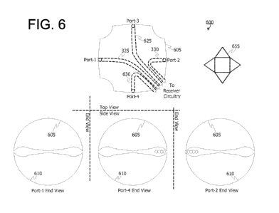
6 is a
mechanical drawing of a QPA. It shows a pair of PxMA elements that share a
common pair
of conductive surfaces 605 and 610, where one pair of ports, or port-pair, is
oriented
orthogonally to the other port-pair. One DPA uses a port-pair comprised of
port-1 and port-2
in FIG 6. The other DPA uses a port-pair comprised of port-3 and port-4 in FIG
6. FIG 7 is a
mechanical drawing of another QPA embodiment where a pair of DPAs share a
common pair
of conductive surfaces 705 and 710, where one port-pair is oriented
orthogonally to the other
port-pair. One DPA uses the port-pair comprised of port-1 and port-2 in FIG 7.
The other
DPA uses the port-pair comprised of port-3 and port-4 in FIG 7. The QPA has
the same shape
flexibility as the DPA, allowing the antenna to be optimized for various load
impedances and
to fit in the space needed by different applications.7
[0045] The invention also discloses a hex or six (6) port PxMA antenna
(HPA) and a
twelve (12) port or dual hex-port PxMA antenna (DHPA) that operate to
arbitrarily low
frequency, and its use in a DF system. These are useful for a minimum size 3D
and fully
polarimetric RF emitter sensing device embodiments. Rather than using three
DPAs or three
QPAs that are oriented orthogonally to each other, an embodiment can use a
single HPA or
DHPA, which allows three DPAs or QPAs to share the same volume. In other
words, all six
HPA ports or all twelve DHPA ports share the same space. The spatially merged
antenna
allows tighter manufacturing tolerances on keeping the twelve ports
orthogonal, tighter
mutual calibration, and a smaller total volume to support six orthogonal
ports, or twelve
ports. FIG 19B, is a mechanical drawing showing the DHPA configuration, while
FIG 19A
shows an HPA configuration. FIG 19B shows three pairs of conductive surfaces,
a first pair
1 a and lb having two pairs of ports, a second pair of conductive surfaces 2a
and 2b having
two pairs of ports, and a third pair of conductive surfaces 3a and 3b having
two pairs of ports.
The HPA in FIG 19A is a subset with one set of ports removed such that only
one pair of
ports for each pair of conductive surfaces remain. The conductive surfaces in
FIG 19A and
19B are shown with a flat and square main body on the faces of a cube. But
these surfaces
can take on other shapes such as being circular instead of square, or being
non-flat (such as
forming the shape of a sphere instead of a cube). Similarly, part of the
conductive surfaces
appear as thin wires that connect the main body of the conductive surfaces to
the feed points,
--10--
CA 02954985 2017-01-12
WO 2016/053441
PCT/US2015/040328
but the conductive surface can be shaped such that these connections have
other shapes, such
as being triangular tapers with the same shape flexibility as a DPA or QPA. In
addition to
obtaining a smaller total volume, the spatially merged antenna (1) operates
better in a
multipath environment since all six EM fields are measured in the exact same
location, (2)
allows tighter manufacturing tolerances for keeping the ports fixed relative
to each other (e.g.
orthogonal), and (3) achieves tighter mutual calibration. In any embodiment
where surfaces
have more than one port-pair (e.g. QPA, HPA, DHPA), the surface may be split
into a pair of
slightly offset surfaces so that each port-pair connects to a separate
surface. In all cases
(DPA, QPA, HPA, DHPA) there is also flexibility to place slits or slit
patterns in the
conductive surfaces to force currents to flow in preferred directions and at
preferred
frequencies if desired. Frequency selective surfaces may be used to operate at
preferred
frequencies, and be relatively invisible or reflective at other frequencies.
[0046] Multi-port antennas can be conceptually cut in half, where port-
pairs are split
between the two halves, such that the first-half of the multiport antenna is
the half of the
antenna that the signal arrives at first, and the other-half is the half that
the signal arrives at
after it passes the first half. In this case, the ports in the first half
output a signal that is
proportional to the sum of the magnitude of the E and H fields since the E and
H fields have
the same sign. The ports in the other half output a signal that is
proportional to the difference
between the magnitude of the E and H fields since the E and H fields have
opposite signs. If
the antenna's sensitivity to the E and H fields are matched, both the sum and
the difference
output voltages have cardiod patterns but the cardiod patterns point in
opposite directions.
This sum and difference operation is shown pictorially in FIG 11.
[0047] As shown in FIG. 1A, the invention discloses an RF-emitter sensing
device
including an antenna circuit and an estimator configured to output, for one or
more incoming
signals-of-interest (Sol), one or more of (a) an estimated range to the
emitter of each Sol, (b)
estimates for one or more angles corresponding to the 3D angle-of-arrival
(AoA) of each Sol,
and (c) an estimated polarization of each Sol.
[0048] In this case, the antenna circuit has a plurality of ports that each
output an output
signal containing the one or more Sol. The antenna circuit includes one or
more multi-port
antennas. Each multi-port antenna has two or more ports. Each multi-port
antenna is
configured to pick up a combination of one or more vectors of the E-field
signal and one or
more vectors of the H-field signal from each Sol, from a common volume of
space, or in
other words, the same or identical volume of space. The estimator element is
configured to
--11--
CA 02954985 2017-01-12
WO 2016/053441
PCT/US2015/040328
output, for each Sol, one or more of (a) an estimated range, (b) an estimated
AoA, and (c) an
estimated polarization. It estimates one or more angles corresponding to the
AoA of each Sol
by receiving the output signals from the antenna circuit, and generating one
or more of an
estimated range to the emitter of each Sol, and estimates for one or more
angles
corresponding to the AoA of each Sol and an estimated polarization. The multi-
port antenna
is configured such that the one or more E-field signals and the one or more H-
field signals
can be isolated from each other by combining the output signals from the
various ports. Each
multi-port antenna can also be configured such that each port has a nominally
cardioid beam
pattern in all planes containing a common axis of symmetry about the cardioid
beam pattern.
Nearly ideal cardioid beam patterns are generated by adding and subtracting
weighted
versions of the isolated E-field and H-field signals.
[0049] If needed in particular applications, the estimator may also be
configured to isolate
particular signals of interest from other extraneous signals and noise. Figure
1B is a block
diagram similar to FIG lA but that explicitly shows an isolator element.
[0050] In some applications, the isolator function can be configured at the
time of
manufacturing to address well known signals in the intended application. In
other
applications it is advantageous to allow a user to specify parameters that
identify one set of
characteristics that represent the desired signal and another set of
characteristics that
represent interference that should be rejected. Similarly, in some
applications, the estimator
can be configured to output specific items such as AoA or range or
polarization outputs. In
other applications it is advantageous to allow a user to define the items they
want the system
to output. To address this variety of needs, FIG 1A and FIG 1B show a user
input path that
sometimes may not be used, but other times may be used for defining parameters
for a set of
one or more Sol, or may be used to define a set of outputs needed, or may be
used to define
system states or configurations such as power-on, power-off, sleep, idle, etc.
or orientations
and locations of different ports in the antenna circuit, or the orientation of
the system relative
to something else, such as the orientation relative to the earth, or the
orientation relative to the
vehicle carrying the DF system.
[0051] As shown in FIG. 1B, a DF system is disclosed for determining the
AoA,
polarization, and range to the emitter of a signal that:
(1) contains or receives user data that includes items such as: (a) Sol-
isolation-
metrics that can be used to isolate the Sol, such as one or more of: the
center
--12--
CA 02954985 2017-01-12
WO 2016/053441
PCT/US2015/040328
frequency, bandwidth, modulation characteristics, occurrence timing,
polarization,
field strength, stability of field strength, constraints on the range of
potential
angles of arrival, and known multipath geometries; (b) a list specifying one
or
more desired outputs; (c) the antenna-system's port configuration; and (d) the
time
and date and pose (position and orientation, e.g., x-, y-, z-position and
roll, pitch,
yaw orientation) of a reference position on the DF system relative to an earth
coordinate system; and
(2) is comprised of:
(a) an antenna-system 101, with an output for each antenna element port, and
which includes one or more PxMA elements where the PxMA element is a pair of
conductive surfaces offset from one another comprised of a first conductive
surface and a second conductive surface with one or more pairs of ports, or
port-
pairs, wherein each port-pair has a first port and a second port, and wherein
each
port is formed by a connection to the two conductive surfaces, and wherein
each
port-pair forms a loop going from the first terminal of the first port,
through the
first conductive surface to the first terminal of the second port, through the
second
port to the second terminal of the second port, and through the second
conductive
surface to the second terminal of the first port, and through the first port
back to
the first terminal of the first port to complete the loop, and wherein when
there is
both a first port-pair and a second port-pair, the port-pairs are orthogonal
to one
another such that a construction line going between the first port-pair and a
construction line going through the second port pair are at 90 degrees to each
other, and;
(b) an isolation element 102 that (i) receives the antenna-system outputs,
(ii)
isolates the SoI on each port based on the SoI-isolation-metrics in the user
data,
and (iii) has an output with the isolated SoI corresponding to each antenna-
system
output; and
(c) an estimator element 103 that (i) receives the isolated SoI for each of
the
antenna-system ports from the isolation element, and (ii) estimates and
outputs the
list of desired outputs specified in the user data.
[0052] The list specifying desired outputs generally includes for each
particular SoI, one
or more items such as: the coordinate system, the RF emitter sensing system's
pose (position
--13--
CA 02954985 2017-01-12
WO 2016/053441
PCT/US2015/040328
& orientation) at the time of measurement of the SoI level, time and date,
which angles to
output (e.g. azimuth, elevation, or both), desired azimuth angle accuracy and
confidence
level, achieved azimuth angle accuracy and confidence level, desired elevation
angle
accuracy and confidence level, achieved elevation angle accuracy and
confidence level,
maximum processing time allowed, processing time used, time periods used to
integrate the
SoI energy, SoI polarization, center frequency, modulation type, peak-to-
average ratio,
variance, times to a number of the highest peaks, frequency-versus-time
profile, power-
versus-time profile, rms power, etc.
[0053] The antenna-system's port configuration includes items associated
with each port,
such as the position and beam pattern (including one or more of magnitude,
polarization,
group-delay, impulse-response, and transfer-function as a function of angles)
relative to a
reference position/orientation on the RF emitter sensing system.
[0054] The estimator element is configured to determine and output an angle-
of-arrival
(AoA) estimate of a signal-of-interest (SoI) in a manner that is unbiased to
homogeneous
noise in the environment, and to its own system noise including the low noise
amplifiers
(LNA) in its front end.
[0055] The estimator element is also configured to mitigate finite
tolerances in antenna
element dimensions and termination network impedances and losses. The
disclosed
mitigation method enhances the RF emitter sensing device's accuracy by making
it immune
to manufacturing tolerances.
[0056] The antenna system, in some embodiments, is configured to use
shadowing on all
or some of the sensor elements. Any antenna element that is made small enough,
can fit
within a small/short shadow behind a small reflective or absorptive barrier.
Operation in this
shadow region allows reduced sensitivity to particular wave fronts, such as a
skywave, while
retaining sensitivity to other wavefronts, such as a ground-wave. This
modified sensitivity
enhances the performance of the RF emitter sensing system in some
applications, such as
finding the AoA of near vertical incidence skywave (NVIS) signals. DPA, QPA,
HPA, and
DHPA elements are particularly suitable to operate in a shadowed mode since
they remain
directional even at extremely small size.
[0057] In other words, the invention discloses the an RF emitter sensing
device including
an antenna circuit and an estimator configured to output, for one or more
incoming signal-of-
interest (SoI), either or both of an estimated range to the emitter of each
SoI, and estimates
--14--
CA 02954985 2017-01-12
WO 2016/053441
PCT/US2015/040328
for one or more angles corresponding to the 3D angle-of-arrival (AoA) of each
SoI, wherein
the antenna circuit has a plurality of ports that each output an output signal
containing the one
or more SoI, the antenna circuit including one or more multi-port antennas,
each multi-port
antenna having two or more ports, each multi-port antenna being configured to
pick up a
combination of one or more E-field signals and one or more H-field signals
from each SoI, in
a common volume of space; and the estimator element is configured to output
either or both
of an estimated range to the emitter of each SoI, and estimates for one or
more angles
corresponding to the AoA of each SoI by receiving the output signals from the
antenna
circuit, and generating either or both of an estimated range to the emitter of
each SoI, and
estimates for one or more angles corresponding to the AoA of each SoI.
[0058] The invention also discloses the above RF emitter sensing device
wherein each
multi-port antenna is also (a) configured such that each port has a nominally
cardioid beam
pattern in all planes containing a common axis of symmetry about the cardioid
beam pattern,
or (b) configured such that the one or more E-field signals and the one or
more H-field
signals can be isolated from each other by combining the output signals, or
(c) configured to
pick up a combination of one or more E-field signals and one or more H-field
signals from an
SoI, such that, an output port on a first-half of a multiport antenna picks up
a sum of an E-
field signal and H field signal, creating a sum signal, while an output port
on an other-half of
the multiport antenna picks up a difference between an E-field signal and an H-
field signal,
creating a difference signal, wherein, the first-half of the multiport antenna
is the half of the
antenna that the SoI arrives at first, according to the Poynting vector, and
the other-half of the
multiport antenna is the half that is not the first half.
[0059] The invention also discloses the above RF emitter sensing device
wherein the
estimator circuit is also configured to mitigate extraneous signals and
isolate one or more
desired SoI from the antenna circuit's output signals.
[0060] The invention also discloses the above RF emitter sensing device
also receiving or
having access to user data that includes SoI isolation parameters or
characteristics
corresponding to one or more user-desired SoI wherein, the estimator element
is configured
to isolate the one or more user-desired SoI from other extraneous signals
according to the
SoI-isolation-parameters. Examples of SoI-isolation-parameters for an SoI
include time
intervals, time intervals when the SoI is known or likely to be active, time
intervals when the
SoI is known or likely to be inactive, time-frequency profile intervals, field
strength range,
center frequency, bandwidth, modulation characteristics, occurrence timing,
repetition rate,
--15--
CA 02954985 2017-01-12
WO 2016/053441
PCT/US2015/040328
polarization, stability of field strength, constraints on a range of potential
angles of arrival,
and multipath geometries.
[0061] The invention also discloses the above RF emitter sensing device
wherein
receiving or having access to user data including a list of desired outputs
associated with an
incoming signal, wherein: the list of desired outputs including either or both
of an estimated
range to the emitter of each SoI, and estimates for one or more angles
corresponding to the
Poynting vector of each SoI and may also include other metrics associated with
each SoI such
as: the antenna element locations used, the distance between the antenna
locations used, the
field strength, the pose of the RF emitter sensing device relative to some
other coordinate
system at the time the antenna outputs were measured, the time periods the
antenna outputs
were used, the desired accuracy, the desired confidence level, the achieved
accuracy, the
achieved confidence level, the maximum processing time allowed, the processing
time used,
the polarization of the SoI, the center frequency the SoI, the type of
modulation on the SoI,
the pulse repetition rate of the SoI if the SoI is pulsed, the peak-to-average
ratio of the SoI
over the period used, the variance in the SoI energy over the period used, a
number Pm,
representing the maximum peak level that occurred in the SoI during the time
period used, a
number Pr representing a level range factor, a number Npc that is the count of
signal peaks
that were within the range of Pm and Pm*Pr that occurred during the processing
of the SoI,
wherein Npc is governed by the user specifying Pr, or Pr is governed by the
user specifying
Npc, the time that each of the Npc peaks occurred, the frequency versus time
profile of the
SoI over the period used, the power versus time profile of the SoI over the
period used,
wherein the power units are specified, such as being an rms, average, quasi-
peak, peak, etc.,
one or more trigger signals, each indicating that a specific event occurred,
and the time of
occurrence of a specific event, wherein specific events are specified, such as
the occurrence
of or end of a time-frequency-power profile, and the estimator element is
configured to
generate and output the list of desired outputs
[0062] The invention also discloses the above RF emitter sensing device
also receiving or
having access to user data t that includes orientation information including
one or more of: a
definition for a local coordinate system on the RF emitter sensing device that
includes a
system reference position on the RF emitter sensing device; an antenna circuit
configuration
definition that includes locations, orientations, and beam patterns associated
with each of the
plurality of antenna ports relative to the local coordinate system on the RF
emitter sensing
device; and may also include other information such as time, date, and the
pose of the local
--16--
CA 02954985 2017-01-12
WO 2016/053441
PCT/US2015/040328
coordinate system on the RF emitter sensing device relative to another
coordinate system,
such as an earth coordinate system, or a ground or an air vehicle coordinate
system; and
wherein a beam pattern definition includes the response as a function of angle
for one or
more of: polarization-versus-frequency; group-delay; transfer function
magnitude versus
frequency; transfer function phase versus frequency; and impulse response.
[0063] The invention also discloses the above RF emitter sensing device
wherein the one
or more multi-port antennas include a multiport antenna that is comprised of
one or more
conductive-surface-pairs, wherein, each conductive-surface-pair has a first
conductive
surface, a second conductive surface offset in an offset-direction from the
first conductive
surface, and one or more port-pairs, each port-pair including a first port and
a second port;
wherein each of the first and second port is formed by a connection to the
first and second
conductive surfaces, and wherein each of the one or more port-pairs forms a
loop going from
a first terminal of a corresponding first port, through the first conductive
surface to a first
terminal of a corresponding second port, through a termination load connected
across the
corresponding second port to a second terminal of the corresponding second
port, and
through the second conductive surface to a second terminal of the
corresponding first port,
and through a termination load connected across the corresponding first port,
back to the first
terminal of the corresponding first port to complete the loop, and an output
for each port; and
wherein the different conductive-surface-pairs have different offset-
directions; and wherein
the loops associated with the port-pairs share a nominally common center
point. The
invention discloses the above RF emitter sensing device wherein all specific
embodiments of
the preceding multiport antenna are permissible, including a multiport antenna
with one
conductive surface pair wherein the surface pair attaches to one port-pair, or
two port-pairs,
or two port-pairs wherein there is an aiming axis associated with each port-
pair, lying in the
plane of the loop formed by each port-pair, that extends between each port-
pair such that it
intersects the center point between the terminals of the first port, and the
center point between
the terminals of the second port, wherein there is a polarization axis
orthogonal to the aiming
axis and lying in the plane of the loop formed by each port-pair, wherein the
two port-pairs
are oriented such that: their aiming axes are nominally orthogonal to each
other, their
polarization axes are nominally aligned to each other, and their loops
nominally share the
same center point.
[0064] Similarly, the invention discloses the above RF emitter sensing
device wherein the
above multiport antenna has three conductive surface-pairs wherein each
surface-pair
--17--
CA 02954985 2017-01-12
WO 2016/053441
PCT/US2015/040328
attaches to one port-pair, wherein each conductive-surface-pair has an offset
direction and
port-pair placement such that the aiming axes of the three port-pairs are
nominally orthogonal
to each other and the polarization axes of the three port-pairs are nominally
orthogonal to
each other, and the loops formed by the three port-pairs nominally share the
same center
point.
[0065] Similarly, the invention discloses the above RF emitter sensing
device wherein the
above multiport antenna has three conductive surface-pairs wherein each
surface-pair
attaches to two port-pairs, wherein each conductive-surface-pair has an offset
direction and
port-pair placement such that the aiming axes of the the two port-pairs on
each surface pair
are nominally orthogonal to each other and the polarization axes are aligned,
while the
polarization axes of the ports on any conductive surface pair is orthogonal to
the polarization
axis of the ports on the other conductive surface pairs, and the loops formed
by all the port-
pairs nominally share the same center point.
[0066] The invention also discloses the above RF emitter sensing device
wherein the
estimator element is configured to output either or both of an estimated range
to the emitter of
the incoming signal, and estimates for one or more angles corresponding to the
AoA of the
incoming signal by also computing the estimated range and/or one or more angle
estimates
based on a computation that is a function of the received output signals from
the antenna
circuit.
[0067] The invention also discloses the above RF emitter sensing device
wherein the
estimator element is configured to output either or both of an estimated range
to the emitter of
an SoI, and estimates for one or more angles corresponding to the AoA of an
SoI by also
computing the estimated range and/or one or more angle estimates based on a
computation
that is a function of: the received output signals from the antenna circuit,
and a set of one or
more baseline values determined with one or more known SoI, with each of the
one or more
known SoI at one or more known positions including one or more of a range and
one or more
angles.
[0068] The invention also discloses the above RF emitter sensing device
wherein the
estimator element is configured to output either or both of an estimated range
to the emitter of
an SoI, and estimates for one or more angles corresponding to the AoA of an
SoI by also:
computing the estimated range and/or one or more angle estimates based on a
computation
that is a function of: the received output signals from the antenna circuit,
and a set of one or
--18--
CA 02954985 2017-01-12
WO 2016/053441
PCT/US2015/040328
more baseline values determined with one or more known SoI, with each of the
one or more
known SoI at one or more known positions including one or more of a range and
one or more
angles. The invention also discloses the preceding RF emitter sensing device
wherein the
baseline values are stored.
[0069] The invention also discloses the above RF emitter sensing device
wherein the
estimator element is configured to output either or both of an estimated range
to the emitter of
an SoI, and estimates for one or more angles corresponding to the AoA of an
SoI by also,
computing the estimated range and/or one or more angle estimates based on a
computation
that is a function that uses the received SoI from the antenna circuit output
signals, wherein
the function includes: computing a set of weighted sums, where each weighted
sum is a sum
of weighted versions of the SoI from two or more output signals received from
two or more
ports of the antenna circuit, and wherein the weights can be positive,
negative, or complex.
[0070] The invention also discloses the above RF emitter sensing device
wherein the
estimator element is configured to output either or both of an estimated range
to the emitter of
an SoI, and estimates for one or more angles corresponding to the AoA of an
SoI by also:
computing the estimated range and/or one or more angle estimates based on a
computation
that is a function that uses the received output signals from the antenna
circuit, wherein the
function is configured to mitigate estimation bias caused by one or more of:
receiver noise,
noise picked up by the antennas, noise picked up by antennas that is
uncorrelated between
different ports, sensitivity imbalance in the E and H fields picked up by a
port, the magnitude
of an SoI, modulation of the SoI, effects of non-ideal termination impedances
attached to the
antenna ports, and the effects of objects causing reflections into the antenna
circuit or
blockages to the antenna circuit.
[0071] The invention also discloses the above RF emitter sensing device
wherein the
estimator element is configured to output either or both of an estimated range
to the emitter of
an SoI, and estimates for one or more angles corresponding to the AoA of an
SoI by also,
computing the estimated range and/or one or more angle estimates based on a
computation
that is a function that uses the received SoI from the antenna circuit output
signals, wherein
the function is configured to mitigate estimation bias caused by one or more
of: receiver
noise, noise picked up by the antennas, noise picked up by antennas that is
uncorrelated
between different ports, sensitivity imbalance in the E and H fields picked up
by a port, the
magnitude of an SoI, modulation of the SoI, effects of non-ideal termination
impedances
attached to the antenna ports, and the effects of objects causing reflections
into the antenna
--19--
CA 02954985 2017-01-12
WO 2016/053441 PCT/US2015/040328
circuit or blockages to the antenna circuit, by estimating an angle of arrival
from an (i, j) pair
of port-pairs, where the function uses arguments including one or more ratios,
A1/131 ,
AJ MJ and Bi/B,, , and where the function may include trigonometric functions,
lookup
table based functions, and functions based on measurements of SoI at known
angles, where
the trigonometric functions include functions such as inverse sine, inverse
cosine, inverse
tangent and four quadrant arctangent functions, such as the Fortran atan2(y,
x) function,
wherein: the terms, A,,B,,Ai,Bi, are either: A, = P1 ¨ P2,, , B, = P1 + P2,, ,
A = PLJ P2d
B =P1 + P2, or A1 = ¨Pt, B1 = +P, A = ¨ 2, j B = + P' and where
1,1 1,1 2,1
i and j are indexes, each of which represents a particular port-pair, where
each takes on an
integer value from 1 to N, and N is the number of port-pairs in the antenna
circuit, and the
(i, j) pair of port-pairs is a set of ports comprised of the ith port-pair and
a ith port pair,
wherein, j is not equal to i, the ports in both port-pairs share the same
polarization, the
patterns of the first port and the second port in each of the port-pairs are
aimed in opposite
directions defining an aiming axis, the aiming axis of the ith port-pair is
orthogonal to that of
the ith port-pair, and wherein pi, is an initial SoI amplitude derived from
the first port of the
ith port-pair, and similarly is an initial SoI amplitude derived from the
first port of the jth
port-pair, and wherein P2',1 is an initial SoI amplitude derived from the
second port of the ith
port-pair, and similarly P2' j is an initial SoI amplitude derived from the
second port of the jth
port-pair, and wherein a set of weighted sums is comprised of, a first
quantity, PL, which is a
corrected amplitude for the SoI at the first port of the ith port-pair, and a
second quantity
which is a corrected amplitude for the SoI at the second port of the ith port-
pair, and wherein
the set of weighted sums is created as: PL, = (a, +1)111 + (a, ¨1)P; , and
= c1kb1+1)P2',1+(b1-1)13:ii where: the weights in the weighted sum are
(a, +1), (a, ¨1), (b, +1), and (b,-1) , and where a, and b, are chosen such
that, for the SoI, the
beam pattern of PL, is cardiod with a single deep null in a first direction,
the beam pattern of
P is cardiod with a single deep null in a second direction, wherein the first
direction and
second direction are nominally 180 degrees from each other, and c, .is chosen
such that the
peaks of the main lobes of PL, and P are equal.
--20--
CA 02954985 2017-01-12
WO 2016/053441
PCT/US2015/040328
[0072] The invention also discloses the above RF emitter sensing device
wherein the
estimator element is configured to output either or both of an estimated range
to the emitter of
an SoI, and estimates for one or more angles corresponding to the AoA of an
SoI by also,
computing the estimated range and/or one or more angle estimates based on a
computation
that is a function that uses the received SoI from the antenna circuit output
signals, wherein
the function is configured to mitigate estimation bias caused by one or more
of: receiver
noise, noise picked up by the antennas, noise picked up by antennas that is
uncorrelated
between different ports, sensitivity imbalance in the E and H fields picked up
by a port, the
magnitude of an SoI, modulation of the SoI, effects of non-ideal termination
impedances
attached to the antenna ports, and the effects of objects causing reflections
into the antenna
circuit or blockages to the antenna circuit, by estimating an angle of arrival
from an (i, j) pair
of port-pairs, where the function uses arguments including one or more of
A,/(B, ¨ ),
A/(3 ¨ ) and (B, ¨ ¨ and where the function may include trigonometric
J J
functions, lookup table based functions, and functions based on measurements
of SoI at
known angles, where the trigonometric functions include functions such as
inverse sine,
inverse cosine, inverse tangent and four quadrant arctangent functions, such
as the Fortran
atan2(y,x) function, wherein: the terms, A, B,, Ai, B, are either: A, = P11 ¨
P2,, ,
B =P +P A =P ¨P B =P +P or A = ¨P1 B =P1 +P1
1 1,1 2,1 , 2, j 2, j 1 1,1 2,1, 1 1,1 2,1 ,
A = ¨ B = + T2dy, and where i and j are indexes, each of which
represents a
id
particular port-pair, where each takes on an integer value from 1 to N, and N
is the number
of port-pairs in the antenna circuit, and the (i, j) pair of port-pars is a
set of ports comprised
of the ith port-pair and a jth port pair, wherein, j is not equal to i, the
ports in both port-
pairs share the same polarization, the patterns of the first port and the
second port in each of
the port-pairs are aimed in opposite directions defining an aiming axis, the
aiming axis of the
ith port-pair is orthogonal to that of the jth port-pair, and wherein /3: is
an initial SoI
amplitude derived from the first port of the th port-pair, and similarly
/31',. is an initial SoI
amplitude derived from the first port of the jth port-pair, and wherein P2'1
is an initial SoI
amplitude derived from the second port of the ith port-pair, and similarly P2'
j is an initial SoI
amplitude derived from the second port of the jth port-pair, and wherein a set
of weighted
sums is comprised of, a first quantity, PL, which is a corrected amplitude for
the SoI at the
--21--
CA 02954985 2017-01-12
WO 2016/053441
PCT/US2015/040328
first port of the th port-pair, and a second quantity P2õ , which is a
corrected amplitude for the
SoI at the second port of the ith port-pair, and wherein the set of weighted
sums is created as:
Piõ = (a, +1)13: +(a, ¨1)13, and P2õ = cikb,+1)13+ (b, ¨1)F1'i where: the
weights in the
weighted sum are (a, +1), (a, ¨1), (b, +1), and (b1 ¨1) , and where a, and b,
are chosen
such that, for the SoI, the beam pattern of põ is cardiod with its single deep
null in a first
direction, and the beam pattern of P2 is cardiod with its single deep null in
a second
direction, and the first direction and second direction are nominally 180
degrees from each
other, and c, .is chosen such that the peaks of the main lobes of põ and P2,
are equal, and the
factor to mitigate homogeneous noise, can be computed by functions
including:
= =4:13(A,,B,,AJ,BJ)= Re ¨ + ¨ ¨
¨ + H ¨ + I H I 3E
2 2 V6 4 144 3 4 144 V/ + 36H + 24F
wherein E=Ai2B1¨A;13,¨A,2Bi+A;13j, F=A,2 +B,2/2 ¨ BiBi +A;' +13 j2 12,
G = (B B )2(4A,2 ¨B2 +2BB +4A2 ¨B),
J
H1 V3(432E4 ¨ 64E2F3 +G(16F4 ¨144E2F)+ 8F2G2 + G3)172+ , and
=
A E2I2¨ F3127 +G(2BiBi¨ 2'41,2 ¨B ¨2A j2 _B)/24
if H #0
0 if H=O
[0073] The invention also discloses the above RF emitter sensing device
wherein the
estimator element is configured to output either or both of an estimated range
to the emitter of
an SoI, and estimates for one or more angles corresponding to the AoA of an
SoI by also:
computing the estimated range and/or one or more angle estimates based on a
computation
that is a function that uses the received output signals from the antenna
circuit, wherein the
function is configured to mitigate estimation bias caused by receiver noise
and noise picked
up by the antennas, by coherently deriving the amplitude of the SoI on each
port, by
correlating the signal from each port in a port pair, over a time period which
may be
continuous or discontinuous, with a signal that is a combination of the
signals from one or
more ports that do not include the ports in the port-pair, where the
combination of signals
includes, selecting one or more porta and summing their signals, selecting one
or more ports
and weighting and summing their signals, selecting the port with the largest
signal from
--22--
CA 02954985 2017-01-12
WO 2016/053441
PCT/US2015/040328
among the available ports and using its signal, and using maximum ratio
combining (MRC)
to weight and sum the signals from two or more of the ports.
[0074] The invention also discloses the above RF emitter sensing device
wherein the
estimator means is configured to output either or both of an estimated range
to the emitter of
an SoI, and estimates for one or more angles corresponding to the AoA of an
SoI by also
using one or more of: one or more magnitudes from one or more combinations of
the output
signals from among the different ports of the antenna circuit, and one or more
phases from
one or more combinations of the output signals from among the different ports
of the antenna
circuit. The invention also discloses the preceding RF emitter sensing device
wherein the
above weights applied to the one or more combinations are stored. The
invention also
discloses the preceding RF emitter sensing device wherein the one or more
combinations of
output signals includes combinations that isolate the E-field of the SoI and
that isolate the H-
field of the SoI.
[0075] The invention also discloses the above RF emitter sensing device
wherein the
antenna circuit is configured to pick up signals at a more than one location
or orientation, and
the one or more locations or orientations are made with one or more of a
sequential
configuration and a simultaneous configuration; wherein, in the sequential
configuration,
ports are in respective initial locations and orientations at an initial time,
and ports are in a
respective next location and orientation at a next time that is later than the
initial time, and
wherein the estimator uses the output signals received at different times.
[0076] The invention also discloses an RF emitter sensing device comprising
an antenna
circuit, an isolation element, and an estimator element configured to output,
for one or more
incoming signal-of-interest (SoI), either or both of an estimated range to the
emitter of each
SoI, and estimates for one or more angles corresponding to the angle-of-
arrival (AoA) of
each SoI, wherein: the antenna circuit has a plurality of ports that each
output an output
signal containing the one or more SoI, the antenna circuit including one or
more multi-port
antennas, each multi-port antenna having two or more ports, each multi-port
antenna being
configured to pick up a combination of one or more E-field signals and one or
more H-field
signals from each SoI, in a common volume of space, such that the one or more
E-field
signals and the one or more H-field signals can be isolated from each other by
combining the
output signals; and the isolation element is configured to output one or more
isolated SoI
outputs, for each respective port by receiving the output signals from each
output port of the
antenna circuit, and isolating in each respective port, one or more SoI from
other extraneous
--23--
CA 02954985 2017-01-12
WO 2016/053441
PCT/US2015/040328
signals; and the estimator element is configured to output either or both of
an estimated range
to the emitter of each SoI, and estimates for one or more angles corresponding
to the AoA of
each SoI by: receiving the output signals from the isolation element, and
generating either or
both of an estimated range to the emitter of each SoI, and estimates for one
or more angles
corresponding to the AoA of each SoI.
[0077] The invention also discloses the preceding RF emitter sensing device
wherein the
estimator element is configured to output either or both of an estimated range
to the emitter of
an SoI, and estimates for one or more angles corresponding to the AoA of an
SoI by also:
computing, for each SoI, a set of measured values based on the one or more
isolated SoI
outputs from the isolation element, comparing, for each SoI, the set of
measured values with
a plurality of sets of calibration values, where the plurality of sets of
calibration values is
comprised of sets of values determined with the SoI emitter at a known, one or
more of,
location, AoA, and range.
[0078] The invention also discloses the preceding RF emitter sensing device
wherein the
one or more multi-port antennas include a multiport antenna that is comprised
of one or more
conductive-surface-pairs, wherein, each conductive-surface-pair has a first
conductive
surface, a second conductive surface offset in an offset-direction from the
first conductive
surface, and one or more port-pairs, each port-pair including a first port and
a second port;
wherein each of the first and second port is formed by a connection to the
first and second
conductive surfaces, and wherein each of the one or more port-pairs forms a
loop going from
a first terminal of a corresponding first port, through the first conductive
surface to a first
terminal of a corresponding second port, through a termination load connected
across the
corresponding second port to a second terminal of the corresponding second
port, and
through the second conductive surface to a second terminal of the
corresponding first port,
and through a termination load connected across the corresponding first port,
back to the first
terminal of the corresponding first port to complete the loop, and an output
for each port; and
different conductive-surface-pairs have different offset-directions and the
loops associated
with the port-pairs share a nominally common center point.
[0079] The invention also discloses the above RF emitter sensing devices
wherein the
antenna circuit is configured such that the ports, including those from one or
more multiport
antennas, can be combined to provide three orthogonal E-field terms and three
orthogonal H-
field terms (e.g. Ex, Ey, Ez and Hx, Hy, Hz), and the estimator is configured
to estimate the
--24--
CA 02954985 2017-01-12
WO 2016/053441
PCT/US2015/040328
three dimensional Poynting vector of each SoI from the antenna circuit's
outputs and output
the three dimensional AoA for each SoI.
[0080] The invention also discloses the preceding RF emitter sensing device
also
receiving or having access to user data that includes SoI-isolation-parameters
corresponding
to each SoI wherein, the isolation element is configured to isolate the one or
more SoI from
other extraneous signals according to the SoI-isolation-parameters. The
invention also
discloses the preceding RF emitter sensing device wherein the SoI-isolation-
parameters
include one or more of, time intervals when the SoI is known or likely to be
active, time
intervals when the SoI is known or likely to be inactive, field strength
range, center
frequency, bandwidth, modulation characteristics, occurrence timing,
repetition rate,
polarization, field strength range, stability of field strength, constraints
on a range of potential
angles of arrival, and multipath geometries.
[0081] The invention also discloses the preceding RF emitter sensing device
wherein the
estimator element is configured to output either or both of an estimated range
to the emitter of
an SoI, and estimates for one or more angles corresponding to the AoA of an
SoI by also
computing the estimated range and/or one or more angle estimates based on a
computation
that is a function of the received output signals from the antenna circuit,
and a set of one or
more baseline values determined with one or more known SoI, with each of the
one or more
known SoI at one or more known positions including one or more of a range and
one or more
angles. The invention also discloses the preceding RF emitter sensing device
wherein the
baseline values are stored.
[0082] BRIEF DESCRIPTION OF THE DRAWINGS
[0083] The accompanying figures, where like reference numerals refer to
identical or
functionally similar elements and which together with the detailed description
below are
incorporated in and form part of the specification, serve to further
illustrate an exemplary
embodiment and to explain various principles and advantages in accordance with
the present
invention.
[0084] FIG 1A is a block diagram of an RF emitter sensing system;
[0085] FIG 1B is a block diagram of an RF emitter sensing system similar to
FIG 1A but
with an explicit isolation element.
[0086] FIG 2A is a picture of a transmission line version of a DPA;
--25--
CA 02954985 2017-01-12
WO 2016/053441
PCT/US2015/040328
[0087] FIG 2B is a picture showing an array of two transmission line
version DPA
antennas oriented at 90 degrees to each other according to a disclosed
embodiment, where
each antenna element is similar to the one shown in FIG. 3;
[0088] FIG 3 is a mechanical drawing of a transmission line version DPA
where the two
ports share a common spatial aperture that produces opposite facing cardioid
patterns from
the two ports for use in the RF emitter sensing system according to a
disclosed embodiment;
[0089] FIG. 4 is a mechanical drawing of a transmission line version DPA in
an
unbalanced configuration;
[0090] FIG 5 is a mechanical drawing for a 100 ohm balanced cylindrical
DPA;
[0091] FIG. 6 is a mechanical drawing showing a nominally spherical quad-
port antenna
(QPA) that is a pair of DPAs that are oriented orthogonally to each other and
that share the
same conductive surfaces;
[0092] FIG. 7 is a mechanical drawing for a alternative embodiment of a QPA
constructed
almost identically as the spherical QPA, but is cubical instead of spherical;
[0093] FIG. 8 shows a balanced DPA with its top covered by an absorbing
and/or
reflective layer which shields or shadows the antenna;
[0094] FIG. 9 shows a balanced DPA with both its top and its bottom covered
by
absorbing and/or reflective layers which shield or shadow the antenna from
waves coming
down toward the top of the antenna, or coming up toward the bottom of the
antenna useful for
elevated applications such as on aircraft;
[0095] FIG. 10 shows an unbalanced DPA with its top covered by an absorbing
and or
reflective layer, which shield or shadow the antenna from waves coming down
toward the top
of the antenna;
[0096] FIG. 11 is a drawing illustrating the theory of operation of a DPA,
including
showing a side view of a DPA along with solid or dashed arrows to illustrate a
wave coming
directly into either the right (dashed) or left (solid) ports of the antenna,
along with the
direction of the current induced by the magnetic field, and the voltage
induced by the electric
field, according to a disclosed embodiment.;
[0097] FIG. 12 shows an antenna-system with sixteen ports;
--26--
CA 02954985 2017-01-12
WO 2016/053441
PCT/US2015/040328
[0098] FIG. 13 shows an embodiment with an antenna-system comprised of 18
ports, an
isolation element with 18 parallel channels, including a switch network and
calibration signal
generator that allow full system calibration as well as built-in test
capability to confirm all
wiring;
[0099] FIG. 14 shows a low-cost embodiment in which the antenna-system has
14 ports,
the isolation element has only two coherent receivers and includes a switch
network that
allows any antenna to connect to either receiver and allows system
calibration;
[00100] FIG. 15 illustrates the spherical coordinate system used to express
the DPA's
output voltage versus the angle and polarization of the incoming wave;
[00101] FIG. 16 illustrates magnitude patterns when e(2) is positive,
negative, or ideal,
where e(2) represents an imbalance between the electric dipole moment and the
magnetic
dipole moment, or an error caused by a phase shift due to operating the DPA at
a high
frequency;
[00102] FIG. 17 shows a theoretical pattern along with overlaid measured
points showing
the very close match between the theoretical 2-parameter model and the
measured beam
pattern shape in the critical 45 to 135 degree sector according to a disclosed
embodiment;
[00103] FIG. 18 is a plot showing the error between a simple 2-parameter
theoretical beam
pattern and the measured beam pattern according to a disclosed embodiment;
[00104] FIG. 19A is a mechanical drawing showing a 6-port-13 cross rn antenna
(6-PA)
also called a hex port antenna (HPA) that is cubical, which can replace three
DPAs that are
oriented orthogonally to each other;
[00105] FIG. 19B is a mechanical drawing showing a 12-port-13 cross in antenna
(12-PA)
also called a dual hex port antenna (DHPA) that is cubical, which can replace
three QPAs
that are oriented orthogonally to each other; and
[00106] FIG. 20 is a three-dimensional drawing with rectangular-box
representations of
three DPAs similar to those in FIG 3, oriented to enable their six ports to
collect all six EM
components. Following from FIG 11, electromagnetic components Ely, Ey, Ez
shown in FIG
20 create a voltage across the two conductive surfaces in the three respective
DPAs. Currents
, , I, induced in the loop formed by the ports and the conductive surfaces
in the
--27--
CA 02954985 2017-01-12
WO 2016/053441
PCT/US2015/040328
respective DPAs result from the respective H-field components 11,,Hy,Hz, shown
in FIG
20.
DETAILED DESCRIPTION
[00107] The instant disclosure is provided to further explain in an enabling
fashion the best
modes of performing one or more embodiments of the present invention. The
disclosure is
further offered to enhance an understanding and appreciation for the inventive
principles and
advantages thereof, rather than to limit in any manner the invention. The
invention is defined
solely by the appended claims including any amendments made during the
pendency of this
application and all equivalents of those claims as issued.
[00108] It is further understood that the use of relational terms such as
first and second, and
the like, if any, are used solely to distinguish one from another entity,
item, or action without
necessarily requiring or implying any actual such relationship or order
between such entities,
items or actions. It is noted that some embodiments may include a plurality of
processes or
steps, which can be performed in any order, unless expressly and necessarily
limited to a
particular order; i.e., processes or steps that are not so limited may be
performed in any order.
[00109] Much of the inventive functionality and many of the inventive
principles when
implemented, may be supported with integrated circuits (ICs), RF amplifiers,
RF switches,
mixers, analog-to-digital converters, digital-to-analog converters, direct
digital synthesis
(DDS) ICs, phase locked loop (PLL) and voltage controlled oscillator (VCO)
ICs,
microcontrollers, microprocessors, field programmable logic array (FPGA) ICs,
digital signal
processing (DSP) ICs, dynamic random access memory (DRAM) devices, static
random
access memory (SRAM) devices, or the like. In particular, they may be
implemented using
semiconductor processes and transistors such as FET, (including HFET, HEMT, E-
PHEMT,
PHEMT, MESFET, JFET, MOSFET, CMOS, etc.), BJT ( including HBT, etc), and
BiCMOS. It is expected that one of ordinary skill, notwithstanding possibly
significant effort
and many design choices motivated by, for example, available time, current
technology, and
economic considerations, when guided by the concepts and principles disclosed
herein will
be readily capable of generating the required circuitry with minimal
experimentation.
Therefore, in the interest of brevity and minimization of any risk of
obscuring the principles
and concepts according to the present invention, further discussion of such
ICs will be limited
to the essentials with respect to the principles and concepts used by the
exemplary
embodiments.
--28--
CA 02954985 2017-01-12
WO 2016/053441
PCT/US2015/040328
OVERVIEW
[00110] Disclosed is an ultra miniature RF emitter sensing device that does
passive ranging
and provides EM wave properties such as the Angle-of-Arrival (AoA) and
polarization. It
uses (1) an antenna system that includes unique miniature space-saving multi-
port /5 cross
in antenna (PxMA) elements that maintain their i3 cross in high directivity at
arbitrarily
low frequencies, and (2) signal processing methods that operate on the antenna
system's
outputs such that they (a) enable self sensitivity calibration, (b) mitigate
self noise, (c)
mitigate homogeneous environmental noise, (d) mitigate multipath such as from
sky-wave
versus ground-wave paths and such as from nearby metal structures, and (e)
enable accurate
AoA , polarization, and range to emitter characterization of signals so weak
that they are
below the noise floor of, and cannot be received by, a standard receiver
intended to receive
and demodulate the signal of interest. The resulting RF emitter sensing device
can be
extremely small size suitable for portable applications. It also has lower
complexity than
previous systems attempting to offer a similar bandwidth and frequency band of
operation.
Disclosed are miniature space-saving 4-port, 6-port, and 12-port PxMA antennas
that
maintain their /5 cross in high directivity to arbitrarily low frequencies.
The 12-port and 6-
port antennas provide all six E and H field components. Most RF applications,
including
previous DF systems, use one or both of two constitutive antenna elements, the
magnetic loop
antenna element that is sensitive to the H-field, which is sometimes
implemented as a slot
antenna, and the electric dipole/monopole antenna element that is sensitive to
the E-field.
Previously combinations of these elements created " cross ñ in a passband'
antennas. The
problem with these combined element antennas is that the termination
impedances and
sensitivities of the two elements are different and the network connecting
them do not allow
them to operate with high directivity to arbitrarily low frequency¨thus their
bandpass
characteristic. There exists, however, a third constitutive element that has
precisely collocated
electric dipole and magnetic moments /5 and th respectively, and where the
sensitivity to the
E and H fields are inherently matched and where a simple resistive termination
allows them
to be highly directional (i.e. high front-to-back ratio) to arbitrarily low
frequency¨which
means their direction finding ability at low frequencies does not degrade no
matter how
small this PxMA element is. Furthermore, the cardioid radiation pattern is
rotationally
symmetric about the axis of maximum radiation to arbitrarily low frequency. In
other words,
an E-plane cut and H-plane cut, or any cut going through the axis of maximum
and minimum
radiation, are identical. This symmetry property facilitates measuring a
wave's polarization
--29--
CA 02954985 2017-01-12
WO 2016/053441
PCT/US2015/040328
along with its angle-of-arrival. Disclosed is the use of this element,
including disclosed
miniature space-saving multi-port versions, in an RF emitter sensing system
that includes
disclosed signal processing methods allowing it to operate with high accuracy
at low, for
example HF (1-30 MHz) frequencies, yet be smaller and lighter than previously
thought
possible, such as being hand carried.
DEFINITION OF ANTENNAS - PxMA, DPA
[00111] In 1971 Reference 9 (SSN-125), in equation 12.27 on page 150 described
the
properties that make an ideal /5 cross Fri antenna (PxMA), where /5 refers to
the electric
dipole moment and in refers to the magnetic dipole moment. It is a radiator
that (a) has
collocated magnetic and electric dipole moments rn and /5 respectively, and
(b) these
moments are related in the late time (i.e. in the limit, at time goes to
infinity) such that
= c, where c is the speed of light. Reference 10 (SSN-243) states, "An ideal
ji cross Fri
radiator has some unique features that are not found in other elemental
radiators. They are
summarized in part as follows: (a) Cardioid radiation pattern rotationally
symmetric with the
axis of maximum radiation. (b) Purely real power out flowing from any
spherical surface
enclosing the source region. (c) Twice the directivity of a purely electric or
magnetic dipole."
The "other elemental radiators" referred to in the above quote refer to the
previously
mentioned dipoles/monopoles for electric fields, and loops for magnetic
fields. A key feature
of the PxMA is that its "late time" cardioid behavior extends, in the limit,
to infinite time.
This fact means that in the frequency domain, its cardioid behavior is
extremely wide
bandwidth and extends, in the limit, to DC. By using it in a small RF emitter
sensing system,
an RF emitter sensing system can be constructed that is inherently broad band
and works to
arbitrarily low frequencies without any dependence on matching networks or
tuning.
Reference 9 through Reference 16 address the theory, properties, and example
constructions
of PxMA elements.
[00112] We will use the term "DPA" to refer to a dual-port /5 cross in antenna
element
that operates with high directivity to arbitrarily low frequency. In other
words, a "DPA" is a
PxMA with two ports, or a port-pair. Reference 11 (SSN-319) describes an
embodiment of
such a DPA where the cardioid patterns from the two ports are aimed opposite
one another.
In this case the antenna is made with two conductive surfaces oriented and
shaped so they can
be thought of as a transmission line. FIG 2A is a picture of an embodiment of
this DPA. FIG
2B pictures a mockup of a pair of these DPAs oriented in orthogonal directions
and sharing a
--30--
CA 02954985 2017-01-12
WO 2016/053441
PCT/US2015/040328
common vertical polarization, where one DPA's port-pair aims north and south,
and the other
DPA's port-pair aims east and west. FIG 3 is a mechanical drawing of the DPA
pictured in
FIG 2A.
[00113] FIGs. 2A, 2B, and 3 show the DPA in a balanced configuration. The
antenna
element can be described as a pair of conductive surfaces offset from one
another with a pair
of ports, where each port is formed by a connection to the two conductive
surfaces such that a
loop is formed going from the first terminal of the first port, through the
first conductive
surface to the first terminal of the second port, through the second port to
the second terminal
of the second port, and through the second conductive surface to the second
terminal of the
first port, and through the first port back to the first terminal of the first
port to complete the
loop. In FIG 3, the pair of conductive surfaces are 305 and 310. In FIG 4, the
pair of
conductive surfaces are 305 and 460. In FIG 5, the pair of conductive surfaces
are 505 and
510. The configuration of FIG 3 is described in Reference 11. The
configuration of FIG 5 is
described in Reference 15. The width of these configurations can be narrowed
by making the
port connections not on the edges of the conductive surfaces.
[00114] In FIG 3 the conductive surfaces might be thought of as a transmission
line with a
top-wire 305 running left and right, and a bottom-wire 310 running left and
right, where the
ratio of separation between the wires and the width of the wires determine the
transmission
line impedance. When the width of both lines are the same, the transmission
line is balanced.
The plane between and parallel to the antenna's conductive plates (in other
words, between
the positive and negative terminals of the ports) is its ground-symmetry plane
since the
conductor above the symmetry plane the conductor below the symmetry plane are
a minor
image of one another. Each end of the transmission line 340A and 340B is a
balanced port.
The dimensions given in FIG 3 produce a 100 ohm balanced port that can be
connected viaa
100 ohm twinlead to a receiver. To use a standard unbalanced 50 ohm coaxial
cable 325 and
330, the balanced port can be connected through a balun, (i.e. transformer or
a splitter) 315
and 320 as is shown in FIG 3. For example, in the 1-750 MHz range, a
MinCircuits SBTCJ-
1WX would be suitable to use for the baluns 315 and 320. The polarities on the
baluns 315
and 320 are shown such that a vertically polarized wave coming into the side
of the antenna
produces a balanced differential signal on the two output coaxial cables 325
and 330. A
vertically polarized wave arriving on the main beam axis at 340A couples to
cable 325, but
does not couple to cable 330, providing excellent back-to-front ratio. A wave
coming straight
--31--
CA 02954985 2017-01-12
WO 2016/053441
PCT/US2015/040328
down from the sky, polarized so that the E-field is aligned to the axis going
through both
antenna ports, couples to both output coaxial cables 325 and 330 as a common
mode signal.
[00115] In FIG 3, symbols 350 and 355 are used in schematics such as FIGs 12,
13, and 14,
to represent the two ports and the orientation of a particular antenna element
port. The intent
is for the symbols to convey the polarization and directionality of a
particular physical
element.
[00116] FIG 4 is a mechanical drawing of this DPA in its unbalanced
configuration. In this
case the two conductive surfaces 305 and 460 are not the same size. The
transmission line
top-wire 305 running left and right, and a bottom-wire 460 running left and
right, are not the
same size. Conductive surface 460, due to its larger size, can be called a
"ground-plane" and
therefore the transmission line would be called unbalanced. This configuration
is effectively
one half (i.e. the top half) of the FIG 3 configuration, where conductive
surface 460 is in the
position of the ground symmetry plane of the FIG 3 configuration. The width of
460 should
extend beyond 305 by about the height shown in FIG 3. As before, the ports of
the antenna
are at the left and right ends of the transmission line, i.e. the edges of
conductive surface 305.
The dimensions given in FIG 4 produce 50 ohm ports that can be connected to
standard 50
ohm coaxial cables 325 and 330. These cables are typically terminated into a
receiver that
provides a 50 ohm match.
[00117] Any mismatch reflection off of the receiver will travel back through
the antenna to
the other antenna port, and thereby reduce the inherently excellent back-to-
front ratio of the
DPA element. If the receiver's complex reflection coefficient (e.g. S11) is
known at any
frequency of interest, and the cable 325, 330 electrical lengths and
attenuation are known,
then calibrations can be applied to restore the inherently excellent back-to-
front ratio of the
DPA element.
[00118] FIG 11 illustrates the theory of operation of the DPA. It shows a side
view of a
DPA along with solid 1105 and dashed 1110 arrows to illustrate a wave coming
directly into
either the right and left ports respectively. It also shows the direction of
the current loop
induced by the magnetic field with a solid 1115 and dashed 1120 curved arrows
associated
with waves 1105 and 1110 respectively. It also shows the voltage 1125 induced
by the
electric field, which is the same for both waves 1105 and 1110. By design, the
magnetic and
electric fields cancel at one port, and at the other port (where the wave
arrives), add to twice
what the E-field or H-field would have produced on their own The antenna's
inductance is
--32--
CA 02954985 2017-01-12
WO 2016/053441
PCT/US2015/040328
adjusted with the loop area (i.e. with length and height). The antenna's
capacitance, that is,
between the conductive surfaces 305 and 310 is adjusted with surface area and
height. The
termination impedance is set by the inductance and capacitance and matched by
designing the
balun transformers and low noise amplifier (LNA) to have the desired input
impedance. The
induced current and voltage add to produce an output voltage that is twice
what the E-field or
H-field would have produced on their own. It shows axes to illustrate the
right-hand rule
applied to the cross-product to get the Poynting vector from the E cross H,
and the right hand
rule to get the clockwise or counter-clockwise induced current from the H
field direction;
[00119] The loop area defined by the height of the transmission line and the
length
enclosed by the pair of port establishes the magnetic dipole moment of the
PxMA. The
electric dipole moment of the PxMA is governed by the spacing between the two
conductors
(i.e. the height of the antenna element) and the capacitance across the ports,
which is a
function of the size and shape of the two conductors. When the length and
width and height
and termination impedances are adjusted appropriately, as described in
Reference 11, the end
result is a dual port PxMA element, or DPA that maintains its unique PxMA
properties to
arbitrarily low frequencies, and with no matching network¨just a resistive
termination. Both
ports have a cardioid pattern, and the cardioid pattern is rotationally
symmetric about the
main beam axis.
[00120] Reference 15 (SSN-441) describes a DPA that is similar to the one in
Reference
11, but the conductive surfaces are cylindrical and do not form a transmission
line. FIG 5 is a
mechanical drawing for a 100 ohm balanced cylindrical DPA. Like FIG 3, there
is a top
conductive surface 505, a bottom conductive surface 510, with ports 340A and
340B at the
edges of these conductive surfaces. Coaxial cables 325 and 330 take the
signals from these
ports to receivers that can isolate different signals from one another. The
cylinder radius sets
the loop area and effective height. The width of the conductive surfaces sets
the capacitance.
Like the DPA of FIG 3, the loop area, capacitance, and termination resistance
are set so that
in the late time (i.e. as time goes to infinity), rii = cf3 . The magnetic and
electric dipole
moments hi and 12 are related by the speed of light c such that tit = cp so
that each port
generates a cardioid pattern that extends to arbitrarily low frequency without
any frequency
dependent matching network but with a simple fixed non-reactive termination.
Like the DPA
of FIG 3, the plane between and parallel to the antenna's conductive surfaces
(in other words,
between the positive and negative terminals of the ports) is its ground-
symmetry plane since
the conductor above the symmetry plane the conductor below the symmetry plane
are a
--33--
CA 02954985 2017-01-12
WO 2016/053441
PCT/US2015/040328
minor image of one another. Its cardioid pattern is symmetric along the axis
of the main
beam. Just as the balanced DPA of FIG 3 has an unbalanced version, as shown in
FIG 4, the
balanced cylindrical DPA of FIG 5 also has an unbalanced version where the
lower conductor
510 is replaced by a larger surface that serves as a ground-plane, allowing
the antenna to be
half the height.
[00121] The DPA is electrically small and generally lightweight and
inexpensive due to its
simple construction. The antenna ports are directional by virtue of the fact
that the antenna is
a PxMA¨the antenna's loop area, sensitive to the H-field, and antenna's
electric dipole
moment (or effective height), sensitive to the E-field, are inherently matched
to produce the
same voltage across a resistive port termination impedance. The termination,
in the case of an
RF emitter sensing system, is the input impedance of the receiver connected to
the port.
Because of its inherently matched E and H sensitivity at each port, the sum of
the E-field
induced signal and the H-field induced signal creates a null in one direction
and creates a
maximum response in the opposite direction¨i.e. the cardioid pattern ascribed
to a PxMA.
Because they are a true PxMA they have high directivity regardless of how low
the frequency
is¨in other words, they are not a structure with a passband nature, but could
be
infinitesimally small and still be directional. Both ports share the exact
same co-located
magnetic and electric dipole moments at arbitrarily low frequency. The fields
coupled to each
port come from the exact same spatial volume. As a result, their port ratios
are inherently
matched ports and they have a highly repeatable and stable ratio of gains at
any angle. If, due
to manufacturing tolerances, a DPA is slightly larger or smaller, the ports
still share the exact
same spatial aperture and volume and therefore have inherently matched gain
and
symmetrical patterns, even though the null in the cardioid may not be ideal.
Because the
sensitivity to mechanical tolerances is low, multiple DPAs are extremely well
matched to
each other, making them ideal for use in phased-array structures. In other
words, all of the
signal processing methods applied to arrays, such as those described in
Reference 5 can be
applied to an array that includes DPA elements.
[00122] Derived from Reference 15, the output voltage of a DPA versus
frequency and the
incidence angle of an incoming E-field follows the following proportion:
Vow (f 2 ,0,p,port_1).---zil(l+cos8)(E, sin0+ E0 cos0)
(1)
V out(f ,0,p,port _2) .---zil(1¨ cos 8)(E8 sin 0 + E0 cos0)
2
--34--
CA 02954985 2017-01-12
WO 2016/053441
PCT/US2015/040328
In this equation, A is the loop area of the antenna in square meters, A is the
wavelength in
meters, incident E-field (E0,E9) has units of volts/m, and K is in volts. The
angles 0 and
0 are expressed in the spherical coordinate system such as that shown in FIG
15. For
example, referring to FIG 15, suppose the X-Y plane is parallel to the earth's
surface, with
the Y-axis aimed north. Suppose the DPA is oriented so that its ports are on
the Z-axis and its
ground symmetry plane is the Z-X plane. To be clear, the DPA is oriented so
that its first
port, at positive Z, aims up toward the sky; its second port, at negative Z,
aims down to the
center of the earth; and the main beam from these ports is sensitive to a wave
polarized with
its E-field oriented along the y-axis, or north-south. The angle 0 is the
angle to the source of
the incident field relative to the aiming axis running through the two ports.
At 0 = 0 the
incident field arrives in the main beam of the first port. Note how, in
Equation 1, regardless
of 0, the beam pattern is always a raised cosine function of 0. This perfect
symmetry about
0 is useful for DF. We can define a plane that intersects both antenna ports
and the source of
the incident field which we will call the 0 -plane. This 0 -plane can be
visualized at a
particular 0 by imagining 0 spinning 360 degrees to define the 0 -plane. The
orientation of
the incident E-field (i.e. its polarization) is given in relation to this 0 -
plane. When 0 = 0 the
0 -plane is the ground-symmetry plane. The incident TEM (transverse electric
magnetic)
wave has E-field components that are perpendicular to the direction of energy
flow (i.e. the
Poynting vector) with one component, E9, in the 0 -plane, and the other
component, E0,
perpendicular to the 0 -plane. Note that the symmetry about the Z-axis is such
that if the
polarization were always oriented for the maximum response, the output voltage
would be
independent of 0 and only depend on 0.
[00123] To illustrate the antenna's response, rotate the coordinate system and
suppose a
DPA is oriented so that the first port aims north with vertical polarization.
In this case,
referring to FIG 15, the Z-axis would point to the north, the Z-X plane would
represent the
surface of the earth as well as the antenna's ground-symmetry plane, and the y-
axis would
aim toward the sky while the x-axis would aim west. In this vertical
polarization case, an E-
plane pattern is in a vertical plane containing both ports (i.e. the Z-Y
plane), and the H-plane
pattern is a horizontal plane that contains both ports (i.e. the Z-X plane).
[00124] Using this geometry, consider an E-plane beam pattern. In this case,
0= 900 and
0 spins 360 degrees to create the E-plane pattern. Here, 0 represents the
elevation angle. At
--35--
CA 02954985 2017-01-12
WO 2016/053441
PCT/US2015/040328
0 = 900, the 0 -plane is the E-plane and with vertical polarization E0 = 0 and
the E-field is
simply E9. Note that Et, is vertical to the earth (and coming from the
horizon) when 0 = 0
but when 0 = 90 , it is coming down from the sky, is horizontal to the earth
(with no vertical
component), and is aligned north-south along the axis running between the two
DPA ports.
At 0 = 45 , Et, is still coming from the north, but is coming down from the
sky and tilted at
an angle of 45 . At 0 =180 the E-field is coming from the south at the
horizon. E0 = 0
since there is no E-field perpendicular to the 0 = 900 0 -plane. Since E0 = 0,
Equation 1
shows that the E-plane pattern is
(2)
2
[00125] Next consider an H-plane beam pattern. In this case 0 = 00, and 0
spins 360
degrees to create the H-plane pattern. In this case 0 represents the azimuth
(or bearing)
angle. All fields in this plot come from a vertically polarized wave coming
from the horizon.
Since the vertically polarized E-field is perpendicular to the 0 = 00 0 -
plane, the E-field is
simply E0. In other words, since there is no horizontal E-field, i.e. no field
in the 0 -plane,
Et, = 0. At 0 = 0 , the field is vertical to the earth and coming in from the
north directly into
the first port. At 0 = 90 , the E-field is coming from the west. In this case,
Equation 1 shows
that the H-plane pattern is
(3)
2 0
[00126] A subscript nomenclature will be used to specify that a voltage came
from a
particular port orientation. For example, a receiver capable of isolating a
signal of interest
(Sol) connected to port-P has an output voltage on it of -IVO where t denotes
time and P
denotes the port. With earth centric compass aligned ports, the nomenclature
includes port
P e { Nv , Sv , Ev , W. } respectively referring to north, south, east, west,
and vertically
polarized, P e { NH, SH, EH, WO respectively referring to north, south, east,
west, and
horizontally polarized, and P e { UN, DN, UE, DE} respectively referring to up-
north,
(sensitive waves polarized north-south coming from the sky), down-north
(sensitive waves
polarized north-south coming from the ground), up-east (sensitive to an east-
west polarized
wave coming from the sky), down-east (sensitive to an east-west polarized wave
coming
--36--
CA 02954985 2017-01-12
WO 2016/053441
PCT/US2015/040328
from the ground). For example, for a north-south oriented and vertically
polarized DPA, the
receiver connected to port-N (the north port) has an output voltage of viv,
(t), while a receiver
connected to the south port has an output voltage of vs, (t). For brevity,
when discussing a
specific or representative case, like using a set of antennas that have only
vertically polarized
ports, these will be shortened to just viv(t) and vs (t), since vertical
polarization is understood
in the context of their use. Similarly, when simply referring to a single
arbitrarily aimed DPA
pairs ( 1),(0, and vs (t)) or ( vE(t) and 1),(0) or ( v, (t) and VD (t))will
be used to represent
the oppositely aimed port-pairs, regardless of how they might actually be
aimed in a fielded
system. The earth-centric compass-oriented nomenclature is used for simplicity
and clarity.
Clearly any particular set of ports can be rotated to any orientation which
can be
mathematically specified by standard geometric translation/rotation equations.
Antenna System
[00127] In one simple embodiment, the antenna-system is comprised of a single
DPA
element with two ports. Following FIG 1A, the estimator element is configured
to perform a
function F that produces an AoA estimate from the outputs of the two DPA
ports. Following
FIG 1B, the isolation element filters out all signals except for each of the
one or more signals
of interest (Sol) from each of the two DPA ports, and then the estimator
element performs a
function F that produces an AoA estimate for each of the isolated Sol. The
isolation element
can be comprised of a tuned filter or receiver at each port that isolates the
Sol from other
signals.
[00128] This simple single-DPA embodiment is useful when the operator can
rotate the
antenna, or when it is known that the AoA can only come from a particular side
of the DPA.
When it is known that the AoA can only come from a particular side of the DPA,
the function
F can use a port-pair measurement at a single DPA orientation to determine the
AoA. When
the AoA can come from either side of the DPA, the DPA can be rotated so that
the function F
can use measurements from more than one DPA orientation to determine the AoA.
Ambiguities, such as cos(x) = cos(-x) are resolved by rotating the DPA.
[00129] In another simple embodiment, the antenna-system is comprised of a DPA
plus
one or more additional antennas such that it has at least three ports. The
isolation element is
comprised of a tuned filter or a receiver at each port where all the receivers
are coherent. The
addition of at least one more port allows the Sol levels from the DPA ports to
be estimated
--37--
CA 02954985 2017-01-12
WO 2016/053441
PCT/US2015/040328
using a coherent process. The coherent Sol level estimation is done by
correlating each DPA
port output Sol with the Sol from one or more of the additional ports or a
weighted sum from
other ports. The correlation process can be done over a period of time that is
either
continuous or not continuous as will be described in greater detail later in
this document.
[00130] In another simple embodiment, the antenna-system has four ports and is
comprised
a set of two DPAs oriented orthogonally to each other, such as north-south and
east-west, or a
QPA. This embodiment, with both DPAs oriented for vertical polarization, would
be
appropriate for applications needing to find the AoA (or line of bearing
relative to north) of a
vertical ground-wave and where the antenna array is fixed and cannot be
rotated. By having
these four ports, calculations can be done to make the RF emitter sensing
system immune to
not only its own noise, but also homogeneous noise in the atmosphere picked up
by the
antennas. With both DPA antennas oriented for vertical polarization and
looking for a
ground-wave signal, both DPAs are working on an H-plane pattern, as described
in Equation
3 in paragraph [00125]. For this vertical ground-wave case, or application, we
will represent
the azimuth angle, where 0 = 0 is east and 0 = 90 is north. With this
definition, the voltage
out versus angle patterns for the four ports are:
147,,, cc (1+ sin 0)/2
Ws, cc ¨ sin 0)/2
(4)
WE, cc (i COS 02
Ww, cc ¨ COS 02
Quad-Port PxMA Antenna (QPA)
[00131] Rather than using a pair of DPAs that are oriented orthogonally to
each other,
another four-port embodiment could use a QPA, which is a pair of orthogonal
DPAs sharing
the same conductive surfaces. FIG 6 is a mechanical drawing showing a QPA that
is
nominally spherical. Like the DPAs of FIG 3 and FIG 5, it has a top conductor
605 and a
bottom conductor 610, and has the original two ports, or port-pair, port-1 and
port-2, and
coaxial cables 325 and 330, but now also has an additional second set of
ports, or port-pair,
port-3 and port-4, and coaxial cables 625 and 630. In this case the first pair
of ports produce
cardioid patterns aimed 0 and 180 degrees, while the additional pair of ports
(port-3 and port-
4) produce cardioid patterns aimed 90 and 270 degrees. Each port-pair form,
with the
conductive surfaces, a loop, where the two loops are orthogonal to each other.
The new
second magnetic dipole moment ñ for the port-3 port-4 pair is orthogonal to
the first
--38--
CA 02954985 2017-01-12
WO 2016/053441
PCT/US2015/040328
magnetic dipole moment hi, from the port-1 port-2 pair. As with all PxMA
elements, the
height, and width, and length, and termination impedances are generally setup
so WI, = ci, and
ri/2 = cy3 to obtain their unique symmetric cardioid pattern at arbitrarily
low frequency
performance with a resistive termination and no additional calibration.
[00132] Symbol 655 is a schematic symbol intended to pictorially represent 4
orthogonal
ports with polarization and directionality consistent with the QPA or a pair
of similarly
oriented DPA antennas.
[00133] FIG 7 is a mechanical drawing for an alternative embodiment of a QPA
constructed almost identically as the spherical QPA, with a top conductive
surface 705, a
bottom conductive surface 710, and the same port connections as FIG 6, but is
cubical instead
of spherical.
[00134] FIGs 6 and 7 show balanced versions of a QPA. Unbalanced versions can
be built
by replacing the lower conductor 610 or 710 with a conductor that is wide,
much like that
shown in FIG 4. In this case, the lower conductor is typically either a
square, with a width
that is on the order of 3 times or more the height of the sphere (FIG 6) or
cube (FIG 7), or
round with a diameter that is on the order of 3 times or more the height of
the sphere or cube
versions.
HPA and DHPA ¨ Hex Port Antenna and Dual Hex Port Antenna
[00135] Another embodiment useful for ultra-miniature 3D and fully
polarimetric DF
applications is an antenna system that includes one or more HPA or DHPA
elements. FIG
19A is a mechanical drawing showing an HPA and FIG 19B is a mechanical drawing
showing a DHPA. Rather than using three separate DPAs that are oriented
orthogonally to
each other, an HPA is three orthogonal DPAs that share a common volume.
Similarly, rather
than using three separate QPAs that are oriented orthogonally to each other, a
DHPA is three
orthogonal QPAs that share a common volume. As shown in FIG. 19A and 19B, both
the
HPA and DHPA are made with three pairs of conductive surfaces. Pair-1 is
comprised of
surface la, and surface lb. Pair-2 is comprised of surface 2a and 2b. Pair-3
is comprised of
surface 3a and 3b. Here, the numbers 1, 2, and 3 refer to opposing face-pairs
(i.e. faces on
opposite sides of cube 4 in FIG 19A and 19B) and where the letters a and b
refer to a specific
face in the face-pair. These conductive surfaces are shown as squares plus
wires but could
take on other shapes such as a circular or even a complex shape like a jig-saw
like piece.
--39--
CA 02954985 2017-01-12
WO 2016/053441
PCT/US2015/040328
[00136] Each face-pair, or pair of conductive surfaces, connect to either two
ports, if the
conductive surface pair are connected as a DPA, or connect to four ports if
the conductive
surface pair are connected as a QPA. Face-pair 1 (i.e. la and lb in FIG 19A
and 19B) has
ports 11, 12when connected as a DPA, and also has ports 13, and 14 when
connected as a
QPA. Face-pair 2 (i.e. 2a and 2b) has ports 21, 22 when connected as a DPA,
and also has
ports 23, and 24 when connected as a QPA. Face-pair 3 (i.e. 3a and 3b) has
ports 31, 32 when
connected as a DPA and also has ports 33, and 34 when connected as a QPA. Each
port, or
feed point, has a two terminals (e.g., + and ¨) that connect to their
respective conductive
surface. For clarity, the connection at the feed is shown being made through a
pair of "wires"
having equal length. These "wires" are, however, simply part of the conductive
surfaces and
can be shaped, such as in a triangular sheet. Port 11 connects through the
pair of wires where
the first wire in the pair is lal (going to face la) and the second wire in
the pair is lbl (going
to face lb). Port 12 connects through the pair of wires 1a2 (going to face la)
and 1b2 (going
to face lb). Port 13 connects through the pair of wires 1a3 (going to face la)
and 1b3 (going
to face lb). Port 14 connects through the pair of wires 1a4 (going to face la)
and 1b4 (going
to face lb). Face la plus wires la 1, 1a2, 1a3, 1a4 form a conductive surface.
Face lb plus
wires lbl, 1b2, 1b3, and 1b4 form another conductive surface. These two
conductive
surfaces and four ports form a first QPA. Port-11 and port-12 form a port-
pair, and port-13
and port-14 form a port pair such that the port-pairs are orthogonal to each
other. Each port-
pair can be connected to twinlead or a balun transformer or 180-degree
splitter or hybrid. A
connection of this type is illustrated in FIG 3. Instead of wires, the
conductive surface can be
shaped and bent, or be comprised of bonded pieces to provide these
connections, such as
using triangular wedges similar to those of FIG 7 instead of wires.
[00137] A second QPA orthogonal to the first QPA is constructed similarly.
Port 21
connects through the pair of wires 2a1 (going to face 2a) and 2b1 (going to
face 2b). Port 22
connects through the pair of wires 2a2 (going to face 2a) and 2b2 (going to
face 2b). Port 23
connects through the pair of wires 2a3 (going to face 2a) and 2b3 (going to
face 2b). Port 24
connects through the pair of wires 2a4 (going to face 2a) and 2b4 (going to
face 2b). These
four ports are equivalent to a second QPA, that is orthogonal to the first
QPA, where port-21
and port-22 form a port-pair, and port-23 and port-24 form a port pair where
the port-pairs
are orthogonal to each other.
[00138] A third QPA orthogonal to both the first and second QPAs is
constructed similarly.
Port 31 connects through the pair of wires 3a1 (going to face 3a) and 3b1
(going to face 3b).
--40--
CA 02954985 2017-01-12
WO 2016/053441
PCT/US2015/040328
Port 32 connects through the pair of wires 3a2 (going to face 3a) and 3b2
(going to face 3b).
Port 33 connects through the pair of wires 3a3 (going to face 3a) and 3b3
(going to face 3b).
Port 34 connects through the pair of wires 3a4 (going to face 3a) and 3b4
(going to face 3b).
Port-31 and port-32 form a port-pair, and port-33 and port-34 form a port pair
where these
port-pairs are orthogonal to each other.
[00139] It can be seen that the DHPA shown in FIG 19B is a super set of the
HPA, QPA,
and DPA. It is a PxMA antenna where all elements share a common volume, and
that can be
easily reduced to a fully polarimetric HPA simply by eliminating 6 of the
ports, such as
eliminating 13, 14, 23, 24, 33, and 34, as shown in FIG. 19A.. It can be
reduced to a QPA by
removing all but one surface-pair. The QPA can be reduced to a DPA by removing
one port-
pair from the QPA. Thus it is seen that many combinations of reductions of the
DHPA can be
used according the needs of particular applications.
Exemplary Antenna Array Embodiments
[00140] More complex embodiments can use an antenna-system with more ports to
offer
more degrees of freedom to (1) cover more polarizations, (2) estimate and
remove
atmospheric noise of different polarizations, (3) combine multiple elements
with amplitude
and phase weights to aim nulls and/or beams in desired directions, and (4)
provide ports that
are shadowed from wavefronts from particular directions. For example, FIG 12
shows an
embodiment that includes an antenna-system with sixteen ports. It uses top and
side view
symbols from FIG 3 (350 and 355) and FIG 6 (655) to convey the different 3D
orientations
making up the antenna system. The sixteen ports allow the RF emitter sensing
system to
operate against a conductive plane such as an aircraft wing, or the earth, and
estimate the
polarization as well as the angle-of-arrival in multipath conditions¨
multipath conditions
such as with waves that bounce off of the ionosphere and ground. Operating in
this multipath
environment is important in many applications, such as in near-vertical-
incidence-skywave
(NVIS) operations.
[00141] The minimum antenna-system that can provide all three H-field axes and
all three
E-field axes is a set where the three DPA loops are oriented orthogonally and
the three DPA
heights are oriented orthogonally, such as Pe { Nv , Sv , EH, WE, , UE,DE}, or
P e { Ev , Wv , NH, SH, UN, D,}, each with six ports. The HPA can be oriented
to provide
either of these. The DHPA provides both. The addition of other orientations
and positions and
shadowed elements allows additional degrees of freedom useful for things such
as estimating
--41--
CA 02954985 2017-01-12
WO 2016/053441
PCT/US2015/040328
polarization, self calibration, mitigating bias terms from noise, and
separately estimating a
desired AoA from multiple wavefronts at the same frequency, such as multipath.
Shielding/Shadowing
[00142] One key feature in an embodiment using an antenna-system of FIG. 12 is
the
inclusion of shadowed ports. Generally, to achieve a desired beam pattern
capable of
isolating multipath terms at low frequencies from an array of elements
requires large spacing
between elements. In order to isolate multipath and still have a miniature
size, the two far
right DPA elements in FIG. 12, 1205 and 1206, are shadowed (or shielded in a
direction), so
that they pick up vertically polarized ground-wave signals, but have reduced
sensitivity to
signals coming down from the sky.
[00143] Previously we defined port nomenclature to be P e { Ny , Sy, Ey , wy }
respectively
referring to north, south, east, west, and vertically polarized, P e { NH, SH,
EH, WO
respectively referring to north, south, east, west, and horizontally
polarized, and
P e { UN, IN, UE, DE } respectively referring to up-north, (sensitive to waves
polarized with
their E-field oriented north-south coming down from the sky), down-north
(sensitive to
waves polarized with their E-field oriented north-south coming from up the
ground), up-east
(sensitive to an east-west polarized wave coming from the sky), down-east
(sensitive to an
east-west polarized wave coming from the ground). To account for ports
connected to
shadowed elements, we will append these with an S subscript to denote a port
that is
shadowed. For example, PE { Nys, Sys, Eys, Wys} respectively refers to north,
south, east,
west, and vertically polarized, and shadowed ports.
[00144] FIG 8 shows a balanced DPA 805 with its top covered by an absorbing
and or
reflective layer 870, which shields or shadows the antenna. Since the shield
870 is small
relative to the wavelength, it works by creating a short depth shadow. Because
the DPA 805
is thin, it can be placed close enough to shield 870 to fall within the
shadow. Typically, the
absorbing cover 870 is placed three or more antenna mid-line heights above the
top antenna
conductor 305. In alternate embodiments, the DPA could also be a QPA, HPA, or
DHPA. An
antenna mid-line height is the distance between the conductors 305 or 310 and
the symmetry
plane between them. In order to have equal shielding capability, the size of
shield layer 870
must increase as the spacing from the antenna to 870 increases. The layer 870
perimeter
--42--
CA 02954985 2017-01-12
WO 2016/053441
PCT/US2015/040328
distance around the antenna 880 is typically at least the sum of two antenna
mid-line heights
plus the spacing to 870.
[00145] FIG 9 shows a balanced DPA 805 that is covered by absorbing and/or
reflective
layers 870 and 970, both above it (upper reflective layer 870) and below it
(lower reflective
layer 970). Like the upper layer 870, the spacing from the lower antenna
conductor 310 to the
lower absorbing layer 970 is three or more antenna mid-line heights. This
structure is
particularly beneficial for an embodiment in which the antenna is elevated,
and where it must
isolate a sky-wave coming down from the sky, and a ground-bounce wave coming
up from
the ground, from the desired wave propagating parallel to the ground. The sky-
wave coming
down and would normally couple to both ports. The reflection of the sky wave
off of the
ground would also couple into both ports. By placing the thin absorptive
reflective material
above and below the DPA such that the DPA is in the close-up shadow of the
absorptive
reflective material, the wave propagating parallel to the ground comes into
the antenna
unimpeded, while the sky-wave is reduced enough to enhance the accuracy of the
AoA
estimate. The antenna could be any miniature antenna, such as a QPA, HPA, or
DHPA. The
absorptive reflective material can be made of typical RF materials like or
metal, or mu-metal,
or foam/sheets containing lossy carbon powder or fibers.
[00146] FIG 10 shows an unbalanced DPA 1005 with its top covered by an
absorbing
and/or reflective layer 870. Again, layer 870 is spaced three unbalanced
antenna heights
above the top antenna conductor 305, and the layer 870 perimeter distance
around the
antenna 880 should be at least the sum of two antenna mid-line heights plus
the spacing to
layer 870.
[00147] FIG 13 shows an embodiment with an antenna-system 101B including 18
ports,
where four QPAs provide sixteen ports and the remaining two ports are vertical
and
horizontal omni-directional antennas. Isolation element 102A is shown with a
switch network
1305 and a calibration signal generator 1315 that allow calibration signals to
flow through the
QPA elements into the receivers, or directly into the receivers. These
connections allow the
signal path from the antennas, through the receivers 1310 in the isolation
element 102A, to
the estimator element 103A, to be measured so that signal level comparisons
are not changed
due to different receiver paths having different gains. It also confirms all
wiring.
[00148] FIG 14 shows a low cost embodiment in which the antenna-system 101C
has 14
ports, but the isolation element 102B has only two coherent receivers 1410. In
this case, a
--43--
CA 02954985 2017-01-12
WO 2016/053441
PCT/US2015/040328
switch network 1405 allows one antenna to feed both receivers 1410, for
calibration
purposes, and allows any antenna to connect to either receiver. By connecting
the same
antenna port to both receivers 1410, any difference between them can be
measured and
eliminated. In the embodiment of FIG 13, the Sol from all antenna ports was
provided to the
estimation element 103B simultaneously. But in the embodiment of FIG 14 , each
port is
isolated and provided sequentially to the processor 1420 in the measurement
element 103B.
This sequential embodiment works well for signals that use a constant envelop
modulation,
such as frequency modulation (FM), linear frequency modulation (LFM), bi-phase
shift
keying (BPSK) and quadrature phase shift keying (QPSK). For example, most
VHF/UHF
handheld radios use FM modulation. The two ports that are subtracted in the
estimator
element 103B are switched immediately near the antenna, such as the Nv and Sv
ports, so
that the exact same wiring and receiver is used. In this way, nothing can
effect or bias this
difference calculation.
Isolation Element
[00149] In applications where it is known that the Sol will always be
significantly larger
than any other signal, the isolation element 102B could simply be a wire that
passes the Sol
to the output. It could also simply amplify the Sol and pass it to the output.
It could also
perform frequency translation. For example, the center frequency of the Sol
could be
translated so that the output was an intermediate frequency (IF). It could
also be translated to
DC and the output for each antenna port could be delivered as a complex pair
of signals, i.e.
an in-phase and quadrature (I/Q) pair of signals. The receivers 1310 in FIG 13
and the
receivers 1410 in FIG 14 would receive tuning commands from the estimator
element (1320
and 1420 respectively) to set the center frequency and bandwidth and
modulation type and
possibly the listen times. These receivers would also pass any blanking times
to the estimator
element's processor 1320 and 1420 so that it could properly work with the
isolated Sol.
[00150] In most applications, the Sol is accompanied by other signals. For
these
applications the isolation element 102B would pass the signal from each
antenna-system port
through a filtering process to isolate the Sol from all the other signals.
This filtering process
can happen in both the frequency domain and time domain. In the simplest case,
a frequency
domain filter would remove signals at different frequencies, while the time
domain filter
would remove bursts of interference, or would remove noise during periods of
time when the
Sol was off. Alternatively, the filtering process could operate as a joint-
time-frequency
--44--
CA 02954985 2017-01-12
WO 2016/053441
PCT/US2015/040328
process. For example, an SoI that was repetitively ramping in frequency, such
as a radar
chirp, could be match filtered (i.e. compressed) to create a high-SNR isolated
SoI. The
isolation element 102B could include an analog-to-digital converter that
delivers digital
samples of the SoI at a series of time points. In this case, all or part of
the filtering process
could take place digitally. Numerous well known digital signal processing
(DSP) techniques
can be applied to isolate the SoI, such as forward inverse Fourier and Laplace
transforms,
finite and infinite impulse response (FIR and IIR) filters, joint time
frequency analysis
(JTFA), MUSIC (multiple signal classification), stretch processing, singular
value
decomposition (SVD), etc.
Estimator Element
[00151] The estimator element 1320, 1420 starts by estimating the level of the
SoI at each
of the ports. Estimating the level can use an incoherent or coherent
mechanism. For example,
squaring the voltage on a port, averaging the squared value for some period of
time, and
taking a square root of the average (the square root of the mean of the
square, or RMS) is the
classic mechanism and is incoherent. This incoherent function can be
accomplished in many
ways, such as with a square-law diode detector driving a capacitor, or a
bolometer, or it could
be done digitally after the signal is digitized using an analog-to-digital
converter.
[00152] One embodiment uses a coherent mechanism to estimate the level of the
SoI. The
signal from one port, containing the SoI plus noise, is multiplied by the
signal from another
port, which also contains the SoI but has a different noise composition. The
product is then
averaged over a period of time. This function can be accomplished either
digitally, or with
analog hardware such as by using log, anti-log, integration, and summation
functions.
[00153] An incoherent estimator element can be as simple as a digital or
analog
multimeter, a table, and a process that an operator follows. In this case the
process is that the
operator connects the multimeter to each output port of the isolation element
and records the
multimeter's RMS voltage reading for each port. The operator then finds the
row in the table
that most closely matches the set of multimeter readings, and reads the AoA
that is listed for
that row. This process could add steps, such as the operator performing some
calculations
using the measured values, and then finding the row in the table that most
closely matches the
set of results from the calculations, and reading the AoA that is listed for
that row. Or the
operator could perform a set of calculations that directly produced the AoA.
--45--
CA 02954985 2017-01-12
WO 2016/053441
PCT/US2015/040328
[00154] More typically, the estimator element contains a processor that takes
in the SoI
outputs from the isolation element and generates an estimate of the AoA. This
could be an
analog processor or a digital processor or a combination of both. For example,
the estimator
element could include non-linear network diodes and a processor for performing
analog log
and exponential and summation functions that takes in the SoI measured at the
various
antenna ports by the isolation element, and outputs an AoA. Alternatively, the
estimator
element could be a digital process that could operate via a process similar to
the process the
operator used in the example case above. It could also use a process for
determining the level
of the SoI at each port that was coherent and immune to noise in the RF
emitter sensing
system and immune to homogeneous noise picked up by the antennas. Regardless
of
implementation (e.g. digital or analog), the estimator element implements a
formula, or
function F(tv 11 ) that produces an AoA estimate given all the signals output
by the
P VP
isolation element.
[00155] Some applications benefit from knowing the confidence level in a
particular AoA
estimate. By evaluating the variance of the SoI outputs over time, the
estimator can also
output a confidence level for the AoA estimate it provides.
Non-coherent Method of Estimating AoA
[00156] The estimator element typically starts by estimating the RMS voltage
level of the
SoI at each port. The RMS voltage is measured over a time interval of interest
centered at
time t with a duration of T. Equation 5 shows the calculation for an arbitrary
DPA where its
two ports are aimed in opposite directions, and written as (P=/V) and (P=S)
for north and
south for clarity:
H--- -T T
H---
1 S2 2
Div(t,T)= ¨ viv(r)dr and Ds (t, T) = ¨1 \ = .12vs2(r)dr (5) T t T=
T
T
--
2 1 t 2
[00157] Recall that 0 = 0 is due east and 0 =90 due north. A north-south-
oriented DPA's
symmetry about the north-south axis running between its two ports means that a
signal
coming from 0 = 90 - x (or north - x) degrees and a signal coming from 0 = 90
+ x (or north
+ x) degrees will generate an identical ratio in power levels between its two
ports. Similarly a
signal coming x degrees above or below the horizontal plane will generate an
identical ratio
in power levels at the two ports.
--46--
CA 02954985 2017-01-12
WO 2016/053441
PCT/US2015/040328
[00158] For a north-south oriented DPA that is vertically polarized, a port
ratio function
R(DN,Ds) has been defined, where the NV subscript refers to North, and
Vertical
polarization, and where the arguments DN and Ds are understood to be ports
aimed in
opposite directions (i.e. north and south) and vertically polarized to match
the V subscript on
the RNv. The port ratio function R Nv (D N , Ds) varies monotonically between
+1 and ¨1 for a
signal coming from 0 = 90 to ¨90 degrees (north to south) respectively, and
that is zero at
0 = 0 and 180 (east and west), as follows:
D ¨ D 2D
R(DD)=
DN 2D+ D,N 1= N S =1- S (6)
NV N, s
DN Ds DN Ds
Following the same construction pattern, REv(DE,Dw ), for an east-west
oriented and
vertically polarized DPA, and RUN (Do ,D,) for an up-down oriented DPA
polarized with its
E-field oriented north, are:
1= DE¨ Dw =1 2D
R(DDW D)=
2DE W , and (7)
Ev E,
DE Dw DE Dw
E + D W
Du ¨ D
RUN(Du,DD)= D 2D 1= + D
u D =1 2DD (8)
=
Du + DD Du +DD
U D
For a signal in any plane containing its two ports, REV varies monotonically
between +1 and
¨1 for a signal coming from 0 = 0 to 180 degrees respectively (e.g. east to
west in a
horizontal plane). REV is zero at 0 = 90 and ¨90 degrees (north and south).
The up-down
oriented antenna follows the same pattern with RUN varying monotonically
between +1 and
¨1 for a signal coming down from the sky, to a signal coming up from the
ground,
respectively, and zero for a signal coming from the horizon.
[00159] The functions RNv , REV, and RUN are useful for four reasons. First,
since the
quantity is based on a ratio, the output is independent of the amplitude of
the SoI. Similarly,
if the power is scaled at each port by the same value, the ratio does not
change. Such a
scaling is equivalent to multiplying both the numerator and denominator by the
same value.
This feature is important for using the coherent power estimation method
described later.
Second, the output of either port of the DPA can go to zero without a divide
by zero issue.
Third, if the antennas generate the ideal beam patterns, such as shown in
Equation 1 or the
simplified ones shown in Equation 4, inverting these functions can be done
mathematically in
--47--
CA 02954985 2017-01-12
WO 2016/053441
PCT/US2015/040328
closed form. Fourth, the inversion function is smooth and can easily be shaped
to be correct
for the actual antenna patterns, such as when they are disturbed by local
objects, as opposed
to the ideal patterns.
[00160] The closed form solution is found as follows:
(l+siW
R (0) = 2 2 '/ = sin 0 , 19
Nv)
(l+sin0 (1¨sin
2 2
0 = sin-l(RNv (0)), (10)
or combining Equation 10 with Equation 6:
0 =sin' D, ¨ Ds . (11)
NDN D
s
[00161] Recall that the estimator element implements a function F({vpilep)
that produces
an AoA estimate given all the signals output by the isolation element. In this
simplest case,
with only a single DPA, the signal processor implements a function F that
generates an
estimated AoA in an arbitrarily-oriented plane containing the two ports of the
DPA, from the
received signals, i.e. 0 = F(võ,(t),vs(t)). In this case, the function F uses
Equations 5 and
then Equation 11 to estimate the AoA.
[00162] In alternate embodiments, instead of using an inverse sine (i.e.
arcsine) to
determine the AoA (i.e. '0), a lookup table could be used. Such a table could
deviate from an
inverse cosine to correct for other factors, such as local reflections, and
thereby enhance the
accuracy of 0.
[00163] This single DPA embodiment is useful when it is known that targets can
only
appear in a sector on one side of the DPA and in a known plane containing the
two DPA
ports. For example, when it is know that the Sol will always be within +/- 50
degrees of east
and on the ground (i.e. at an elevation angle of zero), then a single north-
south oriented DPA
is the simplest embodiment.
[00164] Since the DPA pattern is symmetric about its axis, the ports on a
north-south
oriented DPA respond identically to an incident field x-degrees east and x-
degrees west
relative to north. This ambiguity is resolved by either a priori knowledge,
turning the antenna
--48--
CA 02954985 2017-01-12
WO 2016/053441 PCT/US2015/040328
and taking multiple measurements, or by having additional antenna ports that
allow the
correct side to be determined. The additional antenna ports could be another
DPA that is
orthogonally oriented (in this case, oriented east-west). Similarly, a QPA or
12-PA could be
used, as they provide the ports necessary to resolve the ambiguity inherent in
a simple pair of
ports. With a pair of DPAs or a QPA, the function 0 = F({vpIle) becomes
= F(vN(t),vs(t),v,(t),vw(t)) and can be computed as:
when Ds > DN and ¨90 0 0
sin-1(RNv (0)) DE > D
when DN > Ds and 0 0 90
0" = (12)
when DN > Ds and 90 0 180
180 ¨ sin-1(RNv (0)) D, > DE
when Ds > DN and 180 0 270J
or
or as:
when DE > Dw and 0 0 90
cos-1(RE, (0)) }DN > D
when Dw > D E and 90 0 180
0" = (13)
when Dw > D E and ¨180 0 ¨90
¨cos 1(REv(0)) when DE > Dw and -90 0 0 D >D N
or as:
¨
NV
= ar ctan ¨ = atan2(RE,,RNõ )= atan2 D E¨D W D ND S (14)
D + D + D
/ \ E W D N .1
where atan2 is the standard 4-quadrant arc-tangent function built into many
computer
languages such as Fortran, Matlab, and Mathcad.
Compute and Table Methods to Generate an AoA Estimate
[00165] The function F can be made many ways depending on the needs of the
application.
For minimum complexity, it can be made with a lookup table. For example,
suppose the
antenna system uses three orthogonal QPAs. In this case, , REV), (Rõ ,RUN),
and (RNH
Rõ) should be measured. These six terms are simply extensions obtained by
rotating the
polarization of the R,õ , REV, or RUN functions shown in Equations 6, 7, and
8. Relative to an
axis of the antenna system, the lookup table could list in its first three
columns respectively,
an azimuthal angle, an elevation angle, and a polarization angle.
Corresponding to these
angles, in the remaining columns, it could list any number of expected
measurement metrics
--49--
CA 02954985 2017-01-12
WO 2016/053441 PCT/US2015/040328
derived from the ports in the antenna system. For example, six ratio measures
(e.g. R. 1..?EV
..., ¨
REH RUN RNH RUE one for
each port pair), or the sums and differences they are based on, or
the port SoI levels, could be placed in columns four and up in the table.
Here, the superscript
.....
¨ in the R¨ Nõ , REV, etc. indicates it is a value that is expected based on a
calibration. The
calibration would measure theses values for emitters at known angles and
polarizations.
Calibration measurements incorporate disturbances from objects near the
antenna system,
allowing the RF emitter sensing system to be accurate even with those
disturbances. By
virtue of these calibration values, the table captures an accurate mapping
between measured
values, and estimated angles (azimuth, elevation, and polarization) associated
with the SoI.
[00166] The RF emitter sensing system measures the SoI from the twelve ports
associated
with the three QPAs, and in some disclosed embodiments applies corrections to
mitigate
construction tolerances, applies corrections to mitigate homogeneous
environmental noise,
and thereby generates a set of calibrated measurements (R., REV), (REH , RUN)
and (RNH,
RUE)*
[00167] For each row in the table, the processor computes an error-value e
such as:
i¨ \2 I- \2 I- \2 I- \2 I- \2 / -
2
e= kR ¨ RN,/ ) + kREH ¨ REH) kRUE ¨ RUE) kRNH ¨ RNH) kREV ¨ REV) kRUN
¨ RUN) ,
[00168] or:
= latan 2(i?'õ , kV)¨ atan 2(REv , RNv)1+
latan 2(i?'EH ,RUN)¨ atan 2(REH ,REN)1+ .
latan 2(RNH ,RUE)¨ atan 2(RNH ,RUE )1
Given this error metric, the processor, or an operator, would find the row
having the
minimum error e, and the estimates for the azimuth, elevation, and
polarization would be
provided in the first three columns of that row. For some applications, in
particular
environments where significant anomalies occur, additional parameters, such as
DUE __________________________ DUN 1 DEV +D' , and
1 D + D and 1 D + Dcan be used. By determining whether or
DNV Dsv DNH DSH DEH DWH
not they are close to zero, or significantly above or below zero the system
can use these
values to modify the equations or table columns used for estimation, or to
alert the operator
that less trust should be placed on the output.
¨50--
CA 02954985 2017-01-12
WO 2016/053441
PCT/US2015/040328
[00169] Alternatively, in certain angular ranges, the values placed in the
first three columns
can be "special numbers" that indicate that a particular alternative table be
used. It can
sometimes be advantageous to have multiple tables, with particular tables
designed for
particular angular ranges. Having multiple tables can reduce memory
requirements and
facilitate usage of different error function formulations in different angular
ranges such as
error functions that use different port combinations or metrics for different
angular ranges.
These features can makes them useful for antenna systems with a large number
of ports, or
where special rules are needed to mitigate ambiguities in particular angular
ranges¨for
example, ambiguities caused by interference from local objects. If desired,
one could break
down the angle space into an arbitrary number of pieces so a different curve
or equation
could be used for each one.
[00170] An equation-based approach can easily be substituted for the above
table-based
implementation by using standard curve fitting methods. Each output angle in a
table, can use
an interpolating curve fitting function to allow the angle to be found
directly from the set of
parameters used in the table.
Discontinuous Integration
[00171] The integration duration shown in Equation 5 covers a single
contiguous interval
and is appropriate for many applications. In other applications, such as when
the signal
sometimes disappears or is blanked to avoid a burst of interference, an
alternative
embodiment could perform this integral incrementally over a plurality of time
segments that
may not be contiguous with each other. An example is shown in Equation 15,
where there are
J time-segments:
--51--
CA 02954985 2017-01-12
WO 2016/053441
PCT/US2015/040328
Let P e {the ports in the antenna system, e.g. NV, SV, EV, WV, NH, DH, UE, DE,
etc. }
Let j e {1, 2, = = = J}
Let i e {1, 2, = = = J}
Let vi = {(tõ , t, )} where (tõ , t, ) are start and stop times, if discrete,
start and stop indexes
Let Ti = tbi ¨ tai where this is the time interval, if discrete, the number of
sample intervals
Let =
1=1
If continuous, use the integrals below, if discrete, use the summations below:
Let 13 p (v i) = v p2 (r)dr or
1,2(tbi) 112(ta)
_____________________ L11 p2 (t k)
2 k=1
Let D p (rj) =
r, /=1
tb, (15)
Let /3,/, j,p (vi ) = p(r)¨ D ,p)2dr or
T
(1 1 (t b ) D )2 1(tai )¨ D ,)2
1 J,P
j" p ai
2 k=1 D
1 j
Let (r ) =
r 1=1
where the set of J arbitrary time intervals allows the integration to skip
increments of time
that are advantageous to skip. For example, at times with high interference,
it can be
advantageous to effectively "blank" and not use the received signal. In fact,
the isolation
element might blank the signal in such circumstances. In this case, part of
its output would
inform the estimation element when the Sol is blanked so that the estimator
could respond
appropriately. Equation 15 is shown broken down to highlight how the processor
can
incrementally integrate the Sol over J different time intervals defined by yz
. If further shows
the computation of an incremental estimate of the variance o7,2 at the j th
step. When the signal
is digitized and known at discrete points in time, the summation formulations
can be used
rather than the continuous time integrals that are useful for analog forms of
processing.
[00172] In some embodiments, the integration times can be adaptive, such as
responding to
blanking intervals caused by adaptive blankers that may be operating in the
isolation element.
For other applications, an embodiment may set the integration time to a fixed
value at the
--52--
CA 02954985 2017-01-12
WO 2016/053441
PCT/US2015/040328
factory. Other applications prefer an embodiment that allows the integration
time to be set by
the operator.
[00173] Alternatively, to provide a desired variance level corresponding to a
desired AoA
estimation accuracy, an embodiment can track the variance as the integration
proceeds and
automatically adjust the total integration interval. For example, the variance
can be compared
to a threshold such that the next increment in J only occurs if the variance
is too high.
Coherent Unbiased Method of Estimating AoA
[00174] In practice, the voltages at the output of the receiver are corrupted
by noise.
Breaking out the Sol and noise terms separately, the estimated Sol power level
from Equation
becomes:
H--- -T T
H---
131,(t,T)= 1 i2(VSo/ (1-) fl ())2d and Ds(t,T)=-1 12(
vsot (1-)+ns(1-))2d1- . (16)
T JT N T 'IT s
t-- t--
2 2
Since (vso,N(r)+ n, (r))2 = (VS2o/N (I)+ 2-vso,N(r)n, (r)+ n2, (r)) and Elf
2vsoi, (1-)niverd= 0,
equation 16 becomes
t+-T
t+¨T
2,
2,
Div(t,T)=¨ 1 f(vs201N (r)+ ni2,7(1-411- and Ds(t,T)=¨ 1 f(vs20, (r)+ns2(1-411-
. (17)
T T T T s
t-- t--
2 2
It is clear from Equation 17 that each result is biased by its squared noise
term. Therefore,
this non-coherent embodiment works best when the Sol level is much higher than
the receiver
and background noise level. Clearly it would be desirable to eliminate this
bias.
[00175] A slightly more complex embodiment uses a minimum of three antenna
ports and a
coherent-SoI-estimation method. In this case, one or more of the ports serves
as a coherent
reference containing the SoI. The coherent reference voltage is notated as v,
(t). Both ports
of any particular DPA are correlated with a common reference that is
independent from that
DPA.
[00176] There are multiple ways to create an effective v,(t) In some
embodiments, for
any set of antenna ports available to use as a reference, the port with the
strongest SoI is used.
For applications needing the lowest complexity, this single port reference
embodiment is
often preferred. For higher accuracy, at the expense of complexity, multiple
ports can be
--53--
CA 02954985 2017-01-12
WO 2016/053441
PCT/US2015/040328
combined to produce a reference with a higher signal-to-noise ratio (SNR).
Multiple
combining methods that trade performance for complexity exist in the
literature. For
example, one preferred embodiment applies classic maximum ratio combining
(MRC) across
the set of ports available for use as a reference.
[00177] The core principle is that the coherent-SoI-estimation method
estimates the RMS
SoI level at each port without the above noise bias term, and thereby improves
the accuracy
of the AoA estimate.
[00178] The coherent-energy-estimation method estimates the SoI power level
using
coherent integration as follows:
H--- ¨T T
H---
DN(t,T)=-1 f2v,(2)v R(r)dr and Ds (t, T) = ¨1 f2vs(2)v R(r)dr. (18)
T T T
T
t-- t--
2 2
For clarity, sometimes two subscripts are used on the D metric so that both
the port being
measured (the first subscript) and the port used as the reference (the second
subscript) are
identified by the respective subscripts. In this case, Equation 18 is written
as:
H--- T ¨
tT
1 2
DNR (I- ,T ) = 7 fTv N (2)v R(r)c12 and DsR
(t ,T) =1 f2vs (2)v R(r)d 2 . (19)
T T
t-- t--
2 2
[00179] Expanding to show the noise terms produces:
vN (r)vR (r) = (v1()+ nN(z-)Xvs,,R(r)+ nR(r))
. (20)
= vs01Ner)vs01i,() vs.', (r)nR (z-) + vsõ,. (z-)nN (1-) + nN (z-)n R (1-)
where vsõ,N(z-) is the SoI component of the port-N receiver output voltage, n,
(1-) is the noise
component of the port-N receiver output voltage, v01 (r) and n R(2) are the
SoI and noise
components, respectively, of the reference (port-R) representing either a
receiver output
voltage, or a combination of port voltages..
[00180] Assuming the noise component is the receiver noise and not atmospheric
noise, the
expected values for the integration of all the cross terms are zero, i.e.:
ELS v sa,(1-)n R(1-)c tri= 0, ELS v s,, R(r)n N (1-)c tri= 0, and ELS n N (z-
)n R(1-) c tri= 0 (21)
the SoI RMS level estimates become:
--54--
CA 02954985 2017-01-12
WO 2016/053441
PCT/US2015/040328
H--- T t -
T
\ 1 2
DNR(t,T)= r
¨ ivsoiN()vs01R(2)c12 and DsR(t,T)=¨
i f2VSo/, (1)/250/R (NI (22)
T T T
T
t-- t--
2 2
showing that an SoI power measure is provided with no bias from receiver
noise.
[00181] By incorporating this coherent integration method, an embodiment can
obtain
accurate AoA estimates on a signal so small that it is below the noise floor
of a receiver
optimized to demodulate the signal. This "sensitivity below the noise floor"
feature is
important for many applications. It allows a small portable radio with its
inherently small
insensitive antennas to be hand carried around to search for a signal that,
while large enough
to interfere with a sensitive system using a large well placed antenna, is too
small for the RF
emitter sensing system to demodulate and "hear" the information, such as
music, speech, or
data.
[00182] For clarity, an example of using MRC (maximum ratio combining) on two
ports to
provide a higher SNR reference signal follows. Suppose the RF emitter sensing
system uses a
north/south oriented DPA (DPANs) and an east/west oriented DPA (DPAEw).
Equation 22 is
used to compute all the cross correlations, DNE, DsE, D Nw , Ds,. We find the
maximum
magnitude of these and identify which term it is, so suppose
ID NEI= max(IDNE1, ID sEl, ID Nwl, ID sw1) . This outcome would mean, for a
single port
reference, we would use the E port as the reference for the DPANs, and we
would use the N
port as the reference for the DPAEw. Instead, we can combine the E and W ports
to make a
better SNR reference to use with DPANs, and similarly combine the N and S
ports to make a
better reference to use with the DPAEw. Since the integration in Equation 22
is
communicative, we can combine the terms used in the reference signal before or
after the
integration. We will take advantage of this fact and perform the combination
after integration.
Note also that DXY = D. The combining may be done by weighting and summing the
port
voltages, or by weighting and summing the E and H field components.
[00183] The process for using the port voltages directly starts with creating
the weighted
sum. Using DPANs as the source of the reference signal, we have
DER = a- DEN b- DES, and
(23)
DwR = a - DwN b -D,õ
¨55--
CA 02954985 2017-01-12
WO 2016/053441
PCT/US2015/040328
and we need to find the weights a and b. When IDõI>IDõ1 the normalized weights
for
MRC are a = DE
2N AD E2N DE2s),
b = DEN = DES I(D2iN DE2s). Since scaling is not important in
this application, the computation can be simplified to a =1, b = DES /DEN or
a = DEN 9b = DES. When IDES 1>IDEN1 the weights for MRC are the normalized
weights for
MRC are a = DEN = D Es AD E2N DE2s),b=DE2sADE2N+DE2s). Again, since scaling
is not
important in this application, this computation can be simplified to a = DEN
IDES ,b =1 or
a = DEN, b = DES. The a and b weights are applied to Equation 23 to generate
the higher SNR
DER, and Dõ terms used in finding the AoA. This same process is followed to
compute
DNR, and DsR with DPAEw providing the reference signal. While illustrating the
process for
two ports for clarity, MRC allows any number of ports to be combined to
improve the SNR
and one skilled in the art should be able to apply MRC weighting to any number
of ports.
[00184] Given the same scenario with DNE the largest term, the process for
weighting and
combining the EM field components starts by separating the EM components.
.Again,
starting with DPANs to supply the reference signal, and using the East port
DPAEw since it
produced the highest magnitude, the E-field term is eENs = (DNE DsE)/2 and
the H-field
term is hENs = (DNE ¨ DsE)/2. We want to weight and recombine these as
DER = a(DNE + DsE)12+ b(DNE ¨ DsE)/2= a = eENS b = hENS , and
. 24
DwR = a(DNw + Dsw)I2+b(DNw ¨ Dsw )/2 ( )
[00185] When leENsi
1>lhENSI, the simplified un-normalized weights for MRC are
a = 1, b = bENs I eENs = When IhENsl>leENSI 9 the simplified un-normalized
weights for MRC are
a = eENS IhENS 9 b =1. With these coefficients established for DPANs, the a
and b weights are
applied to Equation 24 to generate the higher SNR DER, and DwR terms used in
finding the
AoA. This same process is followed to compute DNR, and DsR with the ports of
DPAEw
combined to provide the reference signal. While illustrating the process for
two ports for
clarity, MRC allows any number of ports to be combined to improve the SNR and
one skilled
in the art should be able to extend the application of MRC weighting to any
number of ports.
--56--
CA 02954985 2017-01-12
WO 2016/053441
PCT/US2015/040328
Discontinuous Coherent Integration
[00186] The coherent integration shown in Equation 22 can use a non-continuous
set of
time intervals that follows the same outline as used in Equation 5, but with a
coherent, instead
of incoherent, integrand, as shown in Equation 15.
Let Pe {the ports in the antenna system}
Let j e {1, 2, = = = J}
Let i e {1, 2, = = = J}
Let yzi = {(tai , t, )} where (tai , t, ) are start & stop times, or if
discrete, start & stop indexes
Let Ti = = the time interval, or if discrete, the number of sample
intervals
Let 2 =
1=1
If continuous, use the integral, if discrete, use the summation:
tb,
Let fl (yzi ) = vp (r)vR(r)dr or
V (t )vR (tbi )+v (tai)vR (t
= P P Evp (t R (t k)
2 k=1
( 2
1
Let Dp(i-j)=
r ,
,
tb,
Let /3:, (yzi ) = p(r)v p (rJ))2 dr or
=
(vp (t, )vR (tõ )¨ D p (r ))2 + (1,P (1'ai)VR(tai) D (r ))2
J P
2
-FEvp(tai+ k)v R(tai + k)¨ p(rJ))2
k=1
1
Let o-,2,(i )=
j 1=1
(25)
where the set , contains J arbitrary time intervals, allowing the integration
to skip
increments of time that are advantageous to skip. It further shows the
computation of an
incremental estimate of the variance o-,2 at the jth step. When the signal is
digitized and
known at discrete points in time, the summation formulations are used rather
than the
continuous time integrals that are useful for analog forms of processing.
--57--
CA 02954985 2017-01-12
WO 2016/053441
PCT/US2015/040328
[00187] A signal processor in the estimator element implements a function F
that includes
this additional reference signal so that '0 = Fo(v, (t), vs (t),vE(t)) and d =
F8(v,(0,v,(0,vR(0).
Some embodiments of function F, which provide the best sensitivity and
accuracy, use this
coherent-energy-estimation method to make the AoA estimate unbiased to
receiver noise.
[00188] A similar embodiment uses the same three antenna ports but the
isolation element
only has two channels and uses switches to connect two antenna-system ports at
a time to the
two channels. In this case, while one channel isolates the Sol in the
reference signal, the other
channel is switched to alternately isolate the Sol in the north or the Sol in
the south port. In
this case, viyvR is measured in one time interval and vsvR is measured in an
alternate time
interval. As long as the RMS Sol level remains fixed in the alternate
intervals, the AoA
estimate is the same. This two-receiver embodiment is preferred when low power
is a high
priority and the Sol meets this "fixed level across alternate intervals"
requirement. FM and
digital signals typically work well with this embodiment. FIG. 14 uses this
two-receiver
technique to cover a 14 port antenna-system.
[00189] Starting with the embodiment where the antenna-system is a single DPA,
a slightly
more complex embodiment adds a second DPA that is nominally oriented
orthogonally to the
first DPA. For example, if the first DPA was north-south oriented, this second
DPA would be
nominally east-west or up-down oriented. Together, the two DPAs provide the RF
emitter
sensing system with 4 ports aimed nominally every 90 degrees, for example,
north, east,
south and west (N, E, S, W, or 90, 0, -90, and 180 degrees), where v, (t), vs
(t),vE (t),v, (t)
are the voltages at the output of the isolation element connected to the
antenna-system's
north, south, east, and west ports respectively.
REMOVING HOMOGENEOUS SKY AND
ATMOSPHERIC NOISE USING AN EXTRA PORT
[00190] Assuming that there is homogeneous atmospheric and sky and background
noise
being picked up by the antennas, and that this noise has homogeneous coherence
from port to
port, then there is an additional noise term, which can be called nsky (t). In
other words,
Equation 22 would become:
--58--
CA 02954985 2017-01-12
WO 2016/053441 PCT/US2015/040328
H---
, v (2), kl2
DNR(t,T)= r2(v soiNe +n +n
r) NX SOIR S^Y R
T
t 2
(26)
1 2 1 2
n (r)nskyR(r)clzr= sNsR+nskyNnskyR =sNsR+ns2ky
DNR(t,T) = ¨T fvso,,(zovs.1õ(zocti-
T s N
t 2 t 2
where sN and SR are the RMS voltage levels of the SoI at the Nand R ports.
[00191] In this case, assuming that the E-port SoI is stronger than the W-
port, so that the E-
port is used for the reference, RNv becomes:
D ¨D (s s +n2 )¨(s s +n2 ) sNSE¨SSSE
R = NE SE = N E sky S E sky = SE(SN¨Ss)
_____________________________________________________________ . (27)
D +D s +n2 s +n2
S S +S SSE +2n2 s (s +s )+2n2
NE SE N E sky S E sky) N E S E sky E N S sky
Similarly, if the N port is used for the reference, REw becomes:
R2 +n2 Ev =DEN¨DWN Es +n W sky)¨(s Ws N sky) _ SESN¨Sw S N
SN(SE¨Sw)
D +D s s +n2 s +n2 S S +S S +2n2 s (s +s )+2n-
EN WN ( E W sky W N sky) E N W N sky N
E W sky
As long as the sky-noise term is relatively small, relative to the SoI, the
reference signal
cancels.
[00192] In addition to eliminating AoA estimation bias due to noise in the
receivers, it
would be advantageous to also remove AoA estimation bias due to homogeneous
noise
picked up by the antennas. Some embodiments do this as follows.
[00193] In an embodiment with at least one more port, any four ports can use
the fifth port
as the coherent reference for the four ports. When used this way the sky-noise
term cancels in
the argument for the arctangent function, and the AoA estimate becomes
unbiased relative to
homogeneous noise. This fact is illustrated, or explained by example, as
follows. Substituting
a common reference channel in the construction of Equations 27 and 28, causes
them to
become:
2
R
(S s +n2 )¨(sssR+nth) = DNR ¨ DSR = N R sky Y S NS R SsSR
SR(SN¨ Ss)
NV DNR + DSR (sN sR +n2 )+ (sS sR +n2 ) sNsR +sSsR +2n,2ky sR(sN+ss)+ 2n-
sky sky sky
and:
R ¨ =DER¨DWR =(sE sR +n)¨(sW sR +n,2ky)
sEsR ¨sw S R S R(S ESw)
EV 2 2
DER+ DwR (S ES R 71 thy) (Sw S R 71,4) S ES R Sw S R+2n,2ky S R(S E+
sW)+2n:ky
--59--
CA 02954985 2017-01-12
WO 2016/053441
PCT/US2015/040328
and the arctangent argument becomes:
RN, =sE(sN¨ss)sE(sE+sw)+2n,24 =sE(sN ¨ ss) = sN ¨ss
(31)
Rõ sE(sE¨ sw) sE(sN + ss)+
2n,2ky 5R (SE ¨ sw) sE ¨ sw '
because SN SS = SE SW since sN + s and SE +sW are the same E-field.
S
REMOVING HOMOGENEOUS SKY AND
ATMOSPHERIC NOISE WITHOUT AN EXTRA PORT
Removing Homogeneous Sky and Atmospheric Noise Without an Extra Port
[00194] In an embodiment with just the four ports, it is still possible to
generate an AoA
estimate that is unbiased to homogeneous noise as follows. Since sin2x+cos2x
=1 the
preferred embodiment estimates the sky noise term 2n,24 by using a function
=413(A,B,C,D) that solves:
( -2. r -2. r -2.
DNE ¨ DsE DEN ¨ DwN A C
__________________ += ____________________ + ____ =1
D NE - F D sE ¨ ) D EN DwN ¨ i B ¨ D¨, (32)
where A = DNE ¨ DsE, B= DNE DsE, C = DEN ¨ DwN, and D = DEN DwN.
[00195] One solution for the function 413(A,B,C,D) is:
_BD ¨FH+ I FH I 3E
cl)(A,B,C ,D)= Re _F__ l¨+¨+--- 1------- _____________________ (33)
2 2 V6 4 144 V3 4 144 V/+36H+24F
where:
E=A2B¨BC2¨A2D+C2D ,
F =A2 +B212¨BD+C2 +D2/2,
G =(B ¨ D)2 (4 A2 ¨B2 +2BD+ 4C2 ¨ D2),
H = V3(432E4 ¨64E2E3+ 06E4 ¨144E2F)+8F2G2+ G')/72+
=/ 11
E2/2¨F3/27+G(2BD-2A2¨B2-2C2¨D2)/24 , and
{(4F 2 -30/H if H #0
0 if H=O .
[00196] Given the solution =413(A, B,C,D) in Equation 33, substituting for
Equations 27
and 28 produces the following:
--60--
CA 02954985 2017-01-12
WO 2016/053441
PCT/US2015/040328
A DNE ¨ DSE SE(SN ¨ Ss) SE(SN ¨ Ss) SN¨ Ss
RAT, ¨ ________________________________________________________ (34)
B ¨ DNE DsE¨j SE(SN Ss) 271Lu¨j
SE(SN Ss) SN Ss
and:
¨ D SN(SE¨Sw) SN(SE¨Sw) SE ¨
R = ___________ DEV EN WN (35)
D ¨ DEN DwN S N(S E Sw) 2n,2ky S N(S E Sw) SE
SW
and the function F to estimate the AoA, in the preferred embodiment, becomes
r R
0 = F(vN(t),vs(t),v E(t),vw(t))= arctan ¨NV = atan2(R,,RNv). (36)
In this embodiment, RNv and REõ from Equations 34 and 35 have taken advantage
of (a)
coherent integration to eliminate bias from self-noise and allow long
integration times with
high gain on the SNR, (b) a function 413(A,B,C,D) to remove homogeneous noise
picked up
by the antennas, and (c) a ratio-based function, in this case an arctangent,
to provide an AoA
estimate that is unbiased with respect to both the noise in the receiver as
well as the
homogeneous noise picked up by the antennas. Since the reference signal
cancels in the ratio,
the beam pattern of the reference also cancels, and all that is left is the
desired Sol sum and
difference ratio. Since this ratio is independent of the Sol power level, an
accurate angle
estimate is provided that is robust to signal level changes.
[00197] In order to correct for anomalies caused by local objects that scatter
the incoming
wave, instead of using the atan2 function, the function F could be configured
to also use an
approximation to the arcsine of RNs, the arccosine of REw , and/or lookup
tables, as discussed
above, based on calibration measurements. In this way, enhanced accuracy can
be achieved
even in the context of anomalies.
[00198] This method of removing homogeneous noise can be applied to other sets
of
antennas that can be combined to generate four orthogonal (e.g. 0, 90, 180,
270 degrees)
unidirectional beams with a pattern that is nominally a raised cosine
function. For example,
take a first case where the output of a dipole and a loop are properly scaled
so they can be
summed to produce a first output that is unidirectional, and subtracted to
produce a second
output that is unidirectional, where the two beams aim in opposite directions.
With a second
loop oriented 90 degrees relative to the first loop, another beam-pair of
oppositely aimed
beams could be made that are orthogonal to the first beam-pair. Similarly,
take a second case
where a pair of dipoles is combined to produce a first output that is
unidirectional, and a
--61--
CA 02954985 2017-01-12
WO 2016/053441
PCT/US2015/040328
second output that is unidirectional, where the two beams aim in opposite
directions. For this
case, to illustrated, assume a pair of dipoles or a pair of loops displaced
along the x-axis at
(x, y) of (-2/20,0) , and (2/20,0) . The signal on (-2/20,0) could be delayed
by 2/10 and
subtracted from the signal at (2/20,0) to create a first pattern with a null
in the ¨x direction
and a beam in the +x direction. The signal on (2/20,0) could be delayed by
2/10 and
subtracted from the signal at (2/20,0) to create a second pattern with a null
in the +x
direction and a beam in the ¨x direction. By adding another set of antennas
displaced along
the y-axis, at (0,-2/20), and (0,2/20) and doing a similar combinations,
another beam-pair
can be made in the +y and ¨y direction¨orthogonal to the first beam-pair. In
both the first
case and the second case, the same procedure can be used to find and use a
function to
estimate the homogeneous noise being picked up by the set of antennas and
remove its affect.
Correcting for Non-ideal Cardioid
[00199] The previous equations were idealized and assumed a perfect back-to-
front ratio of
zero. Due to finite construction tolerances, any element's size, shape,
position, and
termination network impedance, and loss, for either a PxMA element, or a loop
and dipole
combination, the realized front-to-back ratio is typically not perfect. In
practice, however, the
estimator element can incorporate a correction for this non-ideal back-to-
front ratio, thus
mitigating its deleterious effect. An important feature of this calibration is
that it allows the
termination impedance on the PxMA elements such as the DPA, QPA, HPA, and DHPA
to
drive amplifiers and circuits that may not be ideal, yet still provide high
directivity to
arbitrarily low frequency. The antenna pattern can be corrected by measuring
and estimating
the back-to-front ratio term e(2) during calibration, and using this term
during operations to
remove the error. In this case, the measured patterns are become:
v, = a 1 + (1 ¨ 2e (2))cos 0
,and v, = a 1 ¨ (1¨ 2e(2))cos 0
.
(37)
2 2
Based on measured antenna patterns for these two ports, a curve fit is
performed to estimate
the e(2) term, calling it e (2) . The sign of e(2) is negative if the back-
lobe voltage is
inverted relative to the boresight voltage. FIG. 16 illustrates magnitude
patterns when e(2) is
positive, negative, or ideal. Given e (2) , a correction factor k(2) = 1
is computed.
(1¨ 2e(2))
--62--
CA 02954985 2017-01-12
WO 2016/053441 PCT/US2015/040328
This correction factor can be determined at the time of manufacture or in the
field after
measuring the antenna pattern.
[00200] This correction factor can be applied to the antenna outputs but is
more typically
applied to the output of the isolation element. The application is done as
follows. For each
DPA, the sum of the port voltages provides a measure of just the electric
field component
V NSE = (This electric field component would simply be the dipole port voltage
if a loop and a
dipole were used to sense the EM field.):
(1+ (1¨ 2e(2))cos 0 1¨ (1¨ 2e(2))cos 0`
vNsE=vN vs = _________________________ = a . a + (38)
2 2 i
The difference of the port voltages provides a measure of the magnetic field
component
(which would simply be the loop's port voltage if a dipole and loop were used
to sense the
EM field), where the normalized magnetic field component vNs, is:
vN ¨ vs
NSM = ______ = a ____________ 1¨ (1¨ 2E(2))coI
s VNSE 0
v = (1¨
2e(2))cos 0 . (39)
[00201] Equation 38 mathematically shows the result of applying the correction
factor to
the normalized magnetic term and recombining it with the normalized electric
field
component, which is 1:
1+ (1¨ 2e(2)) cos 0
1+ k(2)vNSM (1-2e(2)) 1+ cos 0
1%7 = =
2 2 2
= (40)
1 (1¨ 2e(2)) cos 0
1¨ k (2)v Nsm (1-2e(2)) 1¨ cos 0
2 2 2
[00202] Here V N and V's are the corrected voltages for the north and south
ports
respectively. (If a dipole and loop are used to sense the field, V N and V's
have beam patterns
that are aimed north and south respectively. At the north port the
recombination is to add the
normalized magnetic term, and at the south port the recombination is to
subtract the
normalized magnetic term. Assuming the estimated e(2) is close to the actual e
(2) , these
corrected voltages will have patterns that are nearly an ideal raised cosine
with a null in the
backlobe. As such, calculations to find the AoA will be as accurate as if the
antenna and its
termination impedances were nearly ideal.
--63--
CA 02954985 2017-01-12
WO 2016/053441
PCT/US2015/040328
[00203] Measured DPA antennas show that this error term is quite small at low
frequencies
and grows at higher frequencies. FIG. 17 shows a plot with overlaid
measurements (dots) and
calculated (solid line) curves for the antenna. The agreement over the
critical 90 degree sector
is quite remarkable and is always within less than 0.2 dB relative to ideal.
FIG. 18 plots the
error as a function of angle, again highlighting the extremely good match
between theory and
practice. This low uncorrected error highlights the highly robust mechanical
nature that
allows the described RF emitter sensing system embodiment to be extremely
small yet
achieve high accuracy at arbitrarily low frequencies by incorporating PxMA
elements that
remain highly directive at arbitrarily low frequencies. The processing
disclosed allows
elimination of this error term.
[00204] Taken together, the processing disclosed in the above embodiments of
the
estimator element allow mitigation of self-noise, homogeneous atmospheric
noise, anomalies
from local scattering, errors in the antenna construction, as well as
mitigation of the small
energy collection due to the small size of the antenna so as to provide robust
accuracy and
sensitivity that extends below the noise floor of standard receivers built to
demodulate the Sol
(signal of interest).
[00205] Given the above teaching, it is clear that the invention discloses an
RF emitter
sensing device wherein the antenna circuit can be configured such that the
ports, including
those from one or more multiport antennas, can be combined to provide three
orthogonal E-
field terms and three orthogonal H-field terms (e.g. Ex, Ey, Ez and Hx, Hy,
Hz). The HPA
alone provides this capability. Three DPAs configured as shown in FIG 20, also
provide this
capability. Three QPAs provide this capability with redundancy that is useful
for mitigating
errors. These terms can take advantage of all of the error mitigation
techniques described
above to deliver the best SNR and accuracy. The estimator is configured to
output the three
dimensional AoA for each Sol by estimating the three dimensional Poynting
vector S of each
Sol from the antenna circuit's outputs. Typically, the estimator is configured
to perform the
cross-product, S = Ex H = x(Ey1-1,¨E,11,)+ ji(E,Hx ¨Ex1-1,)+(ExHy¨E,Hx) to
estimate the Poynting vector. This cross-product is illustrated in FIG 11.
Multipath Immune Field Strength Indicator
[00206] Uniquely, at a single point in space, the disclosed RF emitter sensing
device can
measure the separate electromagnetic field components, Ex, Ey, Ez and H.y, H,
Hz, for an
arbitrarily polarized wave coming from any direction when it uses an HPA or
DHPA.
--64--
CA 02954985 2017-01-12
WO 2016/053441
PCT/US2015/040328
Similarly, when it uses a QPA, it can measure at a single point in space the
separate three
electromagnetic field components, for example, Ez, H.y, H y from a vertically
polarized wave,
coming from any direction. Similarly, when it uses a DPA, it can measure at a
single point in
space two field components, such as Ez, 11,, allowing it to sense and isolate
the forward
wave and reverse wave components aligned with the axis of the DPA. Due to the
ability of a
DPAs and QPAs to operate at an arbitrarily small size, multiple QPAs or DPAs
can be placed
electrically close together such that they measure, at effectively the same
point on a
wavefront, the electromagnetic field components covered by the different QPAs
and/or
DPAs. For example, consider a situation where a pair of DPAs are vertically
polarized and
oriented so they measure Ed, II, and E2, H y respectively. In such a case, the
closer the
DPAs are to each other, the closer Eõ will be to Eõ. Even if the multiple
antennas are not
close enough together that Eõ and Eõ are close, each antenna is still able to
sense and
isolate the forward wave and reverse wave components aligned with the axes of
each loop
within the set of multiple antennas. This dual-directional coupling ability to
sense and isolate
the forward wave and reverse wave components, and having access to multiple
electromagnetic field components collected in the exact same point in space
gives the
disclosed RF emitter sensing system the ability to perform better in
environments with
multipath than previous systems where the antennas do not have this ability.
[00207] To illustrate the multipath issues, recall how a standing wave is set
up in a
transmission line. Suppose a transmission line has a short at one end and an
RF signal fed
into the other end, and a standing wave is generated that is confined to one
dimension, down
the transmission line. In the transmission line, power flows smoothly in two
directions,
forward or backward down the transmission line. Note that energy is conserved
at all points.
The short represents an object causing a multipath reflection. At the short,
the two waves (the
forward wave and the backward wave reflected by the short) sum such that the
voltage is at a
minima (an ideal short would make the voltage zero) and the current is at a
maxima. At a
point one quarter wavelength from the short the two waves sum such that there
is a voltage
maxima and a current minima.
[00208] Expanding this multipath generated standing wave to three dimensions
(3D),
consider a grass field with a metal building on it. A transmitted wave will
travel "forward"
and bounce off of the metal building causing a "reflected" or "backward" wave.
Just like the
transmission line, the two waves (forward and reflected) sum such that a
standing wave is
--65--
CA 02954985 2017-01-12
WO 2016/053441
PCT/US2015/040328
created much like that in transmission line, but now the standing wave is in
3D. The
"forward" wave is a spherically expanding wave front centered on the
transmitter and
covering the grass field. The reflected "backward" wave is also spherically
expanding from
the reflection surface. That reflected wave is also covering the grass field.
These two waves
cause a two-dimensional spatial standing wave. The E-field might be visualized
as a waffle,
where the height of the waffle is proportional to the E-field. The peaks of
the waffle located
at the peaks of the E-field, and the dips in the waffle at nulls of the E-
field. The waffle height
is high nearbyy a metal building and lower further from the metal building.
The H-field might
be visualized as another waffle, but with its peaks where the E-field waffle
is in a dip, and its
nulls where the E-field is peaked. The standing wave ratio (VSWR), the maximum
voltage to
minimum voltage, is highest around the metal building because the forward and
reflected
waves are of nearly equal amplitude and therefore can nearly cancel and create
deep minima.
[00209] In practice, the existence of this standing wave means that when a an
RF sensing
system operator is standing at one position near the building, the E-field is
doubled and at a
maxima while the H-field is nearly canceled and is at a minima. The problem is
that when the
operator just slightly turns or moves, moving the antennas a few inches, the E-
field can
change to a minima and the H-field nearly doubled to is a maxima. This is
particularly
problematic in the VHF and UHF frequency bands. That being the case, any
system whose
basic operating principle depends on a spatially smooth E-field (i.e. no
multipath) such as
using a set of displaced dipoles to pick up the E-field at each dipole
location, will not provide
robust measurements. It will be confused by the non-smooth but waffle-like
spatially
changing E and H fields.
[00210] By having access to the various electromagnetic field components
measured at the
same point, the disclosed RF emitter sensing device can calculate a very
precise field-strength
indicator (FSI) metric that is immune to multipath. This FSI metric is in
stark contrast to what
is typically called a received signal strength indicator (RSSI). RSSI is
universally derived
from a single field component¨either the E-field (e.g. from a dipole antenna)
or the H-field
(e.g. from a loop antenna) ¨ on a single channel receiver that has access to
only one antenna
port. As a result, RSSI is well known for having an unacceptably high variance
in
environments with multipath.
[00211] Beyond just the FSI versus RSSI benefits, the benefits of this
multipath immunity
extends to AoA and range estimation as well. AoA estimation based on having
access to the
various electromagnetic field components measured at the same point in space
is in stark
--66--
CA 02954985 2017-01-12
WO 2016/053441
PCT/US2015/040328
contrast to DF-systems, which estimate the AoA based on the phase relationship
of the E-
field sensed by 4-dipoles. These phase relationships are well behaved in an
anechoic chamber
where only one wavefront exists. But in typical outdoor environments with
multipath, the
multipath sets up standing waves that can drastically change the estimated
AoA, making it
wrong, and making it drastically change with slight movements in the RF
emitter sensing
system or the target signal. For example, at one location, some of the dipoles
might be near
an E-field null, while other dipoles are not. At a slightly different
location, like moving a few
inches with a 450 MHz signal, the situation could be reversed. As a result,
the 4-dipole array
has very high sensitivity to multipath. The use of the 4-dipoles assumes a
single wavefront
with its positionally smooth E and H field. But having a single wavefront is
simply not a
valid assumption in many important scenarios, like operating in a forest or in
an urban area
where multipath is guaranteed.
[00212] A unique property of the disclosed RF emitter sensing device is that
it measures
and isolates the multiple electromagnetic field components all at the exact
same spatial
location. There are three key factors at work (A) multiple electromagnetic
field terms are
independently measured, (B) these terms can be calibrated relative to each
other, as disclosed
above, and (C) they are measured at the exact same location in space. These
three factors
combine to allow the disclosed RF emitter sensing device to compute a variety
of precise
field strength indicator (FSI) metrics that are: (1) insensitive to multipath
(e.g. the SWR
around a metal building, or trees when operating in a forest), and (2)
insensitive to operator
rotation (i.e. it is omni-directional). One metric would be the total field
strength. For
example, for a vertically polarized QPA, the total field can be computed as an
RSS (root of
the sum of the squares) of the electromagnetic field components:
zz z
FSIV-QPA_t =VE +H +H.
otal Z X Y (41)
When the RF emitter sensing device includes an antenna combination that
provides all
electromagnetic field components, the total field can be computed as RSS of
all the
components:
FSI,,,=\1Ex2 Ey2 Ez2 Hx2 Hy2 +II; . (42)
[00213] Another metric would be the field strength of just the forward and
just the reflected
waves. For example, for a vertically polarized QPA, these two field strengths
can be
--67--
CA 02954985 2017-01-12
WO 2016/053441
PCT/US2015/040328
computed as a linear combination of the measured electromagnetic terms E',
Hx2, Hy2, as
follows:
FSIy-QPA Fonvard =E,+ (sin Hx +cos Hy), and (43)
FSIy QPA Reflected = E - (sin Hx+ cos Hy). (44)
where is used to adjust the weighting on the linearly combined terms and is
adjusted to
minimize:
FSIV-QPA Reflected
(45)
FSIV-QPA Forward
In this case, the formulation assumes the operator is nominally between the
target and the
reflector such that the reflected wave is arriving from a direction
approximately 180 degrees
from the forward wave. The angle vis used to computationally rotate the
oppositely aimed
cardioid patterns natively provided by the antenna ports. A DF-system with an
antenna
configuration that provided all 6 electromagnetic can use a similar linear
combination of all
the electromagnetic terms to rotate a cardioid pattern in 3D space.
[00214] When the disclosed DF-system is built with a pair of DPAs that are
close to each
other, a total field FSI can be computed that, while not ideal, is still
highly immune to
multipath relative to standard RSSI metrics. For example, for a system set up
for vertical
polarization, the metric can be computed as the following RSS combination of
the measured
electromagnetic field components:
(1ENsHEEwr2H2 H2
FS/2-v 2 + + -DpA NS EW Or
(46)
FSI2-V -DPA
11E2
Ns H2 H2 (47)
2 NS EW
[00215] The differences between a 4 inch quad port versus a pair of 4 inch
DPAs separated
by 4 inches, is likely un-noticeable at HF (3-30 MHz), moderate at VHF (30-300
MHz)
where the antenna centers can be as much as about 1/5th wavelength apart, and
significant at
UHF (300-1000MHz) where the antenna centers can be as much as about 2/3
wavelength
apart.
[00216] Based on these teachings it is clear that in addition to the RSS and
linear
combinations illustrated, one skilled in the art could use other combinations
of the
--68--
CA 02954985 2017-01-12
WO 2016/053441
PCT/US2015/040328
electromagnetic field components to create field strength indicators optimized
for other
conditions or to cover additional polarizations and 3D space.
[00217] To be clear, blockages will still affect the FSI. Furthermore, in
outdoor
environments these FSI metrics are often still a sum of energies coming from
multiple
directions (i.e. there is more than just one reflector), especially in urban
environments. So
when the operator moves along a certain bearing, the bearing with the greatest
ascent in FSI
may not be toward the target, but some spot midway between the true target and
another
reflector. Nonetheless, the slope with operator motion of the FSI metrics
disclosed are
reasonably smooth. They do not bounce around due to multipath as much as a 4-
dipole
system does or as much as a typical RSSI does. This fact allows an operator to
more quickly
close in on a target transmitter based on the FSI.
Ranging
[00218] When a DF-operator is gets close to a target (i.e. the "fox" in a
radio "fox hunt")
the FSI will be changing quickly with distance to the target, since there is a
high percentage
range-change. This high change rate can provide additional information to zero
in on the
target, even in cases where there is lots of multipath and the AoA estimate
might not be as
reliable as open areas. Furthermore, the added FSI information is useful when
walking away
from a building. In difficult areas, a short walk in a few directions can tell
you which
direction is correct and help interpret multiple AoA numbers such as
identifying which AoA
estimates are likely from reflections and which are likely the target of
interest.
[00219] Uniquely, the disclosed RF emitter sensing device can estimate the
target range
based on one of its unique multipath immune FSI metrics as opposed to
triangulation with
multiple AoAs measured at different locations. The combination of (A) having
an FSI that is
highly multipath robust, omnidirectional, and measurable with high accuracy
(delta-FSI to
hundredths of a dB), (B) having a system that accurately measures its position
and orientation
in real time, and (C) having computational capability, allows the disclosed DF-
system to
estimate the target range from measurements taken at two different ranges.
[00220] Using FSI allows an operator the flexibility to move in a straight
line toward a
target and still be able to estimate the target range. This capability can be
vital when it is
desirable to approach the target in secrecy, or where the speed of getting to
the target is
important. This straight-path capability is in stark contrast to the normal
approach of walking
on a tangential path in order to change the AoA and allow ranging by
triangulation. It is also
--69--
CA 02954985 2017-01-12
WO 2016/053441
PCT/US2015/040328
in stark contrast to the standard approach to avoid walking on a tangent path,
which is to
require multiple operators, each with a DF-system, so they can coordinate and
jointly
triangulate to get a geolocation based on multiple AoA's. The disclosed RF
emitter sensing
deviceis a single node geolocation system that is fast, avoids requiring
walking on a tangent
path, and becomes more and more accurate as the operator closes in on a
target. The addition
of the multipath immune FSI functions enables the disclosed DF-system to be a
superior
single-operator geolocation system.
[00221] The equation to solve for range is very simple and requires only two
measurement
points:
PF = Propagation Factor (= 2 for Free - Space)
r = range
1
Power Received cc ¨
rPF
d12 = (distance moved toward the target between r and r2 )
= (distance moved) cos(AoA ¨ (angle moved))
-PF/2 -PF/2 z PF/2
FSI = ¨a a
and FSI2 = ¨a
\r2+d12 /
r21
F/S7 21PF = FSI2lPF =d12
1 2
a =
FR 221 pF _ FSI,2IPF
FSI2/PF =d12
1
r2 =
Fsi 221 pF _ FSI,2IPF
[00222] where FSI1 is measured at range r1, FSI2 is measured at range r2, r2
is distance d12
closer to the target than range r1, the units for r2 are the same as the units
used for d12, a is
proportional to the transmitted signal voltage level emitted from the transmit
antenna.
[00223] To calibrate, a PF term is entered and adjusted by the operator until
the correct
range is provided for a target at a known range. PF can also be found by using
multiple points
and adjusting it so all measurement pairs give approximately the same
geographical position.
The operator could also enter their geolocation and the RF emitter sensing
device could
lookup the correct PF to use in that particular geographic area. Generally, PF
is between 2
and 4, but can occasionally fall outside of this range in unusual
environments.
[00224] This ranging and geolocation capability is especially useful as the
operator closes
in on a target since the estimated range becomes extremely accurate and since
it gives the
operator complete flexibility on choosing their path to the target.
--70--
CA 02954985 2017-01-12
WO 2016/053441
PCT/US2015/040328
Operator Display
[00225] The disclosed RF emitter sensing device captures more information
about the
signal than previous DF-systems, and must effectively communicate this
information to the
operator. Preferred embodiments communicate to the operator via one or more of
visual,
acoustic, vibration, or touch mechanisms according to the particular
application's needs. For
example, in a portable application, as the system operator walks, displaying
immediate
estimates as well as some history of the FSI, the AoA estimates, the AoA
variance, and the
polarization if available, versus time would also aid the DF-operator in
clustering and
identifying bearing and range to participants in a radio net.. A user-friendly
and easy to learn
display allow the operator to choose settings like history duration., or
dimming rates, or
some color-scale encodings. For example, the last N AoA estimates might be
shown where:
[00226] 1) The most recent is bright, and successive older ones are dimed by
age,
[00227] 2) The dimming rate is slower for AoAs with low variance and faster
for AoAs
with high variance,
[00228] 3) The line color is coded by its derivation method ¨ e.g. white for
AoAs derived
from six ports, red for four ports, and green for AoAs derived from two ports,
and
[00229] 4) Dashed lines are added to show the variance around each line.
[00230] Allowing the operator to select line styles and what to display would
enable
experimentation and allow personal customization to suite different
personalities or
customization for different physical environments ¨ like forest versus city
versus relatively
open field.
[00231] Preferred embodiments would communicate several FSI based metrics,
such as
total field, ratio of the reflected field to the forward field, an estimated
range based on
changes with the field strength versus position, and an estimated geolocation
based on both
the AoA and the estimated range. These could be communicated both numerically
and
graphically. For example, a vertical bar graph, where the bar length grows
with field strength
could be used to communicate both field strength and the rate of change of
field strength. The
levels at the bottom and top of the bar graph could be indicated numerically
and be user
adjustable, such as by top and bottom values or span and center values. For
another example,
the various FSI metrics could also be displayed on a dial, or set of dials, or
a multi-hand clock
with a sensitive (e.g. "seconds") hand and a less sensitive (e.g. "minutes")
hand, where
clockwise motion means the level is increasing, counter-clockwise motion means
the level is
--71--
CA 02954985 2017-01-12
WO 2016/053441
PCT/US2015/040328
decreasing, and each 360 degree turn causes a numerical counter, or the next
dial over, or
another hand, or a color index, to increment or decrement accordingly. A user
setting could
allow the operator to choose how many dB change caused a 360 degree turn,
allowing high
sensitivity to field strength changes. For example, using a clock like dial
display, the operator
could set the "seconds hand" to 2 dB per rotation, and the "minutes hand" to
60 dB per
rotation allowing both fine scale and large scale changes to be communicated
nearly instantly
in a way that the operator could remember the recent history. Assuming PF=2
(free space),
every 6 dB increase in the FSI means the distance to the target has been cut
in half.
[00232] By virtue of capturing the various electromagnetic field components,
the disclosed
RF emitter sensing system can computationally rotate the cardioid beam
patterns produced at
the antenna ports. The feature is used in Equations 43 and 44 to find the
field strength of the
forward and reflected waves. Preferred embodiments would include a graphical
plot of the
field strength as a function of a beam pointing angle (i.e. yin equation 43)
as such a pattern
would aid the operator in some multipath environments. Most embodiments would
include a
graphical compass line showing the bearing to the emitter and the bearing to a
reference
heading (e.g. north).
Conclusion
[00233] This disclosure is intended to explain how to fashion and use various
embodiments
in accordance with the invention rather than to limit the true, intended, and
fair scope and
spirit thereof. The foregoing description is not intended to be exhaustive or
to limit the
invention to the precise form disclosed. Modifications or variations are
possible in light of the
above teachings. The embodiments were chosen and described to provide the best
illustration
of the principles of the invention and its practical application, and to
enable one of ordinary
skill in the art to utilize the invention in various embodiments and with
various modifications
as are suited to the particular use contemplated. All such modifications and
variations are
within the scope of the invention as determined by the appended claims, as may
be amended
during the pendency of this application for patent, and all equivalents
thereof, when
interpreted in accordance with the breadth to which they are fairly, legally,
and equitably
entitled. The various circuits described above can be implemented in discrete
circuits or
integrated circuits, as desired by implementation.
--72--