Note: Descriptions are shown in the official language in which they were submitted.
CA 02955391 2017-01-17
WO 2016/010670
PCT/US2015/036303
1 METHOD AND APPARATUS FOR MEASURING OPTICAL SYSTEMS AND
2 SURFACES WITH OPTICAL RAY METROLOGY
3
4 This application claims priority from U.S. Provisional Application
Serial No.
62/026,482, filed July 18, 2014, the contents of which are incorporated hereby
6 reference.
7 The present disclosure is generally related to optical system
measurement, and
8 more particularly is related to systems and methods for measuring
multiple surfaces of
9 an optical system or lens.
LU Deflectometry is the process of measuring the angular change of rays of
light,
ii and using this information to determine properties of the surface or
system that
12 created the deflection. Two classes of systems are known: scanning
systems that
13 provide well-controlled incident beams of light, and imaging systems
that use diffuse
14 light as the source and use imaging optics to define the rays of light.
One specific implementation of the latter type, with a diffuse source, is
known
16 as Phase Measuring Deflectometry. Phase is determined at the light
source, e.g., a
17 display such as an LCD screen, using sinusoidal or other patterns
displayed on the
18 screen. FIG. 1 illustrates such a conventional system. A significant
limitation of the
19 conventional Phase Measuring Deflectometry systems is that such systems
can only
measure a single surface, or the overall transmitted wavefront.
21 Thus, a heretofore unaddressed need exists in the industry to address
the
22 aforementioned deficiencies and inadequacies.
23 Embodiments of the present disclosure provide systems and methods for
24 measuring an optical system. Briefly described, in architecture, one
embodiment of
such a method, among others, can be implemented as follows. A method of
26 measuring an optical system includes the steps of: illuminating the
optical system
27 using a modulated diffuse optical source; simultaneously imaging light
that has been
28 altered by the optical system using a plurality of sensors positioned at
different
29 vantage points; determining, based on images from each of the sensors,
the mapping
relations between points on the optical system and corresponding geometric
locations
31 of points in the diffuse optical source; and determining, based on the
mapping
32 relations for each of the sensors, properties of the optical system.
1
CA 02955391 2017-01-17
WO 2016/010670
PCT/US2015/036303
In such embodiment, the method may be characterized by one or more of the
2 following features:
3 (a) wherein the optical source comprises patterns displayed on a digital
4 display, and optionally varying the position of the digital display;
(b) wherein the optical source comprises patterns displayed on two digital
6 displays, said displays having different positions and being coupled
through a
7 beamsplitter;
8 (c) wherein the optical source comprises an array of small sources that
are
9 modulated in position within a plane;
(d) wherein the optical source comprises an array of small sources that are
11 modulated in position in three dimensions;
12 (e) wherein the optical source comprises a linear source that is
modulated in
13 position within a plane;
14 (f) wherein the optical source comprises a linear source that is
modulated in
position in three dimensions;
16 (g) wherein the optical source comprises an array of point sources that
remain
17 fixed, but have their image modulated with a moving minor; and
18 (h) wherein the optical source comprises an array of point sources that
remain
19 fixed, but have their image modulated with a moving lens or optical
element.
= In such embodiment, the method may further comprise:
21 positioning an occluding mask between the optical source and the optical
22 system, and optionally, further comprising:
23 modulating the position of the occluding mask.
24 In such embodiment the occluding mask may be a grating, and optionally,
a
grating which is phase shifted.
26 In such embodiment, the method may also be characterized by one or more
of
27 the following features:
28 (a) wherein the determined properties comprise prescription parameters
for
29 the optical system; -
(b) wherein the determined properties comprise coefficients that describe
31 modes for shape irregularity for one of more surfaces in the optical
system;
2
CA 02955391 2017-01-17
WO 2016/010670
PCT/US2015/036303
(c) wherein the determined properties comprise the shape of a reflective
2 surface of the optical system;
3 (d) wherein the determined properties comprise the phase of the
transmitted
4 wavefront of the optical system;
(e) further comprising:
6 determining, based on the mapping relations for each of the sensors, a
7 calibration of errors in one or more of the sensors;
8 (f) further comprising:
9 determining, based on the mapping relations for each of the sensors, a
calibration of errors in the optical- source;
11 (g) wherein the determined properties comprise both surface shapes for a
12 refractive optic, and wherein the optical system comprises a specular
surface, and/or
13 the position of the optical system is rotated, thereby enabling
measurement of optical
14 systems having an angular acceptance too large for measuring in a single
measurement
16 (h) wherein the determined properties comprise the shape of a plurality
of
17 reflective and/or refractive surfaces of an optical system;
18 (i) wherein the determined properties comprise the diffractive behavior
of the
19 optical system;
(j) further comprising:
21 varying the position of the optical system, and optionally further
comprising:
22 measuring a first portion of the optical system while the optical system
is in a
23 first position;
24 measuring a second portion of the optical system while the optical
system is in
a second position; and
26 generating a measurement of the full optical system by combining the
27 measurements of the first and second portions.
28 In another embodiment, the present disclosure provides a method of
29 measuring a specular optical surface that includes the steps of:
illuminating the
surface using a modulated diffuse optical source; simultaneously imaging light
that
31 has been reflected by the surface using a plurality of sensors, each of
said sensors
32 having a pupil with a different size or shape; and determining, based on
images from
3
CA 02955391 2017-01-17
WO 2016/010670
PCT/US2015/036303
1 each of the sensors, discontinuities of slope and height and variations
in reflectivity or
2 transmission of the optical surface.
3 In such embodiment, the method may be characterized by one or more of
the
4 following features:
(a) wherein the plurality of sensors provide different measurements of the
6 properties of the optical surface on the basis of their respective
pupils, wherein the
7 different properties preferably include the shape of one or more
reflective or refractive
8 surfaces at different length- or spatial-scales;
9 (b) wherein one or more different optical element(s) are positioned in
the
pupil of each of the plurality of sensors, wherein the one or more optical
element(s)
11 preferably comprise at least one of: a waveplate, a polarizer, a
depolarizer,.a filter, an
12 attenuator, a lens, a diffractive element, a hologram and any other
element which
13 changes the properties of the light incident on the detector;
14 (c) further comprising:
varying the position of the optical surface, and optionally further
comprising:
16 measuring a first portion of the optical surface while the optical
surface is in a
17 first position;
18 measuring a second portion of the optical surface while the optical
surface is
19 in a second position; and
generating a measurement of the full optical surface by combining the
21 measurements of the first and second portions; and
22 (d) further comprising:
23 determining, based on the mapping relations for each of the sensors, a
24 calibration of errors in at least one of: the sensors and the optical
source.
In another embodiment, the present disclosure provides an apparatus for
26 measuring an optical system. The apparatus includes a modulated diffuse
optical
27 source for illuminating the optical system during measurement and a
plurality of
28 imagers, each having a pupil. The imagers are positioned to image light
that has been
29 altered by the optical system during measurement. An electronic computer
is
configured to: coordinate the modulation of the optical source and the image
31 acquisition by the plurality of imagers, and determine the ray mapping
between first
32 and second optical spaces of the optical system, wherein the first
optical space
4
CA 02955391 2017-01-17
WO 2016/010670 PCT/US2015/036303
1 includes an optical space between the optical source and the optical
system, and the
2 second optical space includes an optical space between the plurality of
imagers and
3 the optical system.
4 In such embodiment, the apparatus may be characterized by one or more of
the
following features:
6 (a) wherein the electronic computer is further configured to determine
7 properties of the optical system;
8 (b) wherein the optical source comprises a digital display;
9 (c) further comprising a mechanism for varying the position of the
digital
to display;
11 (d) wherein the optical source comprises two digital displays, said
displays
12 having different positions and being coupled through a beamsplitter;
13 (e) wherein the optical source comprises an array of small sources that
arc
14 modulated in position within a plane;
(1) wherein the optical source comprises an array of small sources that are
16 modulated in position in three dimensions;
17 (g) wherein the optical source comprises a linear source that is
modulated in
18 position within a plane;
19 (h) wherein the optical source comprises a linear source that is
modulated in
position in three dimensions;
21 (i) wherein the optical source comprises an array of point sources that
remain
22 fixed, and the apparatus further includes a movable mirror for
modulating the image
23 of the array of point sources; and
24 (j) wherein the optical source comprises an array of point sources that
remain
fixed, and the apparatus further includes a movable lens or optical element to
26 modulate the image of the array of point sources.
27 In another embodiment, the present disclosure provides an apparatus for
28 measuring an optical surface that includes a modulated diffuse optical
source for
29 illuminating the optical surface during measurement and a plurality of
imagers, each
having a pupil. The imagers are positioned to image light that has been
reflected by
31 the optical surface during measurement. An electronic computer is
configured to:
32 coordinate the modulation of the optical source and the image
acquisition by the
5
CA 02955391 2017-01-17
WO 2016/010670
PCT/US2015/036303
plurality of imagers, and determine, based on images acquired by the imagers,
the
2 optical surface shape, discontinuities of slope and height and variations
in reflectivity
3 or transmission of the optical surface.
4 In such embodiment, the apparatus may be characterized by one or more of
the
following features:
6 (a) wherein the optical source comprises a digital display, and
optionally
7 further comprising a mechanism for varying the position of the digital
display.
(b) wherein the optical source comprises two digital displays, said displays
9 having different positions and being coupled through a beamsplitter;
(c) further comprising a mechanism for varying the position of the optical
11 surface; and
12 (d) wherein the electronic computer is further configured to:
13 determine the complete optical surface shape, including discontinuities
14 in yet another embodiment, the present disclosure provides an apparatus
for
measuring an optical surface that includes a modulated diffuse optical source
for
16 illuminating the optical surface during measurement, a modulated mask
positioned
17 between the optical source and the optical surface during measurement,
and an imager
18 having a pupil. The imager is positioned to image light that has been
reflected by the
19 optical surface during measurement. An electronic computer is included
and is
configured to: coordinate the modulation of the optical source and the mask,
and the
21 image acquisition by the imager, and determine, based on images acquired
by the
22 imagers, the optical surface shape including discontinuities of slope
and height and
23 variations in reflectivity of the optical surface.
24 In such embodiment, the apparatus may be characterized by one or more of
the
following features:
26 (a) wherein the optical source comprises a digital display, and
optionally
27 further comprising a mechanism for varying the position of the digital
display;
28 (b) further comprising a mechanism for varying the position of the mask;
29 (c) wherein the optical source comprises two digital displays, said
displays
having different positions and being coupled through a beamsplitter;
31 (d) wherein the mask includes one or more gratings;
32 (e) wherein the modulation of the mask comprises phase-shifting;
6
CA 02955391 2017-01-17
WO 2016/010670 PCT/US2015/036303
(t) wherein the optical source and mask form a moire pattern, and optionally
2 wherein the electronic computer is further configured to analyze the
moire pattern;
3 (g) further comprising a mechanism for varying the position of the
optical
4 surface;
(h) wherein the electronic computer is configured to determine the complete
6 surface shape, including discontinuities; and
7 (i) comprising a plurality of imagers, and wherein at least one of
the plurality
8 of imagers preferably has a pupil of a different size or shape from at
least another one
9 of the plurality of imagers.
In another embodiment, the present disclosure provides an apparatus for
11 measuring an optical system that includes a modulated diffuse optical
source for
12 illuminating the optical surface during measurement, and a plurality of
imagers, each
13 having a pupil. The imagers are positioned to image light that has been
altered by the
14 optical system during measurement, and the pupils are arrayed to
increase capture
range or measurement area. An electronic computer is included and is
configured to:
16 coordinate the modulation of the optical source and the image
acquisition by the
17 plurality of imagers, and determine the ray mapping between first and
second optical
18 spaces of the optical system, wherein the first optical space includes
an optical space
19 between the optical source and the optical system, and the second
optical space
includes an optical space between the plurality of imagers and the optical
system.
21 In such embodiment, the apparatus may be characterized by one or more
of the
22 following:
23 (a) wherein the optical source comprises multiple sources arrayed to
increase
24 capture range or measurement area; and
(b) wherein the pupils are arrayed to further increase dynamic range, and
= 26 wherein the multiple sources preferably are further arrayed to
increase dynamic range.
27 The present invention significantly advances and modifies
conventional
28 measurement techniques, to allow the optical system under test to be
measured more
29 accurately and more completely than with conventional systems.
Conventional Phase
Measuring Deflectometry can only measure a single surface, or the overall
transmitted
31 wavefront. The optical system under test might be a lens, mirror, or
window, or a
32 system of optics, such as a zoom lens, or some phase or amplitude
volume, such as a
7
CA 02955391 2017-01-17
WO 2016/010670
PCT/US2015/036303
1 GRIN (GRadient INdex) lens, or hologram, or a grating, or a black-box
with complex
2 internal behavior. The system might be used in transmission or
reflection, or some
3 combination thereof Both geometrical and wave-optics properties of the
system
4 under test may be determined. We call this system FORM, or Flexible
Optical Ray
Metrology.
6 Other systems, methods, features, and advantages of the present
disclosure
7 will be or become apparent to one with skill in the art upon examination
of the
8 following drawings and detailed description. It is intended that all such
additional
9 systems, methods, features, and advantages be included within this
description, be
within the scope of the present disclosure, and be protected by the
accompanying
ii claims.
12 Many aspects of the disclosure can be better understood with reference
to the
13 following drawings. The components in the drawings are not necessarily
to scale,
14 emphasis instead being placed upon clearly illustrating the principles
of the present
disclosure. Moreover, in the drawings, like reference numerals designate
16 corresponding parts throughout the several views.
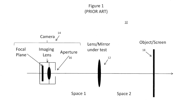
17 FIG. 1 is a schematic diagram illustrating a conventional Phase
Measuring =
18 Deflectometry system.
19 FIG. 2 is a schematic diagram illustrating additional features of the
conventional Phase Measuring Dellectometry system of FIG. 1.
21 FIG. 3 is a schematic diagram illustrating a system for measuring an
optical
22 system, in accordance with an exemplary embodiment of the present
disclosure.
23 FIG. 4 is a schematic diagram illustrating a system for measuring an
optical
24 system, in accordance with embodiments of the present disclosure.
FIG. 5 is a schematic diagram illustrating a system for measuring an optical
26 system, in accordance with embodiments of the present disclosure.
27 FIG. 6 is a schematic diagram illustrating a system for measuring an
optical
28 system, in accordance with embodiments of the present disclosure.
29 FIG. 7 is a schematic diagram illustrating a system for measuring an
optical
system, in accordance with embodiments of the present disclosure.
31 FIG. 8 is a schematic diagram illustrating a system for measuring an
optical
32 system, in accordance with embodiments of the present disclosure.
8
CA 02955391 2017-01-17
WO 2016/010670
PCT/US2015/036303
FIG. 9 is a schematic diagram illustrating a system for measuring an optical
2 system, in accordance with embodiments of the present disclosure.
3 FIG. 10 is a schematic diagram illustrating a system for measuring an
optical
4 system, in accordance with embodiments of the present disclosure.
FIG. 11 is a schematic diagram illustrating a system for measuring an optical
6 system, in accordance with embodiments of the present disclosure.
7 FIG. 12 is a schematic diagram illustrating a system for measuring an
optical
8 system, in accordance with embodiments of the present disclosure.
9 FIG. 13 is a schematic diagram illustrating a system for measuring an
optical
system, in accordance with embodiments of the present disclosure.
11 FIG. 14 is an illustration of various pupil types and characteristics
which may
12 - be utilized in embodiments provided by the present disclosure.
13 In the conventional Phase Measuring Deflectometry system 10, shown in
FIG.
14 1, the measurement is performed by mapping the rays from a space on one
side of the
optical system under test (e.g., lens/mirror 12), to the conjugate space on
the other
16 side of the optical system under test. In one space (space 1), an imager
such as a
17 digital camera 14 produces a series of images, mapping the rays through
some defined
18 pupil (e.g., aperture 16). In the other space (space 2), on the other
side of the optical
19 system under test 12, a pixilated screen 18 determines ray positions,
using shifted
sinusoidal patterns to determine phase on the screen 18. By imaging the screen
18
21 through the system under test 12, and observing the way the rays of
light from the
22 screen 18 are deviated, the system under test 12 can be measured.
23 One ray can be defined for each pixel on the imager 14, and its
conjugate pixel
24 on the screen 18 can be determined to some (generally, high) accuracy.
In describing
embodiments provided by the present disclosure, it is advantageous to first
define a
26 mathematical model for this conventional measurement system 10. The
following
27 notation is first defined, for a vector x, having some x,y coordinates,
at some specific
28 plane or space:
= (x,y),where z = zn
29 We then describe the test system 10 as mapping the first space,
conventionally
a plane, on one side of the optic, to the second space, or plane. As shown in
FIG. 2,
9
CA 02955391 2017-01-17
WO 2016/010670
PCT/US2015/036303
I we label one side Z, or image, and one side Zo, or object. At each plane,
we have
2 knowledge of the ray positions, at some resolution:
f =
3 We then construct the operator G, and its inverse. G operates on the
refractive
4 index variation n(x), where the refractive index variation is a model of
the optical
system under test, such as a lens 12. It will be readily appreciated, however,
that the
6 present invention is suitable for measuring optical elements and systems
that are
7 defined with other models.
8 The result of the operator G acting on the index variation n(x) is our
data, f(x),
9 the ray mapping. If we apply G inverse to our data, we get the refractive
index
variation. This simply states that we can conduct our Phase Measuring
Deflectometry
11 measurement and gain information about the optic being tested.
Summarized
12 mathematically, this is:
G n(x , y)} =f()
G {f (x,(:)1 = n(x, y)
13 We note, however, that n(x) must be two-dimensional, or quasi-two-
14 dimensional, as our mapping only has two degrees of freedom. This is a
significant
limitation of the conventional test, as, again, conventional Phase Measuring
16 Deflectometry can only measure a single surface, or the overall
transmitted
17 wavefront. It cannot separate, for example, the two surfaces of a lens.
This is, as the
18 above equations show, a fundamental limitation of the data.
19 The present invention overcomes this fundamental limitation of
conventional
Phase Measuring Deflectometry by obtaining more information during
measurement.
21 The present disclosure provides several methods for accomplishing this
objective. In
22 general, a full mapping of the rays on both sides of the optic under
test can be
23 obtained, and the accuracy and completeness of that measurement can be
improved.
24 FIG. 3 is a schematic diagram illustrating a system 30 for measuring an
optical
system which achieves the goal of providing full ray mapping, using multiple
imagers
26 34a, 34b in place of the single digital camera in the conventional
system of FIG. 1.
27 As shown in FIG. 3, an additional plane of resolution is added to the
system
28 30, a pupil plane, Zp. In the simplest case, with two cameras 34a, 34b,
this plane
CA 02955391 2017-01-17
WO 2016/010670
PCT/US2015/036303
1 offers two points of resolution, one for each camera pupil. High-
resolution
2 knowledge of the rays may thus be retained at the image and object plane.
3 The equation for the system's 30 ray-mapping is thus as follows:
f (.20),xzp') =
4 'Critically, this mapping now has additional information about the ray
paths,
from this added plane of resolution, the pupil plane. We can now write a model
of
6 our system 30, n(x), that includes depth, z, information.
G (n(x, y, z)) = f ("CZ, x
G-1 ff( )} = n(x, y, z)
7 The result of this is that the system 30, with three resolution planes,
can, for
8 example, separate errors in the first and second surfaces of a lens, or
measure the
9 index profile of a gradient index lens.
To be fully general, however, four planes of resolution may be required. FIG.
11 4 is a schematic diagram illustrating a system 40 for measuring an
optical system,
12 with four planes of resolution. In such a system 40, the ray angle and
direction must
13 be known both going into and leaving the optical system 12 being tested.
14 By making at least two measurements with the screen 18 displaced, or
with
two screens and a beam splitter, this can be achieved. Alternately, some
object48
16 may be inserted into a second pupil plane between the screen 18 and the
optic under
17 test 12. The system 40 model, with these two pupil planes (e.g., image
pupil and,
18 object pupil planes), now becomes:
f (x7), x7 = (x7), x
-pi Zp2
19 Using a fully general operator G, we can again define:
G-1 ft- n(x, y, z)
As full resolution is obtained at all four planes, n(x) becomes fully general,
21 and can have any sort of Z information. Because any optical system's ray-
22 propagation can be measured, the measurement systems and methods
provided herein
23 are termed FORM (Flexible Optical Ray Metrology).
24 The present disclosure provides several systems and methods for creating
these four planes of resolution. Resolution at the image, and on the object,
can
11
CA 02955391 2017-01-17
WO 2016/010670
PCT/US2015/036303
1 generally be created using a CMOS or CCD detector (e.g, camera 34a, 34b)
and an
2 LCD screen (e.g., screen 18), respectively. Resolution in the image pupil
plane may
3 be created utilizing several systems and methods, including the systems
shown in
4 FiGs. 5 through 9 herein.
FIG. 5 is a schematic diagram illustrating a system 50 for measuring an
optical
6 system, in accordance with an exemplary embodiment of the present
disclosure. The
7 system 50 includes multiple detectors (e.g., 34a, 34b), each having
different angles of
incidence (e.g., angle #1., angle #2), thus providing resolution in the image
pupil
9 plane.
FIG. 6 is a schematic diagram illustrating a system 60 for measuring an
optical
11 system, in accordance with another embodiment of the present disclosure.
The
12 system 60 includes a detector 64 having a lenslet array 65, thus
providing resolution
13 in the image pupil plane.
14 FIG. 7 is a schematic diagram illustrating a system 70 for measuring an
optical
system, in accordance with another embodiment of the present disclosure. The
16 system 70 includes one or more detectors 34a, 34b, each positioned at
different
17 depths, or Z distances (distance #1, distance #2), thus providing
resolution in the
18 image pupil plane.
19 FIG. 8 is a schematic diagram illustrating a system 80 for measuring an
optical
system, in accordance with another embodiment of the present disclosure. The
21 system 80 includes one or more detectors 84a, 84b with a Hartmann screen
or array
22 85a, 85b, thus providing resolution in the image pupil plane.
23 FIG. 9 is a schematic diagram illustrating a system 90 for measuring an
optical
24 system, in accordance with another embodiment of the present disclosure.
The
system 90 includes one or more detectors 34a, 34b which are scanned in angle
(e.g.,
26 scan angles #1 and #2, as shown in FIG. 9) or scanned in position, thus
providing
27 resolution in the image pupil plane.
28 Further, resolution in the object pupil plane may be created utilizing
various
29 systems and methods, including the systems shown in FIGs. 10 through 13
herein.
FIG. 10 is a schematic diagram illustrating a system 100 for measuring an
31 optical system, in accordance with another embodiment of the present
disclosure. The
12
CA 02955391 2017-01-17
WO 2016/010670 PCT/US2015/036303
1 system 100 includes a single screen 18, which is scanned in the Z
direction, or depth,
2 thus providing resolution in the object pupil plane.
3 FIG. 11 is a schematic diagram illustrating a system 110 for measuring
an
4 optical system, in accordance with another embodiment of the present
disclosure. The
system 110 includes a plurality of screens 18a, 18b, each at different Z
distances
6 (distance #1, distance #2), optically coupled with a beamsplitter 111,
thus providing
7 resolution in the image pupil plane.
8 FIG. 12 is a schematic diagram illustrating a system 120 for measuring
an
9 optical system, in accordance with another embodiment of the present
disclosure. The
system 120 includes an aperture 126 or series of apertures in the object pupil
plane,
11 which may be scanned in the X and/or Y directions, thus providing
resolution in the
12 image pupil plane.
13 FIG. 13 is a schematic diagram illustrating a system 130 for measuring
an
14 optical system, in accordance with another embodiment of the present
disclosure. The
system 130 includes a grating 136 positioned in the object pupil plane, which
may. be
16 moved or phase shifted in the X and/or Y directions, thus providing
resolution in the
17 image pupil plane.
18 As will be understood by those skilled in the relevant art, the systems
and
19 methods provided herein for providing resolution in the image pupil
plane (e.g., as
shown in FIGs. 5 through 9) may be combined with those for providing
resolution in
21 the object pupil plane (e.g.; as shown in FIGs. 10 through 13), as
desired, so that
22 partial or full resolution may be created at one or both pupil planes
(i.e., the image
23 pupil plane and the object pupil plane). Moreover, it will be readily
understood by
24 those skilled in the relevant art that partial or full resolution may be
created at
additional planes utilizing various combinations of the systems and methods
provided
26 herein. All such combinations are intended to be included herein within
the scope of
27 this disclosure.
28 It should be noted that although the analogy of rays is used with
respect to the
29 measurement systems provided herein, rays are non-physical.
Fundamentally, the
wave nature of light is apparent in the data. Thus, there is no loss of
generality, and
31 wave-optics phenomena such as diffraction may be observed. In
particular, a ray
32 analysis would seem to require continuous surfaces for measurement.
However,
13
CA 02955391 2017-01-17
WO 2016/010670
PCT/US2015/036303
1 because measurements in accordance with the disclosure are wave-optics
tests,
2 discontinuities in surface sag or slope may be accurately measured.
3 The present disclosure thus enables measurement of both surfaces of a
lens or
4 optical system under test, a significant advantage over conventional
measurement
techniques. Furthermore, the present disclosure facilitates improved accuracy
and
6 resolution of the data. Noting again that wave-optics phenomena are
significant, the
7 details and characteristics of each pupil in the pupil planes (e.g.,
image and object
8 pupil planes) are significant with respect to accuracy and resolution.
For the camera
9 or image pupil, there are advantages provided by comparatively large and
small
pupils. A large pupil allows more light to be collected, and, due to
diffraction, creates
ti a smaller image at the surface being tested, allowing for higher
resolution.
12 A smaller pupil, by contrast, creates more diffraction, reducing
resolution at
13 the surface being tested, but creating more well-defined rays, allowing
small slopes
14 with big extents to be accurately measured, and reducing the effects of
certain
systematic errors. This greater diffraction also allows discontinuities to be
measured
16 more effectively.
17 Other sorts of pupils besides simply large and small may be considered
and
18 utilized in any of the systems and methods provided herein. FIG. 14
illustrates a
19 variety of pupil types and features which may be utilized. For example,
non-circular
stops may be utilized, such as slits, crossed slits; and groups or gratings of
slits. Pairs
21 or arrays of circular or non-circular holes may also be utilized. Each
of these offers
22 tradeoffs of resolution and diffraction behavior.
23 Similarly, various optical elements may be placed in the pupil planes
and
24 utilized in any of the systems and methods provided herein. Polarizers,
waveplates,
spatial light modulators and the like may be introduced in a pupil plane to
allow
26 polarization behavior to be studied. Color filters, gratings and prisms
may be
27 introduced to allow color information to be captured. With the right
combination of
28 elements, the full wave nature of light may be interrogated for the
system being
29 tested.
These various pupil features and sizes may be combined, and different pupils
31 assigned to each camera, or the pupil may be varied at different times
during the
32 measurement. By doing so, the accuracy of the measurement may be
improved, so
14
CA 02955391 2017-01-17
WO 2016/010670
PCT/US2015/036303
1 that both very large- and small-scale features may be accurately
measured,- including
2 discontinuities. Additional information may also be obtained about
polarization and
3 color effects of the optical system being tested.
4 The systems and methods provided herein may include an electronic
computer
for controlling the measurement process and/or receiving and analyzing the
results of
6 such measurements, including any such computer systems for controlling
7 measurements of optical systems as may be known within the relevant
field. The
8 computer may be utilized in the present invention, for example, to
coordinate the
9 modulation of the optical source and/or masks and the image acquisition
by the
sensors. The computer may further determine the mapping relations (e.g.,
between
11 points on the optical system and corresponding geometric locations of
points in the
12 diffuse optical source), and determine properties of the optical system.
13 Moreover, it will be appreciated that the present invention enables a
14 calibration of errors in one or more of the sensors to be determined
based on the
mapping relations for each of the sensors, as well as in the optical source.
16 The systems and methods provided herein may be utilized to determine
17 various properties of the optical systems or surfaces under test,
including a
18 measurement of both surface shapes for a refractive optic or for
measuring a specular
19 surface.
In some embodiments, systems and methods provided herein may perform a
21 measurement of an optical system by measuring a first portion of the
optical system
22 while the optical system is in a first position and then measuring a
second portion of
23 the optical system while the optical system is in a second position. A
measurement of
24 the full optical system is then generated by combining the measurements
of the first
and second portions.
26 Similarly, the position of the optical system may be rotated, thereby
enabling
27 measurement of optical systems having an angular acceptance too large
for measuring
28 in a single measurement.
29 It should be emphasized that the above-described embodiments of the
present
disclosure, particularly, any "preferred" embodiments, are merely possible
examples
31 of implementations, merely set forth for a clear understanding of the
principles of the
32 disclosure. Many variations and modifications may be made to the above-
described
CA 02955391 2017-01-17
WO 2016/010670
PCT/US2015/036303
embodiment(s) of the disclosure without departing substantially from the
spirit and
2 principles of the disclosure. All such modifications and variations are
intended to be
3 included herein within the scope of this disclosure and the present
disclosure and
4 protected by the following claims.
16