Note: Descriptions are shown in the official language in which they were submitted.
CA 02955789 2017-01-19
WO 2016/019011
PCT/US2015/042649
LIGHT EMITTING DIODE RETROFIT LAMP FOR HIGH INTENSITY DISCHARGE
BALLAST
TECHNICAL FIELD
10001] The present invention relates generally to light emitting diode
(LED) lamps. In
particular, the present invention relates a LED retrofit lamp for a high
intensity discharge
(HID) ballast.
BACKGROUND
[0002] A HID lamp is an arc-type lamp which produce light by forming an
electric arc
between electrodes housed in a fused alumina arc tube or transparent fused
quartz filled with
gas and metal salts. Once the arc is started using the gas, the metal salts
are evaporated to
form a plasma. The HID lamp converts input electrical energy into light energy
by using
input electrical energy to increase the energy in the plasma, producing light
based on the
collision of electrons and ions with neutral metal atoms.
[0003] FIG. 1 illustrates an example of a conventional HID lamp 10 having
an outer
ellipsoidal-shaped bulb 12 including an internal phosphor coating 14. The HID
lamp 10
further includes an arc tube 16 connected to a support structure 18. A
starting resistor 20 is
connected with a starting electrode 22 for initiating the arc. A lower end of
the bulb 12 is
seated within a cap 24 for connecting to a power source. A ballast is used to
operate the HID
lamp 10.
[0004] In LED applications, light is generated more efficiently than in the
HID
applications. Light is generated when a conduction band electron re-combines
with a hole in
a valance band of the semiconductor. The semiconductor is created by doping a
di electic
therein with donor (n-type) or acceptor (p-type) atoms. The LED is created by
a sandwich of
the n-type and p-type materials, such that the energy drop from conduction to
valance band is
equal to the energy of the light emitted (i.e., desired frequency or
wavelength).
[0005] The LED is a structure that includes free electrons and holes such
that when an
electric field is applied across it, energy is transferred to the electrons
and the holes more
directly by increasing the drift velocity. Thus, more electrons can make the
transition from
the valence band to the conduction band, creating holes, and the electrons
therefore
1
CA 02955789 2017-01-19
WO 2016/019011
PCT/US2015/042649
recombine with holes generating a desired radiation.
III. Summary of the Embodiments
[0006] Embodiments of the present invention provide a LED retrofit lamp for
an HID
ballast and a method for replacing an existing HID lamp with the LED retrofit
lamp and
interfacing an LED driver with the existing HID ballast.
[0007] In one exemplary embodiment, an LED retrofit lamp interfacing with a
HID
ballast is provided. LED retrofit lamp includes a lighting source comprising a
plurality of
LEDs, one or more heat sink components dissipating heat generated by the LEDs,
and an
LED driver configured to operate the LEDs. The LED retrofit lamp is disposed
within an
HID housing and the HID ballast is electrically connected with the LED driver,
and supplies
power to the LED driver for operating the LEDs.
[0008] According to yet another exemplary embodiment, a method is provided.
The
method includes disposing a LED retrofit lamp into an existing HID lamp
housing,
electrically connecting an LED driver of the LED retrofit lamp with the
existing HID ballast,
supplying output voltage from the HID ballast to the LED driver, and
regulating the output
voltage and operating LEDs of the LED retrofit lamp using the regulated DC
output voltage,
[0009] The foregoing has broadly outlined some of the aspects and features
of various
embodiments, which should be construed to be merely illustrative of various
potential
applications of the disclosure. Other beneficial results can be obtained by
applying the
disclosed information in a different manner or by combining various aspects of
the disclosed
embodiments. Accordingly, other aspects and a more comprehensive understanding
may be
obtained by referring to the detailed description of the exemplary embodiments
taken in
conjunction with the accompanying drawings, in addition to the scope defined
by the claims.
BRIEF DESCRIPTION OF THE DRAWINGS
[0010] FIG. l is a schematic illustrating an example of a HID lamp.
[0011] FIG. 2A and 2B are schematics each illustrating an LED retrofit lamp
that can be
implemented within one or more embodiments of the present invention.
[0012] FIG. 3 is an exploded view of the LED retrofit lamp shown in FIG.
2B.
2
CA 02955789 2017-01-19
WO 2016/019011
PCT/US2015/042649
[0013] FTG. 4 is a schematic illustrating the LED retrofit lamp disposed
within an
existing HID lamp housing that can be implemented within one or more
embodiments of the
present invention.
[0014] FIG. 5 is a circuit schematic illustrating the electrical connection
between a HID
ballast and a LED driver in accordance with one or more embodiments of the
present
invention.
[0015] FIG. 6 is a circuit schematic illustrating a HID voltage control
circuit that can be
implemented within one or more embodiments of the present invention.
[0016] FIGS. 7A and 7B are schematics illustrating LED retrofit lamps
according to one
or more alternative embodiments of the present invention.
[0017] FIG.8 is a graph illustrating the optical distribution of the LED
retrofit lamp
according to one or more embodiments of the present invention.
[0018] FIG. 9 is a flow diagram for a method replacing an existing HID lamp
with the
LED retrofit lamp and interfacing an LED driver with the existing HID ballast
that can be
implemented within one or more embodiments of the present invention.
[0019] The drawings are only for purposes of illustrating preferred
embodiments and are
not to be construed as limiting the disclosure. Given the following enabling
description of
the drawings, the novel aspects of the present disclosure should become
evident to a person
of ordinary skill in the art. This detailed description uses numerical and
letter designations to
refer to features in the drawings. Like or similar designations in the
drawings and description
have been used to refer to like or similar parts of embodiments of the
invention.
DETAILED DESCRIPTION
[0020] As required, detailed embodiments are disclosed herein. It must be
understood
that the disclosed embodiments are merely exemplary of various and alternative
forms. As
used herein, the word "exemplary" is used expansively to refer to embodiments
that serve as
illustrations, specimens, models, or patterns. The figures are not necessarily
to scale and
some features may be exaggerated or minimized to show details of particular
components. In
other instances, well-known components, systems, materials, or methods that
are known to
those having ordinary skill in the art have not been described in detail in
order to avoid
3
CA 02955789 2017-01-19
WO 2016/019011
PCT/US2015/042649
obscuring the present disclosure. Therefore, specific structural and
functional details
disclosed herein are not to be interpreted as limiting, but merely as a basis
for the claims and
as a representative basis for teaching one skilled in the art.
[0021] Embodiments of the present invention provide an LED retrofit lamp
for HID
lamps and a method for interfacing an LED driver with an existing HID ballast.
Details
regarding the LED retrofit lamp are described below with reference to FIGS.
2A, 2B and 3.
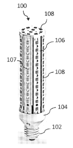
[0022] FIG. 2A and 2B are schematics each illustrating an LED retrofit lamp
100, 200
that can be implemented within one or more embodiments of the present
invention. As
shown in FIG. 2A, the LED retrofit lamp 100 includes a base 102, a cap portion
104, a
printed circuit board (PCB) 106 including openings 107 therein. LEDs 108 are
mounted to
and thermally connected with the PCB 106, to allow more efficient transfer of
heat from the
LEDs 108 to the ambient air.
[0023] The LED's 108 can be mounted in a linear pattern on the PCB 106, as
shown in
FIGs. 2A and 2B. This linear pattern extends along a same length as that of an
arc-length of
a standard HID lamp, and thereby more closely mimic the optical distribution
of the HID
lamp, as shown in FIG.8.
[0024] Referring to FIG. 8, as shown in the graph 800, when LEDs 108 are
not formed
on top of the LED retrofit lamp 100 (see arrow 802), the LEDs 108 produce
light at a smaller
distance compared to when the LEDs 108 are formed on top of the LED retrofit
lamp 100
(see arrow 804)
[0025] The openings 107 are formed between the LEDs 108 and allow air flow
between
the LED 108s, for enhanced cooling. As shown in FIG. 2B, the LED retrofit lamp
200
includes all the elements of LED retrofit lamp 100 including a base 202, a cap
portion 204, a
PCB 206 including openings 207 and LEDs 208 mounted on the PCB 206. The LED
retrofit
lamp 200 further includes a heat sink 212 having a plurality of heat sink
components (e.g.,
fins) 214, for better thermal management.
[0026] The heat sink fins 214 are formed in a "tulip" shape, however the
present
invention is not limited hereto and may vary accordingly. The heat sink fins
214 enhance the
radiative and convective heat dissipation. The heat sink fins 214 may be
formed of a
4
277089
composite structure out of a plurality of predominantly parallel, axially
oriented carbon fibers
that have been laminated to an underlying material such as a thermo-formable
plastic.
[0027] A thermal conduction path would be formed from a rear side of the
PCB 206 and
would be axially along the carbon fibers which are oriented perpendicular to
the optical axis
of the lamp. The heat is transmitted along the carbon fibers allowing for
convective heat
transfer to the environment. The heat sink fins 214 may be formed comparable
to that
disclosed in the Application entitled Crystalline-Graphic-Carbon-Based Hybrid
Thermal
Optical Element for Lighting Apparatus by Gary Allen et al.
[0028] The LED retrofit lamps 100, 200 are supplied power by an LED driver
(as
depicted in FIG. 3). FIG. 3 is an exploded view of the LED retrofit lamp 200
shown in FIG.
2B. The LED driver 220 is housed within a hollow region 215 of the heat sink
212. LEDs
208 are disposed in the top surface and side surfaces of the LED retrofit lamp
200 to further
enhance the illumination and light distribution of the lamp 200. The LED
driver 220 includes
various electrical components for driving the LEDs 208. Details regarding the
LED driver
220 will be discussed below with reference to FIG. 5.
[0029] In accordance with the embodiments, the LED retrofit lamp 100 or 200
is fitted
within an existing HID lamp housing 300 (e.g., the HID outer bulb) as shown in
FIG. 4. For
the purposes of illustration only, the LED retrofit lamp 200 is shown fitting
within the HID
lamp housing 300. As shown the LED retrofit lamp 200 interfaces seamlessly
with the
existing HID lamp housing 300. The LED driver 220 shown in FIG. 3 interfaces
with the
HID ballast associated with the existing HID lamp housing 300.
[0030] Details regarding the electrical connection between the LED driver
220 and the
HID ballast will now be discussed with reference to FIG. 5.
[0031] FIG. 5 is a schematic illustration of the electrical connection
between a HID
ballast 320 and a LED driver 400 in accordance with one or more embodiments of
the present
invention. As shown in FIG. 5, the HID ballast 320 is a choke ballast however
the present
invention is not limited hereto and may be applied to all types of HID
ballasts. The HID
ballast 320 includes an AC input 310 for receiving AC power from an AC power
supply, and
outputs 330 and 332 of the HID ballast 320 are connected with the LED driver
400.
CA 2955789 2018-05-29
CA 02955789 2017-01-19
WO 2016/019011
PCT/US2015/042649
[0032] Output 330 is connected to a bridge rectifier 402 of the LED driver
400 via a fuse
334. The output 332 is connected directly to the bridge rectifier 402, via
fuse 334. The
bridge rectifier 402 includes a plurality of diodes for delivering a rectified
voltage (e.g., DC
voltage) to the LED driver 400. The bridge rectifier 402 is connected with a
buck circuit 404
for lowering the DC output of the bridge rectifier 402 to a desired DC output
for LEDs 408.
[0033] The LEDs 408 are representative of the LEDs 108 and 208 of the LED
retrofit
lamps 100, 200 shown in FIGs. 2A and 2B. The buck circuit 404 includes a
capacitor 409
and a voltage divider 410. The rectified voltage is filtered by the capacitor
409, and applied
across the voltage divider 410.
[0034] The buck circuit 404 further includes a switch controller 420 which
is an
integrated circuit (IC) that receives a plurality of electrical signals at a
plurality of input pins
thereof The switch controller 420 also provides a switch signal to the
converting switch
430. The input pins include, for example, a DRIVE pin 1, CS pin 2, BOS pin 3,
Ground
(GND) pin 4, DIM pin 5, NC pin 6, VCC pin 7 and TEST pin 8. The switch
controller 420 is
not limited to a particular type of switch controller and therefore include
any switch
controller suitable for the purpose set forth herein.
[0035] The controller supply voltage, Vcc, is applied to the switch
controller 420 at the
Vcc pin 7 and is used to power the switch controller 420. The converting
switch 430 is
coupled with the DRIVE pin 1 such that a gate of the converting switch 430 is
controlled by
the DRIVE pin 1 of the switch controller 420. The converting switch 430 is
coupled with an
inductor 440 and when the converting switch 430 is closed, the inductor is
connected to
ground via resistor 442, forming a controlled power switch path for charging
and discharging
the inductor 440. The buck circuit 404 further includes a diode 444 and two
output
capacitors 450 and 452.
[0036] When the converting switch 430 is switched ON, it is supplying the
LED load
(i.e., LEDs 408) with current. Initially current flow to the LED load (LEDs
408) is restricted
as energy is also being stored in the inductor 440, therefore the current in
the LED load and
the charge on the output capacitors 450,452 builds up gradually during the
'ON' period.
Throughout the ON period, there will be a large positive voltage on the
cathode of the diode
444, therefore the diode 444 will be reverse biased and therefore play no part
in the action.
When the converting switch 430 switches off, the energy stored in the magnetic
field around
6
CA 02955789 2017-01-19
WO 2016/019011
PCT/US2015/042649
the inductor 440 is released back into the circuit. The voltage across the
inductor 440 is then
in reverse polarity to the voltage across the inductor 440 during the 'ON'
period, and
sufficient stored energy is available in the collapsing magnetic field to keep
current flowing
for at least part of the time the converting switch 430 is open. The inductor
440 now causes
current to flow around the circuit via the LED load and the diode 444, which
is now forward
biased. Once the inductor 440 has returned a large part of its stored energy
to the circuit and
the load voltage begins to fall, the charge stored in the output capacitors
450,452 becomes the
main source of current, keeping current flowing through the LED load until the
next 'ON'
period begins.
[0037] By way of example, the HID ballast 320 may be an electromagnetic
ballast or an
electronic ballast. When the HID ballast 320 is an electromagnetic ballast, it
may include
ignitor. If the HID ballast 320 includes an ignitor, HID voltage control
circuit 600 shown in
FIG. 6 is implemented to clamp a pulse of the ignitor to a predetermined
acceptable level,
prior to transmitting the voltage to the LED driver 400.
[0038] The circuit 600 includes a plurality of resistors R1, R2, R3 and R4
and a bi-
directional transient voltage suppressor (TVS) diode bridge 610 to eliminate
transient
voltages (i.e., unwanted spikes or surges) from the HID ballast 320 from being
transmitted to
the LED driver 400.
[0039] The present invention provides several ways to enhance thermal
management of
the LED retrofit lamps 100, 200 shown in EEGs. 2A and 2B. These additional
aspects will
now be described below with references to FIGS. 2A, 2B, 7 and 8.
[0040] Referring back to F1Gs. 2A and 2B, as previously mentioned, the PCBs
106 and
206 may include openings 107, 207 for further enhancing heat dissipation of
the LEDs 108
and 208. Further, as shown in FIG. 2B, the heat sink 212 enables the
dissipation of additional
heat from the LEDs 108 and 208 through the PCBs 106 and 206. The heat sink
fins 214 of
the heat sink 212 may be formed of one or more material layers including a
thermally
conductive material and a high reflective material.
[0041] As shown in FIG. 7A, the openings 207 may be larger than that shown
in FIG. 2B,
for better air flow to thereby further enhance heat dissipation the LEDs 108.
Further, the heat
sink fins 214 may be coated with a protective coating layer (e.g., a first
protective layer 700)
7
CA 02955789 2017-01-19
WO 2016/019011
PCT/US2015/042649
including, for example, a conformal coating or gels, or a matte finish
coating, a white
reflective coating or clear coating to provide a hard scratch abrasion type
surface and
electrical insulation. The conformal coating or gels cure in place, to form a
resilient
protective layer on the heat sink surface. This layer can also provide
electrical isolation.
[0042] As depicted in FIG. 7B, the heat sink fins 214 may be coated with
the first
protective coating layer 700 and the LEDs 208 may be coated with a second
protective
coating layer 702. The second protective coating layer 702 may be formed of
the same
material as that of the first protective coating layer 700 or of a different
material. For
example, the second protective coating layer 702 may be an organic
polysilazane coating to
enable to LEDs 208 exposed without need for any additional protective coating.
Another
form of this protective layer can be a transparent hard plastic material such
as polymethyl
methacrylate (PMMA) or polycarbonate shield. In other embodiments, the LED
retrofit
lamps 100 and 200 may further include a fan to drive more heat transfer from
the LEDs 108
and 208 to the ambient air.
[0043] FIG. 9 is a flow diagram illustrating an exemplary method of
replacing an existing
HID lamp with the LED retrofit lamp and interfacing an LED driver with the
existing HID
ballast that can be implemented within one or more embodiments of the present
invention.
As shown in FIG. 9 with reference made to FIGs. 4 and 5, the method 900 begins
at operation
910 where an LED retrofit lamp 200 is disposed within a HID lamp housing 300.
[0044] From operation 910, the process continues to operation 920 where the
existing
HID ballast 320 is electrically connected with the LED driver 400. During
operation, at
operation 930, input voltage received at the HID ballast 320 is transmitted to
the LED driver
400. At operation 940, a bridge rectifier 402 of the LED driver 400 rectifies
the voltage
received and transmits the voltage to a buck circuit 404 connected thereto. At
operation 950,
the buck circuit 404 lowers the voltage to a predetermined acceptable level
for operating the
LEDs 208 of the LED retrofit lamp.
[0045] As noted above, if the HID ballast 320 includes an ignitor, the
ignitor pulse is
controlled via a HID voltage control circuit 600 between the HID ballast 320
and the input to
the LED driver 400, to protect the LED driver 400 from any undesired voltage
(e.g., voltage
surges or spikes).
8
277089
[0046] Embodiments of the present invention provide the advantages of
utilizing an
existing HID envelope and ballast and adding the light generation method of an
LED retrofit
lamp disposed within the existing HID envelope using the LED driver in
electrical
communication with the HID ballast.
[0047] This written description uses examples to disclose the invention,
including the
best mode, and also to enable any person skilled in the art to practice the
invention, including
making and using any devices or systems and performing any incorporated
methods. The
patentable scope of the invention may include other examples that occur to
those skilled in the
art in view of the description. Such other examples are intended to be within
the scope of the
invention.
9
CA 2955789 2018-05-29