Note: Descriptions are shown in the official language in which they were submitted.
CA 02955832 2017-01-19
WO 2016/044190
PCT/US2015/050053
PROCESSOR VALIDATED WAKEUP SYSTEM AND METHOD
CROSS-REFERENCE TO RELATED APPLICATIONS
This application claims the benefit of U.S. Provisional Patent Application No.
62/050,487 filed September 15, 2014, the contents of which are incorporated
herein by
reference in their entirety.
BACKGROUND OF THE INVENTION
1. Field of the Invention
The present invention relates generally to wireless networks and in particular
to power
management for wireless networks.
2. Description of Related Art
Wireless networks may be used to transmit signals to devices that are
activated
intermittently. For example, a wireless signal may be used to lock or unlock a
door leading to
a house or hotel room. Most often, the circuitry within the locking device is
in a sleep mode
until triggered by a wakeup signal. Preserving power within the device during
periods of
nonuse is traditionally limited by the ability to put the system of the device
into lower power
sleep modes. Traditionally, there exist systems for managing power consumption
of the
device which make it available to receive external requests. For example, a
receiver of the
device may power up on a schedule and check for signals. This scheduling
approach allows
the receiver to be shut down most of the time and conserve battery power.
There are at least
two limitations with this method. First, the receiver is still being powered-
up at certain
intervals which can require the use of critical battery power. Second, some
wireless networks
require acquisition time for the network to synchronize and verify security
protocols, and the
like. This can be a time consuming process and by correlation, a power
consuming process.
1
CA 02955832 2017-01-19
WO 2016/044190
PCT/US2015/050053
Such conventional methods and systems have generally been considered
satisfactory
for their intended purpose. However, there is still a need in the art for
improved power
management for wireless networks. The present disclosure provides a solution
for this need.
2
CA 02955832 2017-01-19
WO 2016/044190
PCT/US2015/050053
SUMMARY OF THE INVENTION
A system includes a transceiver for receiving a wake up signal from a wireless
communication device. A processor is operatively connected to the transceiver
and to a
memory. The memory includes instructions recorded thereon that, when read by
the
processor, cause the processor to transition from a sleep mode to an active
mode and to
power up the transceiver upon validation of the wake up signal.
The processor can analyze a pulse of the wake up signal to determine if the
wake up
signal is valid such that the processor can be fully activated if the wake up
signal is valid. The
processor can return to sleep mode if the wake up signal is invalid.
The transceiver can receive an RF wake up signal from an RF source such as a
smart
phone. The system can also include an RF detector for converting the RF wake
up signal to
DC pulses to be evaluated by the processor.
A method for transitioning a system from a sleep mode to an active mode
includes
receiving a wake up signal from a wireless communication device at a
transceiver. The wake
up signal is validated through a processor. The processor wakes from a sleep
mode upon
validation of the wake up signal.
A system for providing access to a locked device comprises a locking mechanism
configured to selectively switch between a locked state and an unlocked state.
A wireless
interface is operatively connected to the locking mechanism to control change
between the
locked and unlocked states. The wireless interface is configured to receive a
wake up signal
from a wireless communication device at a transceiver and validate the wakeup
signal
through a processor. Upon validation the processor activates the locking
mechanism.
3
CA 02955832 2017-01-19
WO 2016/044190
PCT/US2015/050053
These and other features of the systems and methods of the subject disclosure
will
become more readily apparent to those skilled in the art from the following
detailed
description of the preferred embodiments taken in conjunction with the
drawings.
4
CA 02955832 2017-01-19
WO 2016/044190
PCT/US2015/050053
BRIEF DESCRIPTION OF THE DRAWINGS
So that those skilled in the art to which the subject disclosure appertains
will readily
understand how to make and use the devices and methods of the subject
disclosure without
undue experimentation, preferred embodiments thereof will be described in
detail herein
below with reference to certain figures, wherein:
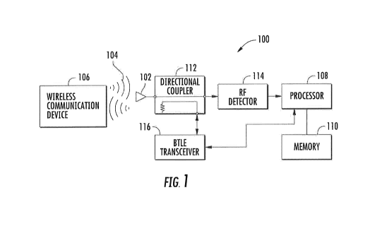
Fig. 1 is a schematic view of an exemplary embodiment of a system for
validating a
wakeup signal constructed in accordance with the present disclosure, showing a
transceiver
and a processor;
Fig. 2 is a flow chart showing an exemplary embodiment of a method for
validating a
wakeup signal using the system of Fig. 1;
Fig. 3 is a schematic view of an exemplary RF passive wakeup circuit of the
processor
of Fig. 1; and
Fig. 4 is a schematic view the system of Fig. 1 used with an exemplary
embodiment
of a locking mechanism.
5
CA 02955832 2017-01-19
WO 2016/044190
PCT/US2015/050053
DETAILED DESCRIPTION OF THE PREFERRED EMBODIMENTS
Reference will now be made to the drawings wherein like reference numerals
identify
similar structural features or aspects of the subject disclosure. For purposes
of explanation
and illustration, and not limitation, a partial view of an exemplary
embodiment of a system
for validating a wake up signal in accordance with the disclosure is shown in
Fig. 1 and is
designated generally by reference character 100. Other embodiments of systems
and
methods in accordance with the disclosure, or aspects thereof, are provided in
Figs. 2-4, as
will be described.
Fig. 1 illustrates a system 100 in accordance with the present disclosure for
validating
a wake up signal. As will be described in further detail, the system 100
achieves low sleep
current during nonuse thereby preventing unnecessary power consumption within
the system.
The system 100 includes an antenna 102 for receiving a wakeup signal 104 from
a wireless
communication device 106. The system 100 takes advantage of automatic
transmissions that
are emitted from the wireless communication device 106 when the device 106
initiates
contact with the system 100. The wireless communication device 106 can be a
smartphone or
any other type of Bluetooth wireless device which transmits an RF signal. To
reduce
unnecessary power consumption, the RF signal received by the antenna 102 is
passively
received through a non-powered, low loss directional coupler 112 to a non-
powered and
efficient RF detector 114. The RF detector 114 receives the RF wake signal and
converts the
RF wakeup signal to DC pulses which is received by a processor 108 connected
thereto. To
further conserve power, the processor 108 is in a deep sleep until the DC
pulses are received.
When the processor 108 receives the DC pulses, the processor reads from a
specific location
in a memory 110 operatively connected to the processor. The memory contains
further
instructions and wakeup validation criteria that enable the processor 108 to
transition from a
deep sleep mode to an active mode if all validation steps are passed. More
specifically, the
6
CA 02955832 2017-01-19
WO 2016/044190
PCT/US2015/050053
processor 108 evaluates the wake up signal 104 and if the signal is valid, the
processor 108
remains awake. Once the processor is fully awakened by a valid wakeup signal,
the processor
powers up the remaining components 112, 114, 116 of the system100. A BTLE
transceiver
116 operatively connected to the directional coupler 112 establishes a link
with the device
106. Through the directional coupler 112 and antenna 102, the BTLE transceiver
116
communicates to the wireless communication device 106 that the wakeup signal
104 has been
validated and prompts a user of the device to enter an access code, for
example, to
lock/unlock a door.
With reference to Fig. 2, a method 200 of validating a wake up signal is
shown. A
wireless communication device, e.g., wireless communication device 106,
transmits an RF
wakeup signal at box 202. The RF wakeup signal can be generated through any
suitable
technique. For example, an application stored on the wireless communication
device, once
activated, can cause the wireless communication device to transmit the RF
signal. Next, the
wake up signal is received at an antenna, e.g., antenna 102, at box 204. The
wakeup signal is
directed to an RF detector, e.g., RF detector 114, through a directional
coupler, e.g.,
directional coupler 112. The RF detector converts the RF signal to DC pulses,
as shown at
box 206, so that the signal is read as DC pulses by a processor, e.g.,
processor 108. The
processor partially awakes from a sleep mode once the processor detects the
received DC
pulses. The processor validates the DC pulses by analyzing the time between
pulses, at box
208. If the pulse shape, e.g., the timing, is correct, the processor exits
sleep mode and remains
awake, as shown at box 210, however, if the processor determines the pulse
shape is incorrect,
the processor does not exit sleep mode, but instead returns to a deep sleep
mode, as shown at
box 212. In the deep sleep mode, the processor can remain completely inactive
until partially
awakened by the next DC signal from the RF detector.
7
CA 02955832 2017-01-19
WO 2016/044190
PCT/US2015/050053
In this manner, the processor 108 follows a two-step approach to determine if
the RF
wake up signal 104 is valid. First, the directional coupler and RF detector
uses passive analog
verification of the RF wakeup signal. During this time the processor is
polling an interrupt
pin looking for certain DC voltage. If the analog section filter passes, the
DC voltage rises
enough to trip the processor to wake from deep sleep. The processor requires
very little
power to partially awaken from a sleep mode and even less while monitoring its
interrupt port.
Second, the DC pulses of the passive signal are analyzed using digital
processing in the
processor to determine if the wake up signal 104 is valid. With reference to
Fig. 3, a
schematic view of an exemplary embodiment of a circuit 300 for system 100 is
shown
illustrating the detailed connection between the BTLE transceiver 116, the
directional coupler
112 and the RF detector 108. The RF detector is operatively connected to the
processor 108
to send the DC pulses thereto. The antenna is 102 is operatively connected to
the directional
coupler 112 to send and receive signals.
The system 100 can be operatively connected to a locking mechanism 420 as
shown
in Fig. 4. Once the processor 108 is awakened by the wake up signal 104, as
described above,
the system verifies additional criteria, if needed, to activate the locking
mechanism 420 and
provide access, e.g., for a guest to enter a hotel room using a wireless
device. System 100
maintains low power consumption during nonuse to conserve power so that
locking
mechanism 420 can operate on battery power. The locking mechanism is a lock
420 on a
door, for example, a door to a hotel room or a door of a house, etc. The lock
420 can switch
between a locked state and an unlocked state to allow a user entry/exit. A
wireless interface
430 is operatively connected to the lock 420 to control change between the
locked and
unlocked states. The wireless interface 430 includes system 100. A user
attempting to lock or
unlock the door transmits the RF wake up signal 104 from the wireless
communication
device 106. Processor 108 of system 100 validates the wake up signal 104. If
the wake up
8
CA 02955832 2017-01-19
WO 2016/044190
PCT/US2015/050053
signal 104 is valid, the BTLE transceiver 116 prompts the user to enter an
access code 426
into the wireless communication device 106. The access code 426 is received by
the antenna
102 of system 100 and is passed through the directional coupler 112 and
received by the
BTLE transceiver 116 now in a receive mode. The BTLE transceiver demodulates
the access
code 426 and the access code 426 is presented to the processor 108 for memory
110
verification. The processor 108 using the memory 110 compares this code with a
stored code.
If the access code 426 is valid, i.e., if a match between the access code and
stored code is
found, processor 108 proceeds to send a lock/unlock signal to the locking
mechanism 420
through motor driver circuitry (not shown).
In this manner, a wireless communication device can be used to transmit a
wireless
wake up signal to lock or unlock the door. Further, as the processor only
remains awake upon
validation of the wake up signal, the power consumption in the wireless
interface is
minimized thereby extending the life of the locking mechanism. It will be
understood that the
locking mechanism shown herein is exemplary and that any other suitable number
and/or
type of locking mechanism can be used without departing from the scope of this
disclosure.
As will be appreciated by one skilled in the art, aspects of the present
invention may be
embodied as a system, method or computer program product. Accordingly, aspects
of the
present invention may take the form of an entirely hardware embodiment, an
entirely
software embodiment (including firmware, resident software, micro-code, etc.)
or an
embodiment combining software and hardware aspects that may all generally be
referred to
herein as a "circuit," "module" or "system." Furthermore, aspects of the
present invention
may take the form of a computer program product embodied in one or more
computer
readable medium(s) having computer readable program code embodied thereon.
Any combination of one or more computer readable medium(s) may be utilized.
The
computer readable medium may be a computer readable signal medium or a
computer
9
CA 02955832 2017-01-19
WO 2016/044190
PCT/US2015/050053
readable storage medium. A computer readable storage medium may be, for
example, but
not limited to, an electronic, magnetic, optical, electromagnetic, infrared,
or semiconductor
system, apparatus, or device, or any suitable combination of the foregoing.
More specific
examples (a non-exhaustive list) of the computer readable storage medium would
include the
following: an electrical connection having one or more wires, a portable
computer diskette, a
hard disk, a random access memory (RAM), a read-only memory (ROM), an erasable
programmable read-only memory (EPROM or Flash memory), an optical fiber, a
portable
compact disc read-only memory (CD-ROM), an optical storage device, a magnetic
storage
device, or any suitable combination of the foregoing. In the context of this
document, a
computer readable storage medium may be any tangible medium that can contain,
or store a
program for use by or in connection with an instruction execution system,
apparatus, or
device.
A computer readable signal medium may include a propagated data signal with
computer readable program code embodied therein, for example, in baseband or
as part of a
carrier wave. Such a propagated signal may take any of a variety of forms,
including, but not
limited to, electro-magnetic, optical, or any suitable combination thereof. A
computer
readable signal medium may be any computer readable medium that is not a
computer
readable storage medium and that can communicate, propagate, or transport a
program for
use by or in connection with an instruction execution system, apparatus, or
device.
Program code embodied on a computer readable medium may be transmitted using
any
appropriate medium, including but not limited to wireless, wireline, optical
fiber cable, RF,
etc., or any suitable combination of the foregoing.
Computer program code for carrying out operations for aspects of the present
invention
may be written in any combination of one or more programming languages,
including an
object oriented programming language such as Java, Smalltalk, C++ or the like
and
CA 02955832 2017-01-19
WO 2016/044190
PCT/US2015/050053
conventional procedural programming languages, such as the "C" programming
language or
similar programming languages. The program code may execute entirely on the
user's
computer, partly on the user's computer, as a stand-alone software package,
partly on the
user's computer and partly on a remote computer or entirely on the remote
computer or
server. In the latter scenario, the remote computer may be connected to the
user's computer
through any type of network, including a local area network (LAN) or a wide
area network
(WAN), or the connection may be made to an external computer (for example,
through the
Internet using an Internet Service Provider).
Aspects of the present invention are described above with reference to
flowchart
illustrations and/or block diagrams of methods, apparatus (systems) and
computer program
products according to embodiments of the invention. It will be understood that
each block of
the flowchart illustrations and/or block diagrams, and combinations of blocks
in the flowchart
illustrations and/or block diagrams, can be implemented by computer program
instructions. These computer program instructions may be provided to a
processor of a
general purpose computer, special purpose computer, or other programmable data
processing
apparatus to produce a machine, such that the instructions, which execute via
the processor of
the computer or other programmable data processing apparatus, create means for
implementing the functions/acts specified in the flowchart and/or block
diagram block or
blocks.
These computer program instructions may also be stored in a computer readable
medium that can direct a computer, other programmable data processing
apparatus, or other
devices to function in a particular manner, such that the instructions stored
in the computer
readable medium produce an article of manufacture including instructions which
implement
the function/act specified in the flowchart and/or block diagram block or
blocks.
11
CA 02955832 2017-01-19
WO 2016/044190
PCT/US2015/050053
The computer program instructions may also be loaded onto a computer, other
programmable data processing apparatus, or other devices to cause a series of
operational
steps to be performed on the computer, other programmable apparatus or other
devices to
produce a computer implemented process such that the instructions which
execute on the
computer or other programmable apparatus provide processes for implementing
the
functions/acts specified in the flowchart and/or block diagram block or
blocks.
The methods and systems of the present disclosure, as described above and
shown in
the drawings, provide for processor validated systems and methods with
superior properties
including minimizing power consumption of a system during nonuse. While the
apparatus
and methods of the subject disclosure have been shown and described with
reference to
preferred embodiments, those skilled in the art will readily appreciate that
changes and/or
modifications may be made thereto without departing from the spirit and scope
of the subject
disclosure.
12