Note: Descriptions are shown in the official language in which they were submitted.
cA029563002,)17-01-25
-1-
GP 594 WO
RT/ND/ma
REDUNDANT VOLTAGE SUPPLY DEVICE
The present invention relates to a voltage supply device
having a first and a second main channel arrangement,
wherein the first main channel arrangement has a first
voltage input for a first input DC voltage and a first
main voltage output for a first output DC voltage,
wherein the first main channel arrangement has a first
DC/DC converter device for converting the first input DC
voltage into the first output DC voltage, wherein the
first DC/DC converter device has a first output inductor
which is arranged in series with the first main voltage
output, wherein the second main channel arrangement has a
second voltage input for a second input DC voltage and a
second main voltage output for a second output DC
voltage, wherein the second main channel arrangement has
a second DC/DC converter device for converting the second
input DC voltage into the second output DC voltage, and
wherein the second DC/DC converter device has a second
second output inductor which is arranged in series with
the second main voltage output. The present invention
furthermore relates to an aircraft control system
including the aircraft control system, and a method for
testing the voltage supply device and/or the aircraft
control system.
Power supplies for supplying control devices for an
aircraft are frequently designed to be redundant, so that
the failure of individual operative parts of the voltage
supply does not result in a complete failure of the
voltage supply and thus the control device. The
background of this approach is that the failure of such a
81802887
- 2 -
control device could result in serious consequences for the
aircraft.
For example, the publication US 4558230 discloses a voltage
supply for an aircraft control device, wherein the voltage supply
provides multiple outputs. However, the use of two voltage
supplies forms the simplest option for a redundant voltage
supply. Such a structure is assumed to be the closest related
art.
The object of the present invention is to provide a voltage
supply device functioning in an operationally reliable manner in
particular for an aircraft control device, having a manageable
number of components. This object is achieved via a voltage
supply device having the features as described herein, via an
aircraft control system including this voltage supply having the
features as described herein, and via a method for testing the
voltage supply device and/or the aircraft control system having
the features as described herein. Preferred or advantageous
specific embodiments of the present invention result from the
following description, and the attached figures.
Thus, within the scope of the present invention, a voltage supply
device is provided which is suitable and/or designed for an
aircraft control device. In particular, the voltage supply device
provides at least one supply voltage, which may be used by the
aircraft control device.
The voltage supply device comprises a first and a second main
channel arrangement. In particular, the first and second main
channel arrangements are formed independently of one another.
Date recue / Date received 2021-12-06
CA 02956300 2017-01-25
- 3 -
The first main channel arrangement includes a first
voltage input for a first input DC voltage. In
particular, the input DC voltage is provided by an on-
board electrical system of the 'aircraft. Furthermore, the
first main channel arrangement has a first main voltage
output for a first output DC voltage as a first supply
voltage. The first main channel arrangement includes a
first DC/DC converter device, which is designed for
converting the first input DC voltage into the first
output DC voltage. Preferred embodiments of the DC/DC
converter device are described below. In the most general
instance of the present invention, the first or
additional DC/DC converter device(s) may, for example, be
designed as step-up converters, step-down converters, or
step up-step down converters. Particularly preferably,
the first DC/DC converter device or additional DC/DC
converter devices are designed as switching power
supplies. The first DC/DC converter device has a first
output inductor which is arranged in series with the
first main voltage output. The output inductor is used in
particular for the temporary intermediate storage of the
electrical energy in a resonant operating mode of the
DC/DC converter device.
The second main channel arrangement has a second voltage
input for a second input DC voltage. Preferably, the
second input DC voltage is provided by an on-board
electrical system of the aircraft. The second input DC
voltage may be identical to the first input DC voltage,
so that the first and second voltage inputs are connected
in parallel. Alternatively and preferably, the first and
second input DC voltages are formed independently of one
another, so that the input DC voltages are redundant with
respect to one other. Furthermore, the second main
channel arrangement has a second main voltage output for
a second output DC voltage. The second output DC voltage
CA 02956300 2017-01-25
- 4 -
forms a second supply voltage. The second main channel
arrangement has a second DC/DC converter device for
converting the second input DC voltage into the second
output DC voltage. For the design of the second DC/DC
converter device, reference is made to the variants of
the first DC/DC converter device. The second DC/DC
converter device includes a second second output inductor
which is arranged in series with the second main voltage
output. The second output inductor is used in particular
for the temporary storage of electrical energy during
resonant operation of the DC/DC converter device.
Thus, the voltage supply device having the first and the
second main channel arrangement has two channels which
are preferably independent of one other, so that the two
channels are redundant with respect to one other.
Within the scope of the present invention, it is provided
that the voltage supply device has a first and a second
output transformer. The first output inductor is designed
as a primary winding of the first output transformer, and
the second output inductor is designed as a primary
winding of the second output transformer. In principle,
it is known to implement the output inductors as coils;
however, the implementation as a primary winding of an
output transformer forms an equivalent alternative from
the point of view of the electrical functionality.
Furthermore, the voltage supply device has at least a
first secondary channel arrangement, wherein the first
secondary channel arrangement has a first secondary
voltage output for outputting a first secondary output DC
voltage, wherein the first secondary output DC voltage
forms a third supply voltage. A first secondary winding
of the first output transformer and a first secondary
winding of the second output transformer are connected in
CA 02956300 2017-01-25
- 5 -
parallel with one another, wherein the first secondary
voltage output is connected to the first secondary
windings which are connected in parallel. Thus, one
output of each of the ,first secondary windings is
connected to the other, and they are connected in series
with the first secondary voltage output. Each of the
second outputs of the secondary winding is preferably
grounded.
Electrical energy is transmitted from the primary
windings to the secondary windings via the two output
transformers. Due to the parallel connection of the
secondary windings, it is achieved that the first
secondary channel arrangement is always able to supply
the first secondary output DC voltage in the case that
both main channel arrangements are provided with an input
DC voltage or are operational, or in the case that the
first secondary output DC voltage is provided if one of
the main channel arrangements fails. As a result of the
two secondary windings being connected in parallel with
one other, there is no voltage change in the first
secondary output DC voltage if one of the main channel
arrangements fails. Thus, the first secondary channel
arrangement is designed to be disturbance-free, since it
supplies the secondary output DC voltage if only one or
exactly one of the main channel arrangements is in
operation.
With the aid of the galvanic decoupling between the
secondary channel arrangement and the first and second
main channel arrangements, it is furthermore achieved
that the first secondary channel arrangement is also not
disturbed if a short circuit occurs in one of the main
channel arrangements. Conversely, the same applies if a
short circuit occurs in the secondary channel
arrangement; thus, this short circuit does not affect the
cp.029563002()17-01-25
- 6 -
functionality of the main channel arrangements so
severely that they would also fail.
In one preferred embodiment of the present invention, it
is provided that the first secondary winding of the first
output transformer and/or the first secondary winding of
the second output transformer are loosely magnetically
coupled to the respective output transformer and/or to
the respective primary winding. In particular, a coupling
factor k < 0.9, specifically, < 0.5, is formed. As a
result of the loose magnetic coupling between the first
secondary winding of the first output transformer and its
primary winding, and/or the first secondary winding of
the second output transformer and its primary winding,
the short-circuit withstand strength of the voltage
supply device is improved.
In one preferred refinement of the present invention, the
first secondary winding of the first output transformer
and/or the first secondary winding of the second output
transformer has an air gap. Thus, the secondary windings
behave like source impedances, which have a high
impedance in the case of dynamic loading, due to the air
gap in the core. Due to the dynamic behavior of the
secondary windings as source impedances, it is achieved
that a short-circuit current flowing through the
secondary windings is limited to a maximum value.
However, since the current has a high inductive
component, power dissipation is hardly generated. The
current consumption of the associated DC/DC converter
device is thus automatically reduced during the short
circuit; the other outputs are not affected. In
particular, the dynamic impedance is greater than the
static impedance of the secondary winding.
2011-01-25 7 -
In one preferred design of the present invention, the
first and/or the second output transformer are equipped
with an E-core, wherein the E-core has a center leg and
at least one outer leg. Preferably, the E-core has one
center leg and two outer legs. The primary winding is
arranged on the center leg; the secondary winding has a
first secondary winding section which is arranged on the
center leg, and a second secondary winding section which
is arranged on the outer leg. Due to the bifurcation of
the secondary winding, the previously described air gap
is formed, which improves the short-circuit withstand
strength of the voltage supply in the respective output
transformer.
In one preferred refinement of the present invention, the
voltage supply device has a second secondary channel
arrangement, wherein the second secondary channel
arrangement supplies a second secondary voltage output
with a second secondary output DC voltage as a fourth
supply voltage. A second secondary winding of the first
output transformer and a second secondary winding of the
second output transformer are connected in parallel with
one other, wherein the second secondary voltage output is
connected to the second secondary windings which are
connected in parallel. Thus, the second secondary channel
arrangement is designed analogously to the first
secondary channel arrangement, wherein, with regard to
preferred embodiments or possible variants of the second
secondary channel arrangement, reference is made to the
description of the first secondary channel arrangement.
In one preferred circuit embodiment, a first diode device
is upstream of the first secondary voltage output, and/or
a second diode device is upstream of the second secondary
voltage output. The diode devices are used to allow only
a DC voltage component at the secondary voltage outputs.
81802887
- 8 -
For reducing the ripple in the secondary output DC voltages, it
is provided that the first secondary voltage output is connected
to ground via a first capacitor device, and/or that the second
secondary voltage output is connected to ground via a second
capacitor device. The capacitor devices function as a temporary
energy store, so that oscillations formed in the voltage supply
device due to the switching operations are filtered out.
In one preferred implementation of the present invention, at
least one, preferably both, DC/DC converter devices, are designed
as a single-ended flow converter device. Such a single-ended
flow converter device has a first or second interstage
transformer, wherein an input circuit is arranged on the primary
side of the interstage transformer, and an output circuit is
arranged on the secondary side of the interstage transformer.
The input circuit comprises the first or second voltage input,
the primary winding of the first or the second interstage
transformer, and a first or second switching device which
interrupts the input circuit as a function of a control signal,
in particular as a function of a pulse width-modulated control
signal. The output circuit comprises a secondary winding of the
first or second interstage transformer, a rectifier area, and
the first or second output inductor.
Additional subject matter relates to an aircraft control system
including the voltage supply device as previously described. The
aircraft control system includes a power supply network, wherein
the power supply network provides the first input DC voltage and
the second input DC voltage and delivers them to the voltage
supply device at the first or second voltage input. Preferably,
the first input DC voltage and the second input DC voltage are
formed independently of one other. Furthermore, the aircraft
control system includes an aircraft control computer as an
Date recue / Date received 2021-12-06
81802887
- 9 -
aircraft control device, which is supplied with one or multiple
supply voltages by the voltage supply device.
Additional subject matter of the present invention relates to a
method for testing the voltage supply device and/or the aircraft
control system as previously described, wherein in a first step,
the first input DC voltage is deactivated, and the second input
DC voltage is activated and tested to determine whether a supply
voltage is present at the first and/or at the second secondary
voltage output; subsequently, the first input DC voltage is
activated, and the second input DC voltage is deactivated and
also tested for whether a supply voltage is present at the
secondary voltage outputs.
On the one hand, the advantage of the previously described
voltage supply device is that in terms of the basic structure,
at least the secondary voltage outputs are designed redundantly,
so that they remain operational even if any one of the input DC
voltages fails.
Furthermore, the voltage supply device is in particular short
circuit-proof due to the loose magnetic coupling and/or the
design having the air gap and/or the design having the two
secondary winding sections, since a short circuit at any of the
outputs, in particular the main voltage outputs and the secondary
voltage outputs, does not affect the remaining outputs. In
addition, the redundant voltage supply device may be designed to
have few components, in particular to be without extensive
monitoring electronics. Last but not least, an advantage lies in
the fact that the functionality of the secondary voltage outputs
may be tested without deactivating the secondary voltage outputs.
According to one aspect of the present invention, there is
provided a voltage supply device having a first and a second
Date recue / Date received 2021-12-06
81802887
- 10 -
main channel arrangement, wherein the first main channel
arrangement has a first voltage input for a first input DC
voltage and a first main voltage output for a first output DC
voltage, wherein the first main channel arrangement has a first
DC/DC converter device for converting the first input DC voltage
into the first output DC voltage, wherein the first DC/DC
converter device has a first output inductor which is arranged
in series with the first main voltage output, wherein the second
main channel arrangement has a second voltage input for a second
input DC voltage and a second main voltage output for a second
output DC voltage, wherein the second main channel arrangement
has a second DC/DC converter device for converting the second
input DC voltage into the second output DC voltage, wherein the
second DC/DC converter device has a second output inductor which
is arranged in series with the second main voltage output,
wherein the voltage supply device has a first and a second output
transformer, wherein the first output inductor is designed as a
primary winding of the first output transformer, and the second
output inductor is designed as a primary winding of the second
output transformer; and in that the voltage supply device has at
least a first secondary channel arrangement, wherein the first
secondary channel arrangement has a first secondary voltage
output and a first secondary winding of the first output
transformer and a first secondary winding of the second output
transformer, wherein the first secondary voltage output is
connected to the first secondary windings which are connected in
parallel.
Date recue / Date received 2021-12-06
81802887
- 10a -
Additional features, advantages and effects of the present
invention result from the description of a preferred exemplary
embodiment of the present invention and the included figures.
The following are shown:
Figure 1 shows a schematic block diagram of an aircraft control
system including a voltage supply device, as an exemplary
embodiment of the present invention;
Figure 2 shows a schematic diagram of the voltage supply device
in figure 1;
Figure 3 shows a schematic cross-sectional view of one of the
output transformers for describing the primary winding and the
secondary winding in the output transformer.
Figure 1 shows a schematic block representation of an aircraft
control system 1 for an aircraft 2. The aircraft control system
1 comprises an on-board electrical system 3, a voltage supply
device 4, and an aircraft control device 5. The on-board
electrical system 3 provides two input voltages for a first
voltage input El and a second voltage input E2 to the voltage
supply device 4.
The input voltages are formed as input DC voltages. The voltage
supply device 4 converts the input voltages and provides a total
of four supply voltages at outputs of the voltage supply device
4. More precisely, there is a first main voltage output H1, a
second main voltage output H2, a first secondary voltage output
Ni, and a second secondary voltage output N2.
Date recue / Date received 2021-12-06
CA 02956300m7-0i-25
- 11 -
Matching these, the aircraft control device 5 has at
least two power supply inputs V1 and V2 and, if
necessary, additional power supply inputs V3 and V4,
wherein, however, at least one supply voltage is used by
the outputs H1, H2, Ni, N2 for supplying the aircraft
control device 5. In the present example, the secondary
voltage outputs Ni and N2 are connected to the power
supply inputs V1 and V2. The aircraft control device 5
is, for example, designed as an aircraft control computer
and is used in particular for controlling the aircraft 2.
The aircraft control system 1 is designed in such a way
that in the case of the failure of a subcomponent, the
voltage supply of the aircraft control device 5 with at
least one supply voltage is still ensured. Thus, the
voltage supply device 4 is configured in such a way that
one of the input voltages could fail, and the aircraft
control device 5 would nonetheless still be supplied with
a supply voltage.
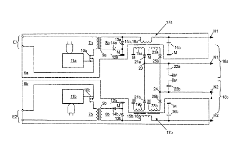
Figure 2 show a highly schematized view of the voltage
supply device 4 having the first main voltage input El
and the second main voltage input E2. Furthermore, the
two main voltage outputs H1 and H2 and the secondary
voltage outputs Ni and N2 are depicted.
Viewed structurally, the voltage supply device 4 has a
first main channel arrangement 6a and a second main
channel arrangement 6b. The first main channel
arrangement 6a is formed through the conversion of the
first input DC voltage at the first voltage input El into
the first output DC voltage at the first main voltage
output Hl. The second main channel arrangement 6b is
formed through the conversion of the second input DC
voltage at the second voltage input E2 into the second
cp.029563002()17-01-25
- 12 -
output DC voltage at the second main voltage output H2.
The first main channel arrangement 6a and the second main
channel arrangement 6b are designed identically, so that
only the first main channel arrangement 6a is described
below.
The first main channel arrangement 6a has a first input
circuit 7a and a first output circuit 8a. The first input
circuit 7a and the first output circuit 8a are coupled to
one another via a first interstage transformer 9a. In the
first input circuit 7a, a switching device 10a is in
series with a primary winding of the first interstage
transformer 9a, which, for example, is designed as a
transistor, in particular as a high-power transistor. The
switching device 10a is controlled via a control device
ha. For example, the switching device 10a is controlled
via a pulse width-modulated signal.
The first output circuit 8a has a secondary winding at
the first interstage transformer 9a. A diode arrangement
12a is provided downstream, wherein a first output of the
secondary winding of the interstage transformer 9a is
routed to ground via a first diode 13a in the forward
direction, and the second output of the secondary winding
of the interstage transformer 9a is also routed to ground
via a second diode 14a in the reverse direction. An
output inductor 15a, which is arranged downstream from
the first output of the secondary winding of the first
interstage transformer 9a, acts as a temporary energy
store.
The first output inductor 15a is connected in series with
the first main voltage output Hl. In addition, a first
capacitor device 16a is arranged for smoothing the first
output DC voltage, via which the first main voltage
output H1 is connected to ground M.
CA 02956300m7-0i-25
- 13 -
The second main channel arrangement 6b is configured
identically, the respective components, however, each
being designated by the letter "b".
The first output inductor 15a is depicted by a primary
winding 16a of a first output transformer 17a. The second
output inductor 15b is depicted by a primary winding 16b
of a second output transformer 17b.
Furthermore, the voltage supply device 4 has a first
secondary channel arrangement 18a and a second secondary
channel arrangement 18b. The first secondary voltage
output Ni is associated with the first secondary channel
arrangement 18a, and the second secondary voltage output
N2 is associated with the second secondary channel
arrangement 18b.
The first secondary channel arrangement 18a includes a
first secondary winding 19a of the first output
transformer 17a and a first secondary winding 19b of the
second output transformer 17b. The first secondary
windings 19a, b are connected to ground M on one end. The
second outputs of the first secondary windings 19a, b are
interconnected at a node 20, wherein the node 20 is in
series with the first secondary voltage output Ni. Thus,
the first secondary windings 19a, b are arranged in
parallel with one other. Upstream of the node 20, a diode
device 21a, 21b is connected in the forward direction
between the first secondary windings 19a, b and the node
20 in each case.
The secondary channel output Ni is connected via a
capacitor device 22a to ground M in order to smooth the
first secondary output DC voltage.
CA 02956300 2017-01-25
- 14 -
The second secondary channel arrangement 18b is formed
via a second secondary winding 23a of the first output
transformer 17a and via a second secondary winding 23b of
the second output transformer 17b. One output of the
second secondary windings 23a, b is connected to ground M
in each case. The other outputs are connected via a node
24 to the second secondary voltage output N2. Upstream of
the second node 24, diodes 25a, b are each connected in
the forward direction, so that only the DC voltage
component is allowed to pass through to the second
secondary voltage output N2.
The second secondary voltage output N2 is connected via a
capacitor device 22b to ground M in order to smooth the
secondary output DC voltage.
The first and second secondary windings 19a, 23a at the
first output transformer 17a are galvanically decoupled
from one another. Likewise, the first secondary winding
19b and the second secondary winding 23h at the second
output transformer 17b are galvanically decoupled from
one another. Furthermore, the first and the second
secondary windings 19a, 23a are decoupled from the
primary winding of the first output transformer 17a. In
addition, the first secondary winding 19h and the second
secondary winding 23b are galvanically decoupled from the
primary winding of the second output transformer 17b.
Via the depicted structure, the secondary voltage outputs
Ni, N2 are each supplied with electrical energy by the
two output transformers 17a, b. As a result of the
secondary windings 19a, b; 23a, b each being arranged
electrically in parallel with one other in respective
secondary channel arrangement 18a, b, one of the
secondary windings 19a, 23a or 19b, 23b may be omitted in
each case, without this resulting in a failure of the
CA 02956300 2017-01-25
- 15 -
secondary channel arrangement 18a or 18b. Thus, the
secondary channel arrangements 18a, b are designed to be
fail-safe and/or redundant.
The primary winding 16a and the secondary windings 19a,
23a are only loosely coupled to one another via the first
and second output transformers 17a, b. Similarly, in the
second output transformer 17b, the primary winding is
only loosely coupled to the first secondary winding 19b
and the second secondary winding 23b. As a result of the
loose coupling, it is achieved that a short circuit in
one of the outputs H1, H2, Ni, N2 would not result in a
serious impairment of the other channels.
This short-circuit withstand strength is furthermore
achieved via the particular winding or winding
arrangement in the output transformers 17a, b. Figure 3
shows a schematic cross section through the output
transformers 17a. The output transformer 17b is
structured identically. Figure 3 shows the primary
winding 16a on the one hand, and the secondary winding
19a is on the other hand. The primary winding 16a is
shadowed or dark; in contrast, the secondary winding 19a
is depicted as white. The output transformer 17a has a
core 26 which is designed as an E-core. The core 26
comprises a center leg 27 and two outer legs 28a, b.
Furthermore, the core 26 is covered by an I-cross member
29, wherein, however, an air gap 30 is provided between
the center leg 27 and the I-cross member 29.
The primary winding 16a is wound around the center leg
27. In this example, the secondary winding 19a is divided
into two sections, i.e., into a first secondary winding
section 31a which is also wound around the center leg 27,
and into a second secondary winding section 31b which is
CA 02956300 2017-01-25
- 16 -
wound around one of the two outer legs, in this example
28a.
This particular winding result in an inherent overload
resistance of the output transformer 17a. As a result of
the primary winding 16a being wound around the center leg
27 and the secondary winding 19a being divided into the
first secondary winding section 31a and the second
secondary winding section 31b, wherein the first
secondary winding section 31a is also wound around the
center leg 27 and the second secondary winding section
31b is wound around the outer leg 28b, it is made
possible for the magnetic flux in the core 26 to realize
a bypass path in the case of increasing loading of the
secondary winding 19a. This structure behaves like a
source impedance, which however, due to the air gap 30 in
the core 26, is primarily inductive. Thus, the short-
circuit current is limited to a maximum value. However,
since the current has a high inductive component, power
dissipation is hardly generated. The current consumption
of the associated main channel arrangement 6a is reduced
automatically during the short circuit. The other outputs
are not affected.
Thus, the voltage supply device 4 has the advantage that
the two secondary voltage outputs N1 and N2 are coupled
with the two main voltage inputs El, E2 via a particular
winding, in particular winding arrangement, and are
accordingly designed to be redundant. As a result of the
particular winding arrangement, they are also independent
of one other. Thus, a short circuit in the secondary
voltage output Ni has an effect on the other outputs. No
additional components are needed to achieve this
independence. In order to detect the failure in a diode
21a, 21b, 25a, 25b in the secondary coupling arrangements
18a, b, the main channel arrangements 6a, b, in
CA 02956300 2()17-01-25
- 17 -
particular their voltage supply, may be disconnected
individually. This approach allows testing the supply
voltage device 4 and thus the aircraft control system 1,
even during the operation of the aircraft control system
1.
CA 02956300 2017-01-25
- 18 -
List of reference numerals
1 Aircraft control system
2 Aircraft
3 On-board electrical system
4 Power supply device
5 Aircraft control device
6a, b Main channel arrangement
7a, b Input circuit
8a, b Output circuit
9a, b Interstage transformer
10a, b Switching device
ha, b Control device
12a, b Diode arrangement
13a, b First diode
14a, b Second diode
15a, b Output inductors
16a, b Capacitor device
16a, b Primary windings
17a, b Output transformers
18a, b Secondary channel arrangements
19a, b First secondary windings
20 Node
21a, b Diode device
22a, b Capacitor devices
23a, b Second secondary windings
24 Node
25a, b Diodes
26 Core
27 Center leg
28a, b Outer legs
29 I-cross member
30 Air gap
31a, b Secondary winding sections
El, E2 Voltage inputs
H1, H2 Main voltage outputs
CA 02956300 2017-01-25
- 19 -
Ni, N2 Secondary voltage outputs
V1 to V4 Power supply inputs
M Ground