Note: Descriptions are shown in the official language in which they were submitted.
CA 02956357 2017-01-25
54053PCT
DISTRIBUTED CONTROL ADAPTIVE WIRELESS POWER TRANSFER SYSTEM
CROSS-REFERENCES TO RELATED APPLICATIONS
This application claims the benefit of U.S. Provisional Application
No. 62/031131, filed July 30, 2014. This application is also a continuation-in-
part of U.S.
Patent Application No. 14/402660, filed November 20, 2014, which is a national
phase of
PCT/US2013/042085, filed May 21, 2013, which claims the benefit of U.S.
Application
No. 13/843884, filed March 15, 2013, which claims benefit of U.S. Provisional
Application No. 61/649496, filed May 21, 2012, U.S. Provisional Application
No. 61/691127, filed August 20, 2012, and U.S. Provisional Application No.
61/734236,
filed December 6, 2012.
STATEMENT OF GOVERNMENT LICENSE RIGHTS
This invention was made with government support under grant No. 1R21
HL118611-01 awarded by the National Institutes of Health, and grant No. EEC-
1028725
awarded by the National Science Foundation. The government has certain rights
in the
invention.
BACKGROUND
Wireless power transfer using inductive coupling is becoming increasingly
popular for consumer electronic devices. Commercial applications include
wireless
charging pads, electronic toothbrushes, induction cookers, and electric car
battery
chargers. However, none of these applications enable the range or geometric
freedom
that the term wireless power suggests. Charging pads and electric toothbrushes
require
that the device be placed very close to (or directly on top of) the charging
pad. This is
because the efficiency for traditional inductively coupled wireless power
transfer systems
drops off rapidly as the distance between the transmitter and receiver
increases.
Far-field wireless power transfer techniques use propagating electromagnetic
waves and are capable of delivering power to a much larger volume of space.
However,
there is an inherent tradeoff between directionality and transfer efficiency.
For example,
radio frequency (RF) broadcast methods¨which transmit power in an omni-
directional
pattern¨allow for power transfer anywhere in the coverage area. Although
mobility is
maintained, end-to-end efficiency is lost because the power density decreases
with the
square of the distance. Microwave systems with high gain antennas have been
used to
-1-
CA 02956357 2017-01-25
WO 2016/019159
PCT/US2015/042941
transfer power over several kilometers at efficiencies of over 90%. However,
these
systems suffer from the need for sophisticated tracking and alignment
equipment to
maintain a line of sight (point-to-point) connection.
Regulatory restrictions limit the amount of power that can be transmitted in
uncontrolled environments for safety, as well as emissions and interference
reasons. As a
result, the main commercial use of far-field wireless power transfer is for
passive (i.e.,
battery free) ultrahigh frequency RF identification (UHF RFID) tags, which are
limited to
four watts equivalent isotropic radiated power in the United States.
Recent research efforts using coupled resonators (MCRs) for wireless power
transfer have demonstrated the potential to deliver power with more efficiency
than far-
field broadcast approaches, and at longer ranges than traditional inductively
coupled
methods. These techniques use high quality factor ("high-Q") coupled
resonators that
transfer energy via magnetic fields that do not strongly interact with the
human body.
U.S. Patent Publication No. 2012/0153738, to Karalis et al., and U.S. Patent
Publication
No. 2012/0080957, to Cooper et al., both of which are hereby incorporated by
reference
in their entireties, disclose certain aspects of wireless energy transfer
using MCRs.
However, a drawback of current MCR systems is the inability to efficiently
adapt
to changes in the environment. For example, unpredictable loads and changes in
distance
and orientation between MCR coils rapidly change system operating points,
which
disrupt the end-to-end wireless power transfer efficiency. Dynamic adaptation
of a
system to these types of events is a critical capability in developing fully
functional and
versatile wireless power solutions.
FIGURE 1 shows a diagram of a wireless power system 90 using high-Q MCRs.
A transmitter module 91 includes a single turn drive loop 93 and a multi-turn,
spiral
resonator or transmit coil (Tx coil) 94. When an RF amplifier 92 drives
current through
the drive loop 93 at the transmitter module's 91 resonant frequency, the
resulting
oscillating magnetic field excites the Tx coil 94. The Tx coil 94 stores
energy in the same
manner as a discrete LCR tank. This results in a large oscillating magnetic
field in the
vicinity of the Tx coil 94. A high-Q coil implies that more energy can be
stored on the
coil, which also results in greater magnetic flux density at a given point in
space.
The receiver module 95 is designed similarly. It includes a multi-turn, spiral
resonator or receive coil (Rx coil) 96 and a single turn load loop 97, which
is connected
to an end device 98. The drive loop 93 and Tx coil 94 are magnetically
coupled, and the
-2-
CA 02956357 2017-01-25
WO 2016/019159
PCT/US2015/042941
load loop 97 and Rx coil 96 are magnetically coupled. Similarly, the Tx coil
94 and the
Rx coil 96 share a mutual inductance, which is a function of the geometry of
the
coils 94, 96 and the distance between them. The high-Q. Tx and Rx coils 94, 96
form a
single system of coupled resonators, which can efficiently transfer energy
therebetween.
In general (other parameters being held constant), the coupling coefficient
between the Tx coil 94 and the Rx coil 96 is inversely proportional to the
distance
between the coils 94, 96. At relatively short distances (in the over-coupled
regime), high
efficiency power transfer between the coils 94, 96 can be achieved. However,
in the
over-coupled regime there are multiple resonant modes that occur at different
frequencies. In order to achieve high efficiency in the over-coupled regime, a
wide range
of operating frequencies may be used to track the optimal frequency
corresponding to one
of these resonant modes. As the separation distance increases, the coupling
between the
resonators 94, 96 decreases, and the frequency range for high efficiency power
transfer
narrows, until the optimal frequency converges to the fundamental frequency of
the
system (critical coupling). However, as discussed below, proper tuning
techniques will
enable near constant power transfer efficiency substantially within the entire
over-
coupled regime.
In the under-coupled regime, the shared flux falls below a critical point.
Below
this point, the Tx coil 94 needs to emit more power to maintain the magnetic
field than
can be absorbed by the Rx coil 96. The result is that maximum efficiency
cannot be
achieved. Critical coupling is the point of transition between these two
regimes and
corresponds to the greatest range at which maximum efficiency can still be
achieved.
The under-coupled regime is still capable of wireless power transfer, but
efficiency
decreases rapidly as distance increases.
Therefore, for short distances between the Tx coil 94 and the Rx coil 96,
i.e., in
the over-coupled region, there can be two resonant modes at different
frequencies than
the resonant frequency of the individual coils. The low frequency mode
corresponds to
the in-phase mode and the high frequency mode corresponds to the out-of-phase
mode.
For both modes, the frequency at which the maximum power transfer efficiency
occurs
varies as the distance between the coils changes. At a sufficiently long range
between the
coils (the critically coupled region), maximum power transfer occurs at a
single
frequency: the tuned resonant frequency of the coils. Beyond this distance
(the under-
-3-
CA 02956357 2017-01-25
WO 2016/019159
PCT/US2015/042941
coupled region), the wireless power transfer efficiency drops off by one over
distance
cubed, and the maximum achievable efficiency occurs at this same frequency.
In one embodiment, the system detects these changes and performs auto-tuning
from the TX side only. This eliminates the need for an out-of-band (00B) radio
link or
backscatter techniques to transmit information from the RX side back to the TX
side. A
bidirectional coupler may be used to track the forward (al) and reflected (b
1) signals
between a power amplifier and the TX coil. By connecting the attenuated
outputs from
the directional coupler to an RF Gain and Phase Detector (GPD), the reflection
S-parameter, Si! (Si I = b 1/a 1), response can be analyzed at either a single
frequency or
for a range of frequencies. For frequency sweeps, it may be important to
ensure that the
power amplifier has a sufficiently wide bandwidth so that the output power is
consistent
at different frequencies.
In other embodiments, signals are measured at the receiver side and sent
digitally
to the transmitter using either an out-of-band radio link, or an in-band
communication
technique (e.g., backscatter or load modulation). In other embodiments, the
system
detects these changes and performs auto-tuning from the receiver side only.
SUMMARY
This summary is provided to introduce a selection of concepts in a simplified
form that are further described below in the Detailed Description. This
summary is not
intended to identify key features of the claimed subject matter, nor is it
intended to be
used as an aid in determining the scope of the claimed subject matter.
A wireless power transfer system in accordance with an embodiment of the
present invention includes a power transmitter having a transmitter controller
in signal
communication with an amplifier and a transmitter-side impedance matching
module,
wherein the transmitter-side impedance matching module is configured to
transfer power
from the amplifier to a transmit resonator. A power receiver is provided
having a
receiver controller in signal communication with a receiver-side impedance
matching
module and a rectifier that outputs a rectified voltage. The receiver-side
impedance
matching module is configured to transfer power from a receive resonator to
the rectifier.
The transmitter controller is configured to receive feedback from the power
receiver
indicating a state of the power receiver, and to use the received feedback to
adjust a
parameter of the power transmitter to produce a target rectified voltage at
the rectifier.
-4-
CA 02956357 2017-01-25
WO 2016/019159
PCT/US2015/042941
In an embodiment, the power receiver does not have a voltage regulator
component.
In an embodiment, the power transmitter and power receiver include out-of-band
radios in signal communication with their respective controllers, for
providing the
feedback from the power receiver to the power transmitter.
In an embodiment the feedback received by the transmitter is a value
indicating
the received power level.
In an embodiment the feedback received by the transmitter includes the
rectified
voltage output by the receiver rectifier.
In an embodiment the power transmitter includes a sensor that detects a
reflection
signal in the transmitter that indicates a state of the power receiver, for
example, an
S-parameter such as the voltage reflection coefficient. For example, the power
transmitter may include a direction coupler.
In an embodiment the receiver controller monitors a parameter of the power
receiver, and modulates the receiver side impedance matching module to encode
the
monitored parameter, such that the transmitter controller can decode the
encoded
parameter to receive the desired feedback, for example, the rectified voltage.
In an embodiment the power transmitter includes a sensor to detect the
presence
of a body, for example, a human, and the transmitter controller is configured
to stop or
reduce power transmission if the sensor detects the presence of a body.
In an embodiment the transmitter controller is configured to control the
transmitter-side impedance matching module to produce a target rectified
voltage from
the rectifier.
A wireless power transmitter includes a transmitter controller in signal
communication with an amplifier and an impedance matching module, wherein the
impedance matching module receives alternating current from the amplifier and
energizes
a transmit resonator for wireless transmission, wherein the transmitter is
configured to
transmit radio frequency energy to a receiver having a receive resonator
connected to a
rectifier configured to produce a rectified voltage; and further wherein the
transmitter
controller is configured to receive feedback from the receiver indicating the
rectified
voltage, and to use the received feedback to adjust a parameter of the power
transmitter to
produce a target rectified voltage at the rectifier.
-5-
CA 02956357 2017-01-25
WO 2016/019159
PCT/US2015/042941
In an embodiment the power transmitter receives feedback through an out-of-
band
radio, from a sensor that detects a reflection signal in the transmitter, or
from a modulated
signal from the receiver.
A method for wireless power transmission includes in a transmitter, generating
an
alternating current with a power amplifier and using the alternating current
to energize a
transmit resonator; in a receiver, receiving power from the transmit resonator
with a
receive resonator that is coupled to the transmit resonator and generating a
rectified
voltage for a load; providing feedback from the receiver to the transmitter
that indicates
the rectified voltage; and using the feedback to adjust the transmitter such
that the
rectified voltage is maintained at a predetermined value.
In an embodiment, a first impedance matching module is provided between the
power amplifier and the transmit resonator, and a second impedance matching
module is
provided between the rectifier and the receive resonator.
In an embodiment, the transmitter further comprises a first radio, and the
receiver
further comprises a second radio, wherein the feedback from the receiver to
the
transmitter is communicated between the first and second radios.
In an embodiment, the transmitter further comprises a directional coupler, and
the
feedback comprises a reflection signal.
DESCRIPTION OF THE DRAWINGS
The foregoing aspects and many of the attendant advantages of this invention
will
become more readily appreciated as the same become better understood by
reference to
the following detailed description, when taken in conjunction with the
accompanying
drawings, wherein:
FIGURE 1 is a diagram of a wireless power system 90 using magnetically
coupled resonators;
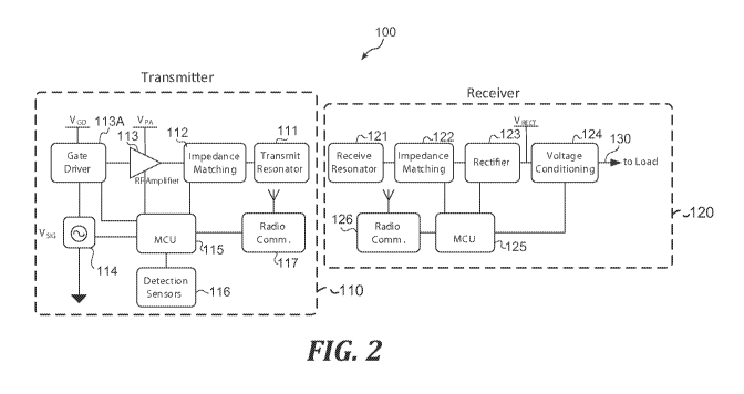
FIGURE 2 is a system level diagram of a wireless power system in accordance
with the present invention;
FIGURE 3 is a detailed depiction of a power transmitter module suitable for
use
in the system shown in FIGURE 2, that may include a directional coupler;
FIGURE 4 is a detailed schematic of a Class E power amplifier suitable for use
in
the system shown in FIGURE 2;
FIGURE 5 is a schematic of a power receiver module suitable for use in the
system shown in FIGURE 2;
-6-
CA 02956357 2017-01-25
WO 2016/019159
PCT/US2015/04294
FIGURE 6 is a schematic of a variable impedance matching module suitable for
use in the system shown in FIGURE 2;
FIGURE 7 is a schematic of a switch circuit suitable for use in the
transmitter-side
adaptive impedance matching module of the system shown in FIGURE 2;
FIGURE 8 is a schematic of a switch circuit suitable for use in the receiver-
side
adaptive impedance matching module of the system shown in FIGURE 2;
FIGURE 9 is a flow chart of a high-level operation of the system shown in
FIGURE 2; and
FIGURE 10 is a flow chart showing a power control loop that is distributed
across
the transmitter and receiver, and enables elimination of a receiver-side
voltage regulation
component.
DETAILED DESCRIPTION
A wireless power delivery system 100 in accordance with the present invention
is
shown schematically in FIGURE 2. The system 100 includes a transmitter module
110
and a receiver module 120. The receiver 120 has a rectifier 123 to convert an
RF wireless
power signal received by the receive resonator 121 into a DC voltage. In a
conventional
wireless system, the rectified voltage (VREcT) may vary over a wide range
depending on
the load power requirement and the transmit power level. If the transmitter
outputs
significantly more power than is required by the load device, VREcT will
spike,
potentially dramatically. If this happens, there are two primary concerns.
First, the
wireless power system is operating at a very low efficiency since the transmit
power level
is much greater than the load or output power. Second, the high voltage level
on the
receiver can damage the more sensitive electronics on the receiver side and
potentially
destroy the receiver circuit.
To overcome the second concern, conventional wireless power systems will
typically use an overvoltage protection circuit, or a zener diode to limit the
maximum
allowable rectified voltage. However, this does not address the problem of
inefficiency.
In order to operate efficiently, the rectified voltage should be held just
above the required
voltage for the load device or battery. However, as the distance between the
coil changes,
or the load power consumption changes, the rectified voltage will inherently
change as
well. Therefore, frequently wireless power systems also use a DC-DC converter
(or other
voltage regulation component) that converts the varying rectified voltage into
a fixed
voltage suitable for the load device, battery, battery charger (e.g., 5V, 12V,
24V, etc.),
-7-
CA 02956357 2017-01-25
WO 2016/019159
PCT/US2015/042941
etc. However for high power applications, such as charging robots or electric
vehicles on
the order of 100-1000 Watts, the DC-DC converter may be one of the most
expensive and
thermally dangerous components on the entire receiver board.
In the wireless power system 100 shown in FIGURE 2, the transmitter 110 uses
feedback from the receiver 120 to control the power that is transmitted to the
receiver 120, for example, to maintain a desired VREcr. Therefore, the system
100 does
not require a DC-DC converter. Because the transmitter 110 is actively
controlled to
achieve the desired VREcr at the receiver 120 the rectifier voltage may be
supplied
directly to the load 130, optionally with minor conditioning 124 (that does
not include
DC-DC conversion between the rectifier and the load 130).
Exemplary methods that may be used to provide feedback from the receiver 120
to the transmitter 110 include: (i) provide the transmitter 110 and the
receiver 120 with
out-of-band radio systems 117, 126, respectively, wherein the receiver 120 is
configured
to transmit relevant information from the receiver 120 (e.g., VREcT) to the
transmitter 110, for example, using WiFi, ZigBeee, or Bluetooth protocols;
(ii) provide
the transmitter 110 with a reflection sensor 116, for example, a directional
coupler that
directly detects changes in the receiver 120, e.g., through the well-known
scattering
parameters S, and in particular the input port voltage reflection coefficient
S1!; and/or
(iii) modulate an impedance matching module 122 to encode a signal, e.g., a
digital
signal, regarding the desired receiver 120 information, without significantly
interfering
with the desired power transmission from the transmitter 110 to the receiver
120.
The wireless power system 100 includes the power transmitter 110 and the power
receiver 120. The transmitter 110 includes a transmit resonator 111 that is
coupled to a
corresponding receive resonator 121 on the receiver 120 during use. A signal
generator 114, and amplifier comprising a gate driver 113A and an RF amplifier
113
drive the transmit resonator 111 through a variable impedance matching module
112.
One or more of the present inventors have disclosed suitable variable
impedance
matching modules 112 in co-pending U.S. Patent Application No. 14/402,660, the
disclosure of which is hereby incorporated by reference in its entirety.
A transmitter microcontroller 115 receives feedback from the receiver 120
from one or more detection sensors 116 (e.g., a directional coupler) and/or
with an out-of-
band radio 117, and uses the feedback to control the transmitter 110 output.
In this
exemplary embodiment the microcontroller 115 may control the power output from
the
-8-
CA 02956357 2017-01-25
WO 2016/019159
PCT/US2015/042941
resonator 111 by adjusting one, or more than one, of the signal generator
voltage, VsiG,
the gate driver voltage, VGD, the power amplifier voltage, VRA, and the
impedance
matching module 112.
The receiver 120 in this embodiment includes the receive resonator 121, that
is
operatively connected to a receiver-side variable impedance matching module
122
compatible with the transmitter variable impedance matching module 112.
Received
power is provided to a rectifier 123 to produce the desired rectified voltage.
VREc:T may
be applied directly to the load 130, or a voltage conditioning component 124
may
optionally be provided. A receiver microcontroller 125 controls the variable
impedance
matching module 122, which may be based in part on information received from
the
transmitter 110 through a compatible out-of-band radio 126. The receiver 120
also
transmits information back to the transmitter 110. Typically, the value of
VREcT is
transmitted, although it is contemplated that other related data may
additionally or
alternatively be transmitted.
The transmit resonator 111 generates magnetic fields or electromagnetic fields
from the electrical signal incoming from the variable impedance matching
module 112.
The variable impedance matching module 112 enables high power transfer
efficiency,
even as range, orientation, and/or load vary. The transmitter microcontroller
115 sets a
desired state of VsIG, VGD, VpA, and/or the impedance through the impedance
matching
module 112 to provide optimal power delivery. The signal generator 114
generates the
power transfer signal. For example, in some embodiments the power transfer
signal may
be 13.56MHz, 6.78MHz, or a lower frequency signal.
The detection sensors 116 collect information that the microcontroller 115
uses to
control various aspects of the power transfer system. In particular, the
detection
sensors 116 may include a sensor to detect reflections from the power transfer
apparatus
(e.g., resonator 111, impedance matching module 112, and/or RF amplifier 113).
A
suitable reflection signal is the voltage reflection coefficient S 11
discussed above.
The detection sensors 116 may also or alternatively include sensors to detect
proximity of a person. For example, pyroelectric motion sensors, passive
infrared
sensors, capacitive sensors, radar sensors, cameras, or other sensors may be
used for
detecting a person or object. It is contemplated that the detection sensors
may be used to
safely interrupt power transmission. For example, if a proximity sensor
detects the near-
field presence of a living body, or if an over-temperature condition is
detected, the
-9-
CA 02956357 2017-01-25
WO 2016/019159
PCT/US2015/042941
transmitter microcontroller 115 may stop power transmission from the
transmitter 110 to
the receiver 120.
Based on the data from the detection sensors 116, the microcontroller 115
adjusts
one or more transmitter 110 parameters. For example, the microcontroller 115
may
adjust the impedance matching module 112 or control the RF transmit power
level. In
another exemplary embodiment the transmitter microcontroller 115 controls the
frequency, amplitude, phase, or other properties of the signal generated by
signal
generator 114. These signal properties may be adjusted to maximize the power
transferred, or to set the power transferred to a desired level. Additionally,
or
alternatively, the signal properties may be adjusted to disable power
transfer, for
example, if no receiver is detected, or if safety sensors 116 indicate it is
presently unsafe
to transfer power, as discussed above.
The receive resonator 121 transduces the AC magnetic or electromagnetic power
transfer fields generated by the transmit resonator 111, converting the AC
magnetic fields
into AC electrical signals that are fed into receiver variable impedance
matching
module 122. The receive microcontroller 125 generates GPIO (general purpose
input/output) control signals to set the state of the variable impedance
matching
module 122 in order to optimize the power transfer efficiency, for example.
The receiver 120 may use the radio module 126 to transmit information about
power, voltage, current, efficiency, temperature or other parameters in the
receiver to the
transmitter 110, where it is received by the radio module 117.
The information that the microcontroller 115 receives from the radio module
117
is used to control one or more power transmitter 110 settings. The
microcontroller 115
may adjust transmit frequency or power settings to maximize power delivered to
the
battery and load 130, to maximize the efficiency of power transfer to the
battery and load
130, and/or to maintain a power level that is requested or required by the
receiver 120.
In some embodiments, the transmitter radio 117 and the receiver radio 126 are
configured for bidirectional communication. The high level system control
algorithm can
run entirely in the transmitter microcontroller 115, and sends commands from
the
transmitter radio module 117 to the receiver radio module 126 that are
executed by the
receiver microcontroller 125. In this embodiment, the transmitter
microcontroller 115
will also receive sensor data transmitted from the receiver radio module 126
to the
transmitter radio module 117.
-10-
CA 02956357 2017-01-25
WO 2016/019159
PCT/US2015/042941
In other embodiments, only uni-directional communication is used, e.g., from
the
power receiver 120 to the power transmitter 110. For example, sensor data may
be sent
from the power receiver radio communications module 126 to the power
transmitter radio
communications module 117, but commands will not be sent from the power
transmitter
radio module 117 to the power receiver radio module 126. In still other
embodiments,
the radio modules 117, 126 may be eliminated entirely, for example, to reduce
cost, to
improve reliability, or in applications in which the radio propagation
environment is
unfavorable, and control of the transmitter 110 components may be based on
reflected
signal detection, or information transferred by modulated power signals, as
discussed
above.
It is contemplated that the transmit resonator 111 and the receive resonator
121
may be one-coil or two-coil resonators. The system 90 shown in FIGURE 1 uses a
four-
coil resonator comprising the drive loop 93, the transmit coil 94, the receive
coil 96, and
the load loop 97. The transmit resonator 111 may include a drive loop and a
separate
transmit coil, or may comprise a single coil. Similarly, the receive resonator
121 may
include a receive coil and a separate load loop, or may comprise a single
coil. It is also
contemplated in some applications that an intermediate resonator (not shown)
may be
provided between the transmit resonator 111 and the receive resonator 121.
Refer now to FIGURE 3, showing details of an embodiment of the transmitter 110
having a low power radio module 117 with an optional directional coupler 304.
In this
embodiment, the microcontroller 115 may be, for example, a TM5320 Digital
Signal
Controller. The
microcontroller 115 controls the operations of the power
transmitter radio module 117.
The directional coupler 304 is functionally located between a power amplifier
306
and the impedance matching module 112. A relatively high power signal enters
the
directional coupler 304 from the power amplifier 306 and propagates through to
the
impedance matching module 112. The directional coupler 304 provides two low
power
outputs, a forward power output 314, and a sensed reflected (or reverse) power
output 313.
When the system is not tuned for high efficiency, relatively large reflections
will
be generated, causing a relatively large signal out of the sensed reflected
power
output 313. The ratio of the sensed reflected power output 313 to the sensed
forward
power output 314 is a measure of how well the system is tuned.
-11-
CA 02956357 2017-01-25
WO 2016/019159
PCT/US2015/042941
The fonvard power output 314 and the reverse power output 313 in this
exemplary embodiment are fed into an RF detector 305. The RF detector 305 has
two
outputs, magnitude 316 and phase 315. From forward output 314 and reverse
output 313
input signals (both AC signals), the RF detector 305 produces the magnitude
316 of the
ratio of the forward signal 314 to the reflected signals 313, as well as a
phase
difference 315 between the forward and reflected signals 314, 313. Unlike the
quickly
varying RF inputs, the output magnitude 316 and phase 315 are relatively
slowly varying
voltages. The magnitude 316 and phase 315 voltages are read by an analog to
digital
converter built in to the microcontroller 115. The combination of the
directional
coupler 304 and the RF detector 305 is one exemplary embodiment of the
detection
sensors 116.
The transmitter microcontroller 115 may control the output power level in one
or
more of several different ways. For example, the microcontroller 115 may
provide digital
commands to a digital potentiometer 308, causing a DC-DC converter 307 to
change its
output DC voltage, which is the power supply voltage for the power amplifier
306.
Alternatively, the microcontroller 115 may change the signal level using
another digital
potentiometer 312 to control the voltage generated by a DC-DC converter 311,
which is
the power supply of a gate driver 310, thus changing the input voltage to the
power
amplifier 306. The microcontroller 115 may also, or alternatively, be
configured to
change the amplitude, frequency, phase or other parameters of the original
input signal
generated by a direct digital synthesizer (DDS) 309, and provide the changed
signal to the
gate driver 310.
The various methods of adjusting the power output (e.g., adjusting the power
supply of the power amplifier 306, adjusting the power supply of the gate
driver 310,
adjusting the original input signal produced by a DDS 309) have different
advantages
depending upon the particular application. For example, one method may be more
efficient for certain signal levels, and another may provide more or less
resolution.
Persons of skill in the art will appreciate the trade-offs among the various
ways of
controlling system output power.
Refer now to FIGURE 4, showing a detailed schematic of a Class E power
amplifier suitable for use in the power transmitter 110. This Class E
amplifier circuit
takes a relatively low power input square wave and generates a high power sine
wave
output. A variable DC power supply 501 is shown, that may optionally be
implemented
-12-
CA 02956357 2017-01-25
WO 2016/019159
PCT/US2015/042941
using the DC-DC converter 307 and digital potentiometer 308 shown in FIGURE 3.
Switch 502 is a metal¨oxide¨semiconductor field-effect transistor (MOSFET)
that
accepts a control signal from a gate driver, which in one embodiment is a
square wave
alternating between OV and 7V. DC current is stored in the inductor component
503.
When the switch 502 is off (e.g., the input square wave is low), current flows
towards the
output through inductor 505. When the switch 502 is on (e.g., the input square
wave is
high), current flows through the switch 502 to ground. To ensure that minimal
power is
dissipated across the switch 502 when it is closed, inductor components 503
and
capacitor 504 are sized to ensure that the voltage during this time is zero at
the drain of
switch 502. This network is commonly referred to as a zero-voltage switching
network.
The components 503 504 also help reduce deviations from the ideal square wave,
reducing ringing and other artifacts. The inductor 505 and the capacitor 506
are a
resonant (tuned) circuit in series with the signal, tuned to the frequency of
the input
square wave. The components 505 and 506 pass the square wave's fundamental
frequency, helping convert the drain waveform into a smooth sine wave desired
for
output. Inductor 507 and capacitor 508 form a resonant circuit in a shunt or
"trap"
configuration. They are tuned to mice the target frequency. Any frequency
components
at or above twice the fundamental frequency that pass through the inductor 505
and the
capacitor 506 will be shunted to ground by components 507 and 508.
FIGURE 5 is a schematic of an exemplary power receiver 120. The rectifier 123
may be any suitable rectifier circuit as are well known in the art, including,
for example, a
simple diode bridge. In one embodiment the rectifier 123 comprises MOSFETs
driven
synchronously with the U. power signal (an alternative method of full wave
rectification). In another embodiment the rectifier 123 is a single diode for
half wave
rectification.
The receive resonator 121 may be a single loop of wire or several turns of
wire,
configured to receive magnetic flux from the transmit resonator 111. A
receiver capacitor
component 602 is selected to tune to the transmitter's fundamental frequency
for the
resonator 121 and capacitor 602.
The rectifier 123, which converts the incoming AC (or RF) signal into a DC
signal, with some ripples. Filtering capacitor 604 reduces the output ripple
by shunting
high frequency components to ground.
-13-
CA 02956357 2017-01-25
WO 2016/019159
PCT/US2015/042941
FIGURE 6 illustrates a variable impedance matching module 800 connecting a
source impedance 801 with a load impedance 802.
Matching the load
impedance 802 with the source impedance 801 maximizes the power delivered to
the
load. I-Towever, other impedance settings may be selected depending on the
application.
The impedance matching module 800 between 801 and 802 is known as a pi-match
topology. It comprises a shunt capacitor 804, 808 followed by a series
inductor 803,
followed by a shunt capacitor 806, 810.
The capacitances on the source side of the inductor 803 and the capacitances
on
the load side of the inductor 803 are broken into a plurality of sub-
capacitances arranged
in series.
The capacitor 804 is one of the sub-capacitances on the source side of the
inductor 803. The capacitor 806 is one of the sub-capacitances on the load
side of the
inductor 803. Each of the sub-capacitances is in series with an electrically
(or
mechanically) actuated switch, such as 805, 809 on the source side or 807, 811
on the
load side. When the switch 805 is closed, the corresponding capacitor 804
contributes to
the capacitance on the source side of the pi-match network 800, for example.
If the
switch 809 is closed, then the capacitor 808 adds in parallel with the
capacitor 804. By
setting the switches on the source side and the load side, the capacitances on
each two
branch of the pi-match network 800 can be varied in accordance with the
requirements of
the application.
FIGURE 7 shows a switch circuit suitable for use in the transmit side adaptive
impedance matching module 112. For example, the circuit could be used to
implement
the switch 805. This same switch design could be used for any of the transmit
side
switches: 805, 809, 807, or 811.
A control signal is applied to the gate of control MOSFET 901. When the switch
is open, the gates of MOSFET 903 and MOSFET 904 are pulled high to V DD
through
pull-up resistor 902. This design allows a lower voltage control signal (less
than VDD) to
generate a higher voltage signal better suited to actuating power MOSFETs 903
and 904.
When closed, MOSFETs 903 and 904 must provide a low impedance path between
capacitor 804 and ground. When open, MOSFETs 903 and 904 must present a high
impedance between capacitor 804 and ground. Due to their structure, power
MOSFETs
have a so-called intrinsic body diode. Because of the intrinsic body diode,
the power
MOSFET behaves not as an ideal switch, but as a switch in parallel with a
diode. The
-14-
CA 02956357 2017-01-25
WO 2016/019159
PCT/US2015/042941
orientation of the body diode is determined by the orientation of the drain
and source of
the MOSFET. The body diode allows conduction when the body diode is forward
biased,
even if the gate voltage was set in a fashion that ideally would cause the
switch to be
open (ideally would cause a high impedance between the source and drain).
MOSFETs 903 and 904 are identical but are oriented such that their body diodes
are
oriented opposite one another. This way it is never the case that both body
diodes are
forward biased. The back-to-back MOSFET configuration allows a high impedance
state
to be generated that persists throughout both the positive and negative phases
of the AC
signal that feeds through capacitor 804.
FIGURE 8 shows a switch circuit suitable for use in the receiver-side adaptive
impedance matching module 122. Because the induced AC signal on the receiver
side
fluctuates both positively and negatively with respect to the control signals,
a different,
more symmetrical design is needed on the receiver side. The MOSFET control
switch
1001 and the pull-up resistor 1002 function in the same way as the MOSFET
control
switch 901 and the pull-up resistor 902 on the transmit side. The node between
MOSFETs 1003 and 1004 is grounded. The MOSFET 1003 is connected to the
capacitor 1005, which then connects to RH- (one side of the receive coil). The
MOSFET 1004 is connected to the capacitor 1006 and then to RF- (the other side
of the
receive coil). When the MOSFETs 1003 and 1004 are both closed, the capacitors
1005
and 1006 are effectively connected in series. If the value of the capacitor
1005 is 2C and
the value of the capacitor 1006 is also 2C, then a net effective capacitance
of C is
produced when the MOSFETs 1003 and 1004 are both closed, because the
capacitors 1005 and 1006 are connected in series. When the MOSFETs 1003 and
1004
are both commanded to be open, at least one will be in a high impedance state,
because at
most one of their body diodes will be forward biased simultaneously.
FIGURE 9 is a flow chart showing an exemplary integrate control loop 200 that
would run across both the transmitter 110 and the receiver 120. In the initial
Start
state 201, the transmitter 110 is off. Data from sensors 116 or sensors in the
receiver 120
(not shown) is collected 202, to determine if a body, for example, a person,
is in close
proximity to the transmitter 110. Optionally, the sensors may also, or
alternatively,
determine if a body is in close proximity to the receiver 120. The control
loop also
monitors to determine if the receiver 120 is in reasonably close proximity to
the
transmitter 110. If no persons are detected, and the receiver 120 is near 203
then the
-15-
CA 02956357 2017-01-25
WO 2016/019159
PCT/US2015/042941
transmitter 110 is energized 204. The adaptive tuning 205 is initiated, for
example, using
power tracking, frequency tracking, or impedance matching, using feedback from
the
receiver 120 to control the transmitter 110, for example, to achieve a desired
VREcT or
other receiver parameter, as discussed above. The system tuning algorithm is
operable to
tune the system 100 for a desired operating point. During operation as the
transmitter 110
is providing power to the receiver 120, the sensors 116 continue to monitor
the operating
conditions and the transmitter microcontroller 115 adjusts one of, or more
than one of, the
power, impedance, and frequency. The system 100 monitors for the "human
absent"
condition and the "receiver present" condition 206, which both must be
positive to
continue transmitting. If a person (or animal) enters to close proximity, or
if the
receiver 120 (which may be, for example, disposed in a robot) is no longer
within
range 207, then the power transmission is turned off 208. The system may
automatically
resume transmission when a person is no longer detected, or when the receiver
120 and
transmitter 110 are back within a desired range for power transfer.
An exemplary power tracking control method 220 is illustrated in FIGURE 10,
which runs across both the transmitter 110 and the receiver 120. As discussed
above, the
transmitter 110 adjusts one or more characteristic of the transmitted power
based on a
feedback signal from the receiver 120, which allows for a simpler and/or lower
cost
receiver, for example, by eliminating the need for a DC-to-DC converter
between the
rectified power output and the load. In prior art systems, a separate receiver-
only power
control loop is generally required.
Initially, constraint values are set 221, for example, voltage target, VTAR,
and
voltage tolerance, VTOL. The receiver 120 monitors a receiver parameter 222,
typically
VREcT. The monitored parameter is feedback 223 from the receiver 120 to the
transmitter 110. As discussed above, the feedback 223 may be accomplished in
any of a
variety of ways, for example, using out-of-band radios, using detected
reflection
parameters at the transmitter 110, or by encoding the data by modulating one
of the
impedance matching or the load in the power receiver, which modulation can be
detected
by the transmitter through the coupled resonators 111, 121. The transmitter
110
interprets the feedback signals 224. In a current embodiment, if Viorr is
within VTOL
of VTAR (i.e., if VIAR-V1-01VRECT<VTAR VTOL) then no change is required, and
the
receiver 222 continues to monitor the receiver parameter 222. If VREcr is not
within
VIOL of VTAR, then the direction of the variance is determined 225, e.g., by
testing if
-16-
CA 02956357 2017-01-25
WO 2016/019159
PCT/US2015/042941
VRECT<:VTAR-VTOL. In this exemplary embodiment, if VREcr is less than A,
!TAR-VTOL,
then the transmitter 110 power is increased 226 up to a maximum setting 227,
otherwise
(i.e., if VREcr is greater than VTAR+Vroi..), then the transmitter 110 power
is
decreased 227.
While illustrative embodiments have been illustrated and described, it will be
appreciated that various changes can be made therein without departing from
the spirit
and scope of the invention.
-17-