Note: Descriptions are shown in the official language in which they were submitted.
CA 02956724 2017-01-30
1 -
PRE-PRODUCT AND METHOD FOR PRODUCING A STRIP-LIKE HIGH-TEMPERATURE
SUPERCONDUCTOR
Technical field
The invention relates to a precursor and to a method for producing a high-
temperature superconductor
(HTS) in ribbon form, and to an HTS in ribbon form obtainable by such a
method.
Prior art
High-temperature superconductors in ribbon form, also referred to as coated
conductors, comprise a
carrier substrate in ribbon form (typically consisting of metals including
precious metals, metal alloys or
metal composite materials and referred to hereinafter as "metallic"), to which
at least one superconductive
functional layer is applied, optionally after prior application of one or more
intermediate layers or buffer
layers.
An essential aspect in the production of coated conductors is the requirement
that the superconductive
layer has to have extremely high texture, i.e. crystallographic orientation.
The individual crystallites of the
superconductive layer may only be tilted slightly with respect to one another,
in order not to impair the
superconductive properties over macroscopic lengths (High Temperature
Superconductivity 1: Materials,
A.V. Narlikar (ed.) Springer-Verlag, 2004, 115-167).
In order to achieve such a high level of texture, two different production
approaches are pursued. In both
approaches, metal substrates are used, because only in this way is it possible
to achieve the strength
required for the later use and simultaneously flexibility of the end products.
Furthermore, in both
approaches, prior to the deposition of the superconductive layer, at least one
textured intermediate layer
or buffer layer is produced, which transfers its texture to the
superconductive layer on deposition thereof.
In the first approach, metal substrates that are not yet particularly suitable
in terms of their
crystallographic orientation are used as starting materials, and the buffer
layer having the desired
orientation is subsequently applied thereto. Such directed deposition can be
effected only by means of
physical coating methods, for example ion beam assisted deposition (IBAD) and
inclined substrate
deposition (ISD), under high vacuum. These processes are associated with a
high level of apparatus
complexity.
CA 02956724 2017-01-30
- 2 -
In the second approach, the metal substrate itself is textured by specific
methods (see, for example, DE
101 43 680 C1, CN 1 117 879 C, DE 100 05 861 A1). This texture of the metal
substrate is then
transferred to the buffer layer and thence to the superconductive layer in the
subsequent steps. Since no
directed deposition methods have to be used for the applying of the further
layers, it is possible here to
use either physical methods or, in particular, chemical methods such as
chemical solution deposition
(CSD).
JP 2011 113662 A discloses a "metal base material for thin film
superconducting wire, method of
manufacturing the same, and method of manufacturing thin film superconducting
wire" (title of the
abstract). According to the abstract, the metal base material has two ceramic
layers on the opposite sides
of the superconducting wire. The two ceramic layers are produced by the
heating of the metal substrates
in a film-depositing device.
DE 101 59 646 C1 discloses a "method for only single-sided coating of a planar
substrate with a layer of
high-temperature superconductor material" (title). The substrate has been
applied to just one side of the
high-temperature superconductor material. The substrate forms a planarizing
layer (paragraphs [0011] to
[0013], [0020] and fig. 1) on the reverse side of the high-temperature
superconductor material.
DE 10 2013 210 940 B3 discloses "Coating of Technical Substrates for
Manufacturing Super-Conducting
Layers with High Transition Temperature" (title). Additionally disclosed is a
method for applying a
smoothing layer to a ribbon substrate for subsequent manufacture of a high-
temperature superconductor
ribbon conductor, having the steps of: (a) applying a polysilazane-comprising
liquid to at least one side of
the ribbon substrate; and (b) heating the polysilazane-comprising liquid to a
temperature of 450 C for
deposition of a layer.
Both in terms of equipment and in terms of operating costs, chemical methods
such as the CSD method
are particularly economically viable, since they typically work at standard
pressure and enable a high
deposition rate. At the center of current development studies are therefore
production processes for
coated conductors, in which first one or more buffer layers and then the
superconductive layer are applied
to a textured metal substrate via chemical deposition. Subsequent
crystallization of every layer applied
and pyrolyzed beforehand achieves the effect that the texture of the textured
layer immediately beneath in
each case, or of the metal substrate, is transferred.
One function of the buffer layer(s) is to prevent the corrosion of the metal
substrate by oxidation, which
would result in loss of orientation at least at the metal surface; secondly,
the diffusion of metal ions such
CA 02956724 2017-01-30
- 3 -
as nickel or iron into the superconductive layer has to be prevented, in order
not to impair the quality
thereof. In the worst case, the superconductive properties of the material
would be lost.
In the final HTS crystallization annealing of an HTS precursor for
crystallization of the HTS precursor layer
applied finally (or else even in the pyrolysis of the HTS precursor layer or a
buffer layer), however, the
high temperatures that are used and the oxygenous and in some cases moist
atmosphere in the thermal
treatment can result in damage to the textured metal substrate, especially by
oxidative processes. This is
not necessarily detrimental on the front side (the first ribbon side),
provided that already adhering buffer
layer(s) (especially nonconductive buffer layers) have already been applied
thereon, and electrical
connection is additionally still possible via the backside.
Object of the invention
It is therefore an object of the invention to protect an HTS precursor,
especially the ribbon backside
(second ribbon side), from damage by oxidative processes during the HTS
crystallization annealing, or
even during the pyrolysis. At the same time, electrical coupling should
preferably not be prevented.
Subject matter of the invention
According to the invention, this object is achieved by a precursor according
to the appended claims, and
by a corresponding method and a corresponding HTS in ribbon form.
The invention relates (in general terms) to a precursor for production of a
high-temperature
superconductor (HTS) in ribbon form, comprising
a metallic substrate in ribbon form having a first ribbon side and a second
ribbon side, wherein,
on the first ribbon side,
(a) the substrate has a defined texture as template for crystallographically
aligned growth of a
buffer layer or an HIS layer
and
CA 02956724 2017-01-30
- 4 -
(b) an exposed surface of the substrate is present or one or more layers are
present that are
selected from the group consisting of: buffer precursor layer, pyrolyzed
buffer precursor layer,
buffer layer, HTS precursor layer, pyrolyzed HTS buffer precursor layer and
pyrolyzed and further
consolidated HTS buffer precursor layer,
and,
on the second ribbon side, at least one ceramic barrier layer that protects
the substrate against
oxidation or a precursor which is converted to such a layer during the HTS
crystallization annealing
or the pyrolysis is present,
wherein, when one or more layers are present on the first ribbon side, the
ceramic barrier layer or
precursor thereof has a different chemical composition and/or a different
texture than the layer
arranged on the first ribbon side and directly adjoining the substrate.
By means of the measure envisaged in accordance with the invention of applying
at least one ceramic
barrier layer or a precursor thereof on the metallic underside of the HTS
precursor prior to the application
or pyrolysis of an HTS precursor layer (or of a buffer layer arranged beneath)
or to the final thermal
treatment for HTS or buffer layer crystallization annealing, it is possible to
protect the textured metal
substrate, for example a nickel-tungsten alloy, and especially the underside
thereof, from oxidative
processes in a surprisingly simple and effective manner.
In this case, the ceramic barrier layer on the backside (= second ribbon side)
of the metal substrate of an
HTS precursor, during the pyrolysis of the HTS precursor layer (or of a buffer
layer arranged beneath) or
of the final HTS or buffer layer crystallization annealing, can serve not just
for protection of the underside
of the substrate from oxidation and hence for the retention of its mechanical
and electrical properties, but
also facilitates the establishment of the desired partial oxygen pressure in
the annealing atmosphere
because the oxygen consumption of the unprotected metal substrate, which is
otherwise residence time-
dependent, is suppressed.
It is preferable that, on the first ribbon side, an individual buffer layer is
present and the buffer layer has
been grown on by epitaxial means, or that two or more buffer layers have been
grown on by epitaxial
means.
CA 02956724 2017-01-30
- 5 -
It is envisaged in this case that the ceramic barrier layer or precursor
thereof has a different chemical
composition and/or a different texture than any individual buffer layer
arranged on the first ribbon side or
any of the two or more buffer layers adjoining the substrate.
According to the invention, the ceramic barrier layer is a layer of conductive
that delays or prevents
ingress of oxygen to the second ribbon side (the ceramic material being a
metal oxide or a mixture of
metal oxides), or a precursor which is converted to such a barrier layer
during the HTS crystallization
annealing or the pyrolysis is used.
It is envisaged in accordance with the invention that the ceramic material is
an electrically conductive
metal oxide(s) or an electrically conductive mixture of metal oxides, the
conductive metal oxide or one or
more metal oxides in the conductive mixture preferably being metal oxide(s)
doped with an extraneous
metal.
The conductive metal oxide doped with an extraneous metal is preferably
selected from doped zinc oxide
(preferably Al-doped zinc oxide), doped indium oxide (preferably Sn-doped
indium oxide, e.g. 90% In203,
10% Sn02), niobium-doped strontium titanate and doped lanthanum nickelate. The
terms "conductive"
and "conductivity" always relate in this application to electrical
conductivity.
Any conductive ceramic barrier layer on the second ribbon side need not be
removed again after the HTS
crystallization annealing prior to the attachment of the shunt, since there is
conductivity on the second
ribbon side.
The doping level of the metal oxide doped with an extraneous metal is
preferably at least 1%, based on
the total number of metal ions in the barrier layer. It is more preferable
that the doping level of the metal
oxide doped with an extraneous metal is at least 5%.
In the case of alternative use of a ceramic barrier layer composed of
nonconductive metal oxide, this layer
composed of nonconductive metal oxide is preferably easily removable after the
HTS crystallization
annealing. Details relating to this aspect are given further down, with
reference to preferred processes.
The removing of the barrier layer or the oxide layer is necessary in the case
of an insufficiently conductive
execution of this barrier layer with simultaneous use of at least one buffer
layer which is itself insufficiently
conductive on the HTS side, in order to restore electrical conductivity at
right angles to the layer structure
and hence electrical connection capacity of the HTS.
CA 02956724 2017-01-30
- 6 -
It is particularly preferable here that the thickness of the layer composed of
nonconductive metal oxide is
not more than 10% of the thickness of the substrate. The nonconductive metal
oxide is preferably
selected from the group consisting of lanthanum zirconate (e.g. La2Zr207),
yttrium oxide (e.g. Y203),
lanthanum aluminate (e.g. LaA103), strontium titanate (e.g. SrTiO3) and
calcium titanate (e.g. CaTiO3). An
important selection criterion here, in addition to gas-tightness, is scratch
resistance in order to assure
processibility in RTR ovens. The abbreviation RTR ("reel-to-reel") means here
that the processing takes
place continuously from reel to reel and not in a batchwise method.
The invention also relates to a method for producing an HTS in ribbon form,
having the following step:
- providing or producing a precursor of the invention (as described
above, preferably as
identified above as preferred, especially preferably as defined in the
claims),
wherein a pyrolyzed HTS precursor layer is present on the first ribbon side,
- crystallization annealing of the precursor.
In a method of the invention, the ceramic barrier layer is preferably applied
to the metal substrate by a
CSD (chemical solution deposition) method.
CSD methods are particularly economically viable for the reasons already
mentioned in the introductory
part of the description.
Preferably, this CSD method is selected from the group consisting of dip
coating, slot die coating and
printing with subsequent heat treatment.
CSD methods and especially slot die coating via a meniscus by felt are
preferably employed in the
application of nonconductive ceramic barrier layers.
Preference is additionally given to a method of the invention having the
following additional step:
removing the ceramic barrier layer by a preferably mechanical route. Such a
process configuration is
advantageous especially in the case of use of a barrier layer having
insufficient conductivity. Particular
preference is given to configuring the removing of the barrier layer in such a
way that the metallic
substrate in ribbon form is not heated to a temperature exceeding 100 C in the
course of removal of the
barrier layer. Moreover, dislocations in the substrate that continue as far as
the HTS side should be
avoided. In this way, the stripping of the barrier layer can be accomplished
in a particularly economically
CA 02956724 2017-01-30
- 7 -
viable manner and can additionally be controlled sufficiently precisely that
the stripping is restricted to a
minimum and the metal substrate exposed again as a result is damaged only to a
minor degree. More
particularly, damage to the HTS layer should be ruled out.
The removing of the ceramic barrier layer is preferably effected by abrasion
with a diamond suspension or
by blast cleaning.
According to the invention, it may also be the case that the removing of the
ceramic barrier layer is
effected by CMP (chemical-mechanical polishing, also referred to as chemical-
mechanical planarizing),
using A1203 in water for example.
Finally, the invention also relates to an HTS in ribbon form, obtainable by
the method of the invention.
= The ceramic barrier layer envisaged in accordance with the invention, in
contrast to the layer(s) on the
first ribbon side of the metal substrate, need not be oriented, since it does
not need to transfer any
texture. However, the barrier layer should be sufficiently impervious to
substantially protect the metal from
oxidative attack during the HTS crystallization annealing; such an attack can
alter the mechanical strength
and electrical and thermal conductivity of the metal substrate.
In a precursor of the invention, it is also possible for a plurality of
adjoining barrier layers to be provided, in
which case such a precursor is produced by, for example,
first, on the second ribbon side, applying a first barrier layer of conductive
or (alternatively)
nonconductive ceramic material (according to the appended claims) that delays
or prevents ingress
of oxygen to the first ribbon side (the ceramic material preferably being a
metal oxide or a mixture
of metal oxides), or applying a coating which is converted to such a first
barrier layer during the
HTS crystallization annealing or the pyrolysis
and then
applying a (preferably readily detachable and/or nonconductive) second barrier
layer atop this first
barrier layer. If one of the two component layers consists of material having
insufficient
conductivity, it is generally necessary to remove at least this component
layer again after the HTS
an
CA 02956724 2017-01-30
- 8 -
The ceramic barrier layer may consist of one of the materials which is used
for any buffer layer present or
the HTS layer on the surface of the metal substrate (in which case, however,
it has a different chemical
composition and/or a different texture than the layer arranged on the first
side that directly adjoins the
substrate), but also of a different material. As already mentioned, the
ceramic barrier layer is a layer of
conductive or (alternatively) nonconductive metal oxide (according to the
appended claims) that delays or
prevents ingress of oxygen to the second ribbon side, or is converted to such
a layer during the HTS
crystallization annealing. When the barrier layer consists of a sufficiently
oxygen-impervious metal, it is
preferably a baser metal than the constituents of the alloy used for the metal
substrate or readily forms a
sealing oxide skin.
The barrier layer need not necessarily have assumed its ultimate modification
or stoichiometry prior to a
customary HTS crystallization annealing of the precursor of the invention. It
may be entirely acceptable or
desirable in individual cases that a further oxidation or crystallization
proceeds during the thermal
treatment of the HTS precursor of the invention.
In the case of use of a conductive material for the barrier layer, it is
possible to draw an additional benefit
therefrom in the electrical coupling of the HTS in ribbon form to a metal
shunt to be attached later. This is
advantageous especially when at least one nonconductive oxide is used as
buffer layer between metal
substrate and HTS layer on the first ribbon side (HTS side).
A special case is that of the use of conductive oxides as barrier layer
material, for example extraneous
metal-doped metal oxides, e.g. aluminum-doped zinc oxide or tin-doped zinc
oxide, in which case a
doping level of at least 1%, more preferably at least 5%, may be provided. The
doping increases the
conductivity of the materials to, for example, le to 10-5 ohm/cm. A further
alternative would be the use of
a metal oxide layer which inherently already offers metallic conductivity, for
example a lanthanum-nickel
oxide layer.
The ceramic (oxidic) barrier layers for use in accordance with the invention
preferably have conductivities
of > 10-8 Scm-1, preferably of > le Scm-1.
As an alternative to the use of a conductive layer (as according to the
appended claims), the second
ribbon side (backside) of the metal substrate, prior to the HTS
crystallization annealing, can be provided
with any oxidic and nonconductive barrier layer. The restoration of the
electrically conductive area on the
first ribbon side of the metal substrate, which is necessary for the later
use, is then preferably effected by
a mechanical removal of the ceramic barrier layer after the HTS
crystallization annealing and oxygen
loading.
CA 02956724 2017-01-30
- 9 -
This can be achieved, for example, by drawing the coated second ribbon side of
the metal substrate over
a rotating felt impregnated with a diamond suspension. Remaining diamond
particles are subsequently
removed in a rinse cascade. The use of a diamond suspension having a defined
mean particle size of, for
example, 100 nm ensures that material is stripped only superficially.
Alternatively, the stripping of the ceramic barrier layer can be effected by
blast cleaning.
In this case, it should be carefully ensured that predominantly the barrier
layer is removed, and damage to
the metal substrate, which is regularly softer, down to deeper regions should
be avoided; this could result
in propagation of dislocations down to the opposite carrier substrate surface,
where it could lead to
delamination of the buffer architecture.
A preferred configuration for removal of the barrier layer and the restoration
of the metallic surface of the
metallic substrate in ribbon form is chemical-mechanical polishing (CMP), also
known as chemical-
mechanical planarizing.
A barrier layer in a nonconductive execution may consist, for example, of an
extremely thin (for example
20 ¨ 100 nm) lanthanum zirconate layer, which can be applied in a customary
manner by a CSD
(chemical solution deposition) method, for example dip coating or slot die
coating, to the second ribbon
side (backside) of the metallic substrate in ribbon form. In the case of use
of nonconductive buffer layers
on the first ribbon side (frontside, HTS side), it will be necessary to remove
such a nonconductive barrier
layer again after the HTS crystallization annealing, in order to restore the
conductivity on the backside of
the metal substrate.
Alternatively ¨ as already known from the prior art ¨ the finished
superconductor architecture can be
soldered at the top and bottom to metal foils of, for example, copper or
brass, which are connected at the
sides with a solder which then establishes electrical contact. In this way, it
is possible to construct shunt
layers from different metals or alloys and in any thicknesses.
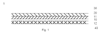
The sole figure appended, figure 1, shows a precursor of the invention by way
of example, in schematic
form and is not to scale.
The precursor 1 of the invention has a metallic substrate 10 in ribbon form
with a first ribbon side 11 and a
second ribbon side 12. The first ribbon side 11 serves to assume the layer
structure typical of an HTS, in
the present example that of a single buffer layer 20 beneath an HTS layer 30.
CA 02956724 2017-01-30
- 10 -
The backside (second ribbon side) 12 of the metallic substrate 10 bears the
ceramic barrier layer 40
envisaged in accordance with the invention for protection from oxidative
attack.
The base invention which encompasses firstly the subject matter defined in the
claims and secondly
alternative subjects is elucidated in detail hereinafter, summarizing
preferred aspects:
1.
A precursor (1) for production of a high-temperature superconductor (HTS) in
ribbon form,
comprising
a metallic substrate (10) in ribbon form having a first ribbon side (11) and a
second ribbon side
(12), wherein,
on the first ribbon side (11),
(a) the substrate (10) has a defined texture as template for
crystallographically aligned growth of a
buffer layer or an HTS layer
and
(b) an exposed surface of the substrate (10) is present or one or more layers
(20,30) are present
that are selected from the group consisting of: buffer precursor layer,
pyrolyzed buffer precursor
layer, buffer layer, HTS precursor layer, pyrolyzed HTS buffer precursor layer
and pyrolyzed and
further consolidated HTS buffer precursor layer,
and,
on the second ribbon side (12), at least one ceramic barrier layer (40) that
protects the substrate
(10) against oxidation or a precursor which is converted to such a layer
during the HTS
crystallization annealing or the pyrolysis is present,
wherein, when one or more layers (20, 30) are present on the first ribbon side
(11), the ceramic
barrier layer (40) or precursor thereof has a different chemical composition
and/or a different
texture than the layer (20) arranged on the first ribbon side (11) and
directly adjoining the substrate
(10).
CA 02956724 2017-01-30
11 -
2. The precursor according to aspect 1, wherein, on the first ribbon side
(11),
a single buffer layer (20) is present and the buffer layer (20) has been grown
on by epitaxial means
Or
two or more buffer layers that have been grown on by epitaxial means are
present.
3. The precursor according to either of the preceding aspects, wherein the
barrier layer (40) is a layer
of conductive or nonconductive ceramic material that delays or prevents
ingress of oxygen to the
second ribbon side (12), or a precursor which is converted to such a layer
during the HTS
crystallization annealing or the pyrolysis.
4. The precursor according to aspect 3, wherein the ceramic material is an
electrically conductive
metal oxide or an electrically conductive mixture of metal oxides, the
conductive metal oxide or one
or more metal oxides in the conductive mixture preferably being metal oxide(s)
doped with an
extraneous metal.
5. The precursor according to aspect 4, wherein the metal oxide doped with
extraneous metal is
selected from the group consisting of doped nickel oxide, doped indium oxide,
niobium-doped
strontium titanate and lanthanum nickelate.
6. The precursor according to aspect 4 or 5, wherein the doping level of
the metal oxide doped with
an extraneous metal is at least 1% based on the total number of metal ions in
the barrier layer.
7. The precursor according to aspect 3, wherein the thickness of the layer
of nonconductive metal
oxide is not more than 10% of the thickness of the substrate.
8. The precursor according to either of aspects 3 and 7, wherein the
nonconductive metal oxide is
selected from the group consisting of lanthanum zirconate, yttrium oxide,
lanthanum aluminate,
strontium titanate and calcium titanate.
9. A method for producing an HTS in ribbon form, having the following step:
- providing or producing a precursor (1) according to any of aspects 1 to
8,
CA 02956724 2017-01-30
- 12 -
wherein a pyrolyzed HTS precursor layer is present on the first ribbon side
(12),
- crystallization annealing of the precursor (1).
10. The method according to aspect 9, wherein the ceramic barrier layer
(40) is applied to the metallic
substrate by a CSD (chemical solution deposition) method.
11. The method according to aspect 10, wherein the CSD method is selected
from the group consisting
of dip coating, slot die coating and printing.
12. The method according to any of aspects 9 to 11, having the following
additional step:
removing the ceramic barrier layer (40) by a preferably mechanical route.
13. The method according to aspect 12, wherein the ceramic barrier layer
(40) is removed by abrasion
with a diamond suspension or by blast cleaning.
14. The method according to aspect 13, wherein the ceramic barrier layer
(40) is removed by CMP
(chemical-mechanical polishing).
15. An HTS in ribbon form, obtainable by a method according to any of
aspects 9 to 14.