Note: Descriptions are shown in the official language in which they were submitted.
CA 02956844 2017-01-30
WO 2016/023133
PCT/CA2015/050778
MULTIPLE-LASER LIGHT SOURCE
Cross-Reference to Related Applications
[0001] This application claims priority from United States Application No.
62/037543
filed 14 August 2014. For purposes of the United States, this application
claims the benefit
under 35 U.S.C. 119 of United States Application No. 62/037543 filed 14
August 2014
and entitled MULTIPLE-LASER LIGHT SOURCE, which is hereby incorporated herein
by reference for all purposes.
Field
[0002] This invention relates to light projectors. Some embodiments may be
applied to
project images for viewing. Other embodiments may be applied to create
structured light
for illumination or other purposes. Embodiments have example application in
digital
cinema, TV and home theater, portable and personal projection (military,
mobile, etc.),
indoor and outdoor personal and large screen advertising and information
dissemination,
signs/advertising/billboards/outdoor advertising, large-venue and live
performance,
medical imaging, virtual reality, computer gaming, office presentations and
collaborative
work, head-up displays in cars and other vehicles, smart illumination such as
adaptive car
head-lights, theatre spotlights, security/architectural lighting, high
contrast planetarium
projectors, indoor and outdoor general illumination systems, street-lighting,
road-lighting,
aviation lighting systems, high-contrast simulation displays such as flight
simulators, and
small-scale structured lighting for 2D and 3D printing, and laser micro-
machining.
Background
[0003] There are many situations where it is desired to create a light field
that has a
specified luminance profile. Light projection systems have a very wide range
of
applications from architectural lighting to the display of lifelike images.
The projected
light patterns can be dynamic (e.g. video), static (used for static images or
static
applications like the beams of typical car headlights projected through a lens
onto the road,
made by arbitrarily shaped optical surfaces, etc.). Light may be projected
onto a wide
1
CA 02956844 2017-01-30
WO 2016/023133
PCT/CA2015/050778
range of screens and other surfaces which may be flat or curved. Such surfaces
may be
fully reflective (like a canvas used in a cinema, a wall or a building) or
partially reflective
(such as the windshield of a vehicle). Screens may be low-gain or high-gain,
Lambertian
or highly directional, high-contrast or lower in contrast. Light may be
projected onto solid
objects or onto a medium in a volume (such as fog).
[0004] Markets for and applications of light projectors include digital
cinema, in-door and
out-door advertising, medical imaging (both for display of images, as well as
capture by a
smart light source), large venue and live events or performances, automotive
heads up
displays, car head- lights and rear-lights, automotive entertainment and
information
displays, home-theatre, portable business projection, television and displays
for consumer
applications, military applications, aviation applications (like cockpit
displays, smart
landing-assistance, individual passenger entertainment displays), structured
light sources
for industrial applications, automotive headlights and other applications.
Structured light
may also be used for high precision applications, such as curing ink or other
material for
2D or 3D printing, or steering light for laser micro-machining.
[0005] Various devices may be used to spatially modulate light. These may be
called
spatial light modulators (SLMs). Most SLMs provide a 2D array of independently
and
individually addressable pixels. Some examples of SLMs are reflective SLMs
such as
digital micro-mirror devices (DMDs), liquid crystal on silicon (LCoS) devices
and
transmissive SLMs such as LCD panels, transmissive LCD chips such as high-
temperature
polysilicon (HTPS) or low-temperature polysilicon (LTPS); and partially
reflective /
partially transmissive SLMs such as micro-electro-mechanical systems (MEMS)
based
systems in which some of incident light is transmitted and some of incident
light is
reflected. Most readily available spatial light modulation technologies are
subtractive.
These SLM technologies operate by absorbing or removing undesired light.
[0006] Other types of devices may controllably alter the nature and/or
distribution of light
using techniques that are not primarily subtractive. For example, the light
reclistributor
may exploit interference of electro-magnetic waves (light), to modulate the
distribution of
light by controlling its phase characteristics and/or modulate the frequency
of the light in
order to change the apparent colour of light. Both of these examples show how
light can
2
CA 02956844 2017-01-30
WO 2016/023133
PCT/CA2015/050778
be changed without converting energy from the light into wasted heat by
absorbing the
light.
[0007] Examples of dynamically-addressable focusing elements include:
transmissive 2D
arrays of controllable liquid crystal compartments with the property that the
compartments
can be controlled to selectively retard the phase of light, effectively
causing a change in
path-length. Devices that can controllably adjust the phase of light of
different areas are
called Phase Modulating Devices (PMD). PMDs may be transmissive or reflective.
Some
PMDs can individually control phase in a 2D array made up of a large number of
pixels. A
dynamically-addressable focusing element may also affect the polarization of
light. Some
devices may alter several light properties simultaneously.
[0008] Other types of dynamically-addressable focusing element comprise one or
more
scanning mirrors, such as a 2D or 3D microelectromechanical system (MEMS);
and/or.
one or more deformable lenses or mirrors or other optical elements. A
dynamically-
addressable focusing element may also or in the alternative comprise one or
more optical
switches.
[0009] Various sources can be used for illuminating SLMs, PMDs, imaging chips,
or any
other light re-distributing device, including arc lamps, light-emitting diodes
(LEDs), LEDs
plus phosphor, lasers, lasers plus phosphors. Each light source may emit light
of different
shapes, intensities and profiles. Traditional approaches to combining multiple
light sources
into a single higher-powered source include coupling light into optical
fibres, and knife
edge mirror beam combining, relaying into an integration rod, or some other
optical
averaging device.
[0010] However, in some cases, the useful characteristics of individual low-
powered light
sources are not preserved when combined using the traditional approaches, and
higher-
powered single-emitters are either not available, or have a prohibitively high
cost per watt
of light. For example, when light from multiple laser diodes is combined some
of the
characteristics affected are:
3
CA 02956844 2017-01-30
WO 2016/023133
PCT/CA2015/050778
= Coherence: When coupling light from multiple discrete laser diodes or
laser diode
bars into a multi-mode fibre, or combining multiple laser beams into a single
beam
using a knife edge mirror array plus lens, coherence is lost.
= Polarization: The light at the output of a multi-mode fibre is no longer
polarized, so
some polarization recovery techniques must be used for applications that
require
polarized light.
There is a need for light sources and projectors that effectively combine
light from
multiple light sources. There is a particular need for cost-effective light
sources and
projectors in which light from multiple light sources can be manipulated to
yield desired
light patterns having desired optical characteristics.
Summary
[0011] This invention has a number of aspects. One aspect provides light
sources that
combine light from a plurality of individual lower-powered light emitters
(which, in some
non-limiting embodiments comprise laser diodes or other laser light sources
and in other
embodiments comprise non-laser light sources ¨ which are solid-state light
sources in
some embodiments). The light sources may emit light in the form of arrays of
discrete,
collimated, non-overlapping patches. In some embodiments, optical paths
provided by the
light source cause the individual patches to have desired optical
characteristics such as
desired polarizations and/or coherence. Another aspect provides methods for
illuminating
a dynamically-addressable focusing element. Another aspect provides light
projectors
incorporating light sources as described herein.
[0012] Further aspects and example embodiments are illustrated in the
accompanying
drawings and/or described in the following description.
Brief Description of the Drawings
[0013] The accompanying drawings illustrate non-limiting example embodiments
of the
invention.
4
CA 02956844 2017-01-30
WO 2016/023133
PCT/CA2015/050778
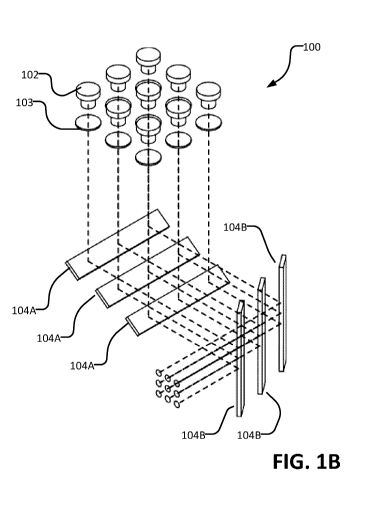
[0014] Figures lA and 1B illustrate a light source comprising a fixed diode
array with
multiple mirrors.
[0015] Figures 2A and 2B illustrate a light source comprising a fibre coupled
diode array.
[0016] Figures 3A to 3C illustrates a light source comprising a "Christmas
Tree" mirror.
[0017] Figures 3D to 3F illustrates a light source comprising a parabolic
mirror.
[0018] Figures 4A and 4B illustrate light profile resizing.
[0019] Figure 5A and 5B illustrate combining arrays of light beams from
several light
sources to yield a larger array of light beams.
[0020] Figure 6 illustrates an example optical arrangement for collimating
light beams
from light emitters having a fast and a slow axis.
[0021] Figure 7 illustrates path length equalization with multiple mirrors.
[0022] Figure 8 illustrates a DMD control scheme.
[0023] Figures 9A and 9B illustrate a possible effect of asynchronous
modulation of a
light source and operation of a DMD.
[0024] Figure 10A and 10B illustrate asynchronous modulation of a light source
and
operation of a DMD in a case where the light source is modulated at a high
frequency
relative to flip time of the DMD.
[0025] Figure 11 illustrates synchronous modulation of a light source and
operation of a
DMD.
[0026] Figure 12 is a block diagram of example apparatus for generating a DMD
sync
signal by analyzing light dumped by the DMD.
[0027] Figure 13 illustrates an example staggered start of light emitters
relative to a DMD
cycle.
CA 02956844 2017-01-30
WO 2016/023133
PCT/CA2015/050778
[0028] Figures 14A and 14B schematically illustrate different possible modes
for
controlling a dynamically-addressable focusing element to display an image.
[0029] Figure 15 is a block diagram illustrating an example projector.
[0030] Figures 16A and 16B schematically illustrate possible color imaging
modes and
ways to scale up or down optical power in a projector.
Detailed Description
[0031] Throughout the following description, specific details are set forth in
order to
provide a more thorough understanding of the invention. However, the invention
may be
practiced without these particulars. In other instances, well known elements
have not been
shown or described in detail to avoid unnecessarily obscuring the invention.
Accordingly,
the specification and drawings are to be regarded in an illustrative, rather
than a restrictive
sense.
[0032] Several novel approaches have been devised for tiling light from
multiple sources
in a parallel, collimated fashion. It is advantageous in some applications
that the tiled light
patches have minimal overlap with one another. In any of these approaches the
light
patches may be arrayed on a surface of a dynamically-addressable focusing
element such
as a phase modulator (PMD).
Adjustable Diode Array, Fixed Mirrors
[0033] A two-stage array of knife-edge mirrors can be used to tile a two
dimensional array
of lower-powered light sources, such as LEDs or laser diodes, to cover the
active area of
an imaging chip with discrete, non-overlapping patches of light. Each discrete
laser diode
(or other light emitter) is mounted in a holder with built-in X, Y and angular
adjustment,
and a lens for capturing and collimating the light. The holders each comprise
a two-axis
stage, and a holder with a tip/tilt adjustment in some embodiments.
[0034] This limits the compactness of the light source arrangement, so two
arrays of knife
edge mirrors are used, oriented 90 degrees to each other. Figures lA and 1B
show an
example light source 100 which applies this type of approach. Light source 100
includes
6
CA 02956844 2017-01-30
WO 2016/023133
PCT/CA2015/050778
light emitters 102, lenses 103, knife-edge mirrors 104A and 104B. Mirrors 104A
and
104B are arranged at 90 degrees to one another.
[0035] If space or design constraints force more complex geometry, two knife
edge arrays
can be combined in other orientations to achieve closely spaced parallel
beams.
[0036] The knife edge mirrors serve to reduce the spacing of the individual
beams, and
clip the edges to minimize overlap and maximize coverage. Each beam may
diverge
slightly, and to different degrees along the long and short axis, so the
mirror assembly is
kept compact. The distance from the output of the mirror assembly to the
imaging chip is
kept as small as is practical.
Fixed Diode Array with Adjustable Mirrors
[0037] In another example embodiment, a 2-dimensional grid of light emitters
(e.g. laser
diodes) is fit into a fixed mount machined to tight manufacturing tolerances,
with inset
collimating lenses. Light beams emitted by the array of light emitters are
directed at a two-
stage array of knife-edge mirrors. In this embodiment the light emitters
remain fixed and
alignment is achieved by moving the mirrors. Once alignment has been achieved
the
mirrors may be permanently set, such that the output of the opto-mechanical
system is a
two-dimensional array of discrete, non-overlapping patches of light. This
embodiment
may otherwise be very similar or the same as the embodiment illustrated in
Figures lA
and 1B.
[0038] This adjustment can be achieved by mounting each mirror on a pivot
joint, which
can be set with an adhesive once adjusted, or a flexible structure that can be
shimmed into
place.
[0039] In some embodiments knife edge mirrors are split into segments for each
source,
with individual tip-tilt control. This facilitates de-coupling individual
sources from a row
or column. Adjustable segments may be adjusted to apply any corrections to the
direction
or divergence of the individual beams.
[0040] Some embodiments provide adjustments to the positions and/or
orientations of
light emitters 102 as well as to the angles of mirrors 104.
7
CA 02956844 2017-01-30
WO 2016/023133
PCT/CA2015/050778
Fibre-Couple each diode
[0041] Figures 2A and 2B illustrate another embodiment wherein the outputs of
laser
diodes 102 or other light emitters are guided by optical fibers 203 to create
a desired array
of light patches. For example, the light patches may be arrayed on a surface
of a
dynamically-addressable focusing element such as a phase modulator (PMD). In
this
design an array of light emitters 102 each has an associated lens 103 that
captures the
emitted light, and couples it into a single-mode optical fiber 203. Fibers 203
are bundled,
and the output of the bundle is relayed onto the imaging chip (e.g. a PMD).
This approach
can be used to transform a source array into any shape, spacing, or
configuration. A
single-mode fibre will maintain polarization and coherence of laser light, but
this same
approach can be implemented with multi-mode optical fibers, with optimal
diameter and
geometry for increasing coupling efficiency without significant losses in
coherence or
excessive divergence.
"Christmas Tree" Mirror Mount
[0042] Instead of tiling patches in a rectangular pattern as shown , for
example, in Figures
lA and 2A, a radial pattern of light patches can be achieved by using a mirror
having a
generally conical "Christmas tree" design. One potential configuration 300 is
illustrated in
Figures 3A to 3C. In this embodiment, light emitters 102 are mounted radially
facing
inward toward a Christmas tree mirror 304. In the illustrated embodiment,
mirror 304
comprises a plurality of generally conical axially spaced-apart mirror
surfaces 304A and
304B. The approach exemplified by Figures 3A to 3C can also be expanded, by
machining
lens curvature into the mirror surfaces 304A and 304B to collimate the beams,
reduce the
spacing, and aperture the beams in a single step.
[0043] A large source spacing may be used to improve alignment at the expense
of the
overall size of the opto-mechanical system.
[0044] If consistent polarization is required, angles may be taken into
account to maintain
consistent polarity in each beam as it hits the imaging chip or other
destination.
8
CA 02956844 2017-01-30
WO 2016/023133
PCT/CA2015/050778
Parabolic mirror for combining radial beams
[0045] Figures 3D, 3E and 3F show an arrangement 300A which is similar to
arrangement
300 but uses a parabolic lens 304A to deflect beams from a radial arrangement
of light
emitters 102A, 102B into a parallel, closely spaced arrangement. In the
illustrated
embodiment, the emitters include light emitters 102A which direct beams at
mirror 304A
at a first angle to the axis of symmetry of mirror 304A and light emitters
102B which
direct light beams at mirror 304A at a second angle to the axis of symmetry of
mirror 304.
This concept is similar to the "Christmas Tree" approach illustrated in
Figures 3A to 3C,
but without the aperturing effect of mirror edges.
De-magnification of over-sized beam grid
[0046] The target illumination area, such as an imaging chip, SLM, or PMD, may
be small
compared to an array of sources. Any of the above approaches, including the
knife-edge
mirror approach described with reference to Figures lA and 1B can be used to
create a
tiled pattern of non-overlapping patches of light (i.e. an array of parallel
light beams) on a
scale that is larger than the target area. In some embodiments, the scale of
the patches of
light is a factor of 2 or more times larger than the target area (e.g. the
patches of light
cover an area 4 or more times that of the target area in some embodiments). An
optical
system can be used to reduce the area of the resulting cluster of beams by
demagnifying
the light beams such that the array of patches of light is adjusted to the
size required.
[0047] An example arrangement 400 is shown in Figures 4A and 4B. An optical
system
401 (for example any of the systems described above) creates an array of beams
402. An
optical system 404, in this example comprising lenses 404A and 404B de
magnifies the
array of beams.
[0048] Gaps may be maintained between the parallel beams, so divergence or
distortion in
the de-magnified light profile may be avoided.
Cascading knife-edge mirror stages
[0049] In some embodiments Individual modules each comprising a plurality of
light
emitters as described above can be produced in configurations which each yield
an array
9
CA 02956844 2017-01-30
WO 2016/023133
PCT/CA2015/050778
of light patches (for example a 3x3 or 3x2 configuration). Beams output by two
or more of
such modules may be de-magnified as illustrated in Figures 4A and 4B , and
tiled using an
adjustable mirror technique, as described above (e.g. using arrays of tiltable
mirrors
arranged as shown in Figure 1A).
[0050] Figure 5 illustrates an example system 500 in which light output by
three modules
401 is deflected by mirrors 502 to form an array 503 of patches of light.
Light from any
suitable number of modules 401 may be combined in this manner. Array 503 may
combine arrays from modules 401 in a linear manner, as shown, or may combine
arrays
from modules 401 to yield an output array 503 that is larger in each of two
dimensions
than the arrays of patches of light from individual modules 401. For example,
the arrays of
patches of light from modules 401 may be arranged to make a composite array
having
plural rows and columns of arrays from individual modules 401.
Light Emitters
[0051] Any of a wide variety of light emitters may be used in the embodiments
described
above, for example, the light emitters may comprise lasers. Solid state lasers
such as laser
diodes are practical for a range of applications. Other examples of light
emitters include
solid-state light emitters such as light emitting diodes (LEDs); plasma light
emitters; cold
cathode light emitters; lamps, etc. In some embodiments the light emitters
emit coherent
light. In some embodiments the light emitters emit polarized light.
[0052] Light emitters may be provided in the form of discrete devices or may
be packaged
together in packages combining plural light emitters. For example, light
emitters in
embodiments as described above may be provided using systems comprising
multiple light
emitters, such as diode bars, with appropriate emitter count and spacing. Such
embodiments may be advantageous for reducing the number of separately-mounted
components in a light source.
[0053] Some light emitters may emit light in a form which is advantageously
corrected to
yield a beam with desired properties (e.g. a beam that is well collimated and
directed in a
desired direction). Custom optics may be provided for beam conditioning and
correction
for beam path in some embodiments.
CA 02956844 2017-01-30
WO 2016/023133
PCT/CA2015/050778
[0054] Figure 6 shows an example apparatus 600 comprising an edge-emitting
diode array
602 which provides a plurality of individual light emitters 102C. Each light
emitter 102C
has a fast and slow axis. Apparatus 600 includes collimating optics 605 which
includes a
lens 605A for collimating in one axis and a plurality of lenses 605B for
collimating in a
second axis to yield a line of collimated output light beams. Two or more sets
of apparatus
600 may be stacked to provide a two dimensional array of emitters.
[0055] Especially where an off-the-shelf diode bar is used for array 602, some
conditioning and "smile correction" may be provided in the optical system in
the case that
the line of emitters has some curvature. An aperture, or reverse knife edging
may be
provided to increase the separation between beams. This can facilitate
substantial
elimination of overlap between adjacent beams.
Dealing with Path Length and Divergence
[0056] Most light emitters do not emit perfectly collimated beams of light. A
beam of
light from a light emitter will generally exhibit some divergence. It is
desirable to reduce
the effect of such divergence. In cases where divergence of the beams from
different
emitters can be substantially eliminated, an output array of patches of light
may have the
patches spaced very close to one another without any significant overlap
between the
patches. Some light emitters emit light that diverges differently in different
directions. A
direction in which the divergence is large may be called the fast axis. A
direction in which
divergence is smaller may be called a slow axis. Where a light emitter has a
fast and a
slow axis, a single symmetrical lens can approximately collimate a beam from
the light
emitter along the fast or slow axis, but the beam will continue to diverge in
the other axis.
Pairs of mirrors to fix path length
[0057] Some embodiments equalize path length from the light emitters to the
corresponding patches at the target area. Making path lengths equal for all
beams is
advantageous at least in part because beam divergence can differ for different
path lengths.
Where the path lengths are equal, divergence of all of the beams may be
approximately
equal.
11
CA 02956844 2017-01-30
WO 2016/023133
PCT/CA2015/050778
[0058] Mirrors can be used to fold the light path to equalize the path length
across all
beams, as shown in apparatus 700 of Figure 7. Using multiple mirror stages,
the path
length for each beam can be identical without complex geometry. Apparatus 7
includes
light emitters 102 that emit light beams 103-1, 103-2 and 103-3. Each beam
interacts with
a pair of mirrors that fold its path. the mirrors are spaced so that the path
lengths from each
light emitter 102 to output beams 703 are equal. Apparatus 700 includes mirror
pair 701A-
1 and 701B-1 which acts on beam 103-1; mirror pair 701A-2 and 701B-2 which
acts on
beam 103-2; and mirror pair 701A-3 and 701B-3 which acts on beam 103-3.
Asymmetrical Lenses
[0059] Light profiles of source light beams may not be radially symmetrical,
either in
terms of shape, or rate of divergence. For example, the fast and slow axis of
a laser diode
have different rates of divergence. This can be corrected by introducing a
lens that is not
circularly symmetrical in the beam direction (e.g. a cylindrical lens) in the
light path.
[0060] Some embodiments provide an array of cylindrical lenses to correct the
divergence
along the slow axis of beams from a plurality of light emitters such as laser
diodes. This
approach is well-suited for the case where diode bars or a diode bar stack
provide the light
emitters. This approach may also be applied to an array of discrete diodes or
other light
emitters. An example is illustrated in Figure 6.
[0061] Various possible optical arrangements to correct divergence of beams
having a fast
and a slow axis include using pairs of cylindrical lenses for each axis, using
a single
shared spherical lens and a cylindrical lens for each axis and so on.
Long Geometry
[0062] As described above, the effects of divergence can be mitigated by
designing the
source array such that distance from the source array to the mirrors which
guide the light
into parallel beams (e.g. knife edge mirrors as shown in Figure 1A) is large,
relative to the
distance between the knife-edge mirrors and the target area (e.g. a
dynamically
addressable focusing element or other imaging chip). In some embodiments the
distance
12
CA 02956844 2017-01-30
WO 2016/023133
PCT/CA2015/050778
from the light emitters to the mirrors is at least 3, 5, 10 or 18 times larger
than the distance
from the mirrors to the imaging chip.
[0063] With this approach, increasing the distance from the light emitters to
the mirrors
makes any relative differences in path lengths for different beams smaller.
The mirrors
may be close enough to the imaging chip that the amount of divergence between
the
mirrors and the imaging chip is small, such that no undesirable overlap occurs
at the
imaging chip.
Desired Light Source Characteristics for Freespace laser projector using phase
and
amplitude modulation
[0064] In a traditional digital projector, it is important that the amplitude
SLM (DLP,
LCD, LCoS) which is imaged onto the projection screen via the projection lens
is
illuminated uniformly.
[0065] In some embodiments a light source illuminates a dynamically-
addressable
focusing element non-uniformly. In such embodiments dynamically-addressable
focusing
element (e.g. a phase modulator) may be controlled to provide structured
illumination
(which varies from location to location in a known way) on an amplitude SLM.
While it
remains beneficial to illuminate the phase modulator uniformly (even heat
dissipation,
uniform light profile on SLM when a flat phase is addressed or in case the
phase SLM
fails), intensity variation across the phase SLM can be accounted for and the
lensing
pattern can be adjusted to 'correct' for it (for example to provide uniform
illumination on
the amplitude SLM when desired).
Alignment Example
[0066] A light source for a particular application desirably achieves
specifications
required by the application for beam quality and stability in a package that
is simple and
compact. Ideally the light source may be installed as a single module which
can be aligned
at time of manufacture using adjustments that facilitate rapid accurate
alignment (e.g.
orthogonal adjustments such that adjustment of one beam property does not
change other
beam properties).
13
CA 02956844 2017-01-30
WO 2016/023133
PCT/CA2015/050778
[0067] In some embodiments alignment is performed in a 'bottom-up' approach in
which
light beams from individual light emitters are centered and collimated, the
light emitters
are assembled into banks, the alignment of the beams is adjusted, and then
beam shrinking
optics are adjusted to deliver the output light to a desired target area (in
some
embodiments the target area is a few mm per side, for example 12x7mm). After
each
alignment step the adjustment may be fixed using a settable material such as a
suitable
epoxy, glue, solder or the like.
[0068] Table I provides three sets of example design specifications. Some of
these
specifications are achieved in some embodiments. One or more of these sets of
specifications are achieved in some embodiments.
TABLE I ¨ Example Design Specifications
Priority Feature Good Better Best Unit Comments / Metrics
specs specs specs
1 Z-Parallelism 500 210 0.5 arc sec Fast axis,
measure on
optical axis at .1m, .5m
and 5m distance
6.4um resolution,
300mm away
2 XY Parallelism 15 2 0.5 Degrees
(in-plane tilt)
3 XY-Shifting 50 10 0.1 px
(tiling) (LETO)
4 Divergence mrad
(fast axis)
Divergence mrad
(slow axis)
Fill-factor on 40 95 99 % LETO Fill factor is a
function
LETO area of beam size and
diode count. Need to
modify one or the
other
6 Intensity 40 75 95 0/0
uniformity on relative
LETO to peak
7 Measurement absent Present, absent
port removable
14
CA 02956844 2017-01-30
WO 2016/023133
PCT/CA2015/050778
TABLE I ¨ Example Design Specifications
8 Beam stability unknown quantified constrained %
Meet 1,2,3 after lh,
over time variation 6h, 24h
9 Beam stability unknown quantified constrained %
Meet 1,2,3 at 20C,
over variation 40C, 60C
temperature
Beam stability unknown quantified constrained % (Profile,
Centre
over power variation Location,
Intensity)
Consistency &
predictability over
various modulation
approaches, PWM,
current control, etc.
11 Throughput 60 75 90 0/0
Example Light Source Block
[0069] In this example, eight laser diodes, each with a corresponding
collimating lens, are
positioned in an array, with lOmm separation distance. Each diode is pressed
into a copper
block with integrated cooling fins, and attachment features. Eight lenses are
mounted in a
fixed block with lOmm spacing. A jig holds the fixed lens array stationary
relative to an
alignment pattern some arbitrarily large distance away, in the far field. This
alignment
pattern includes reference lines indicating desired beam positions, with lOmm
spacing.
[0070] A single diode block is held in a three-, four-, five-, or six-axis
positioning stage,
and positioned such that the emitter is centered with respect to the
corresponding lens, the
output beam is collimated (neither diverging or converging in the far-field),
oriented so
that the polarization is consistent with the light source specification, and
directed such that
the beam is coincident with the corresponding position indicated on the
alignment pattern.
[0071] The z-axis position of the diode emitter (parallel to the beam
direction) controls the
divergence of the beam. The x- and y- axis position of the diode emitter
control the x- and
y- location of the laser spot on the alignment pattern. Rotation about the z-
axis controls the
polarization orientation. The x- and y- axis position of the diode emitter can
be adjusted to
correct for distortions in the beam shape.
CA 02956844 2017-01-30
WO 2016/023133
PCT/CA2015/050778
[0072] When the diode is suitably positioned, it is fixed to the lens block.
This mechanical
connection can be achieved in a number of ways such as::
1. The diode block has tabs that are soldered to pads on the lens block
2. The diode block remains in the jig, and an adhesive such as epoxy or a
suitable
UV-curing adhesive or a suitable thermal curing adhesive is applied to fix the
diode position,
3. The diode block is spot welded to lens block,
4. The diode block is initially aligned coarsely and is precisely deformed in
the jig for
fine alignment.
Techniques for Improving Alignment Precision
[0073] With a printed alignment mask on the example system described,
collimation and
parallelism accuracy is limited to on the order of +/-lmm at a distance of 3m,
or 0.015
degrees.
[0074] For improved accuracy, more advanced techniques can be implemented.
Some
examples are:
1. A diffraction grating can be positioned in the light path, to produce
larger
alignment patterns with diffractive imaging, and magnified for increased
measurement accuracy.
= The collimation can be adjusted to achieve the optimal point spread
function to
a much higher precision.
= The parallel beam alignment precision can be improved by registering two
alignment patterns rather than attempting to centre an amorphous beam dot on
an alignment grid visually.
2. A dynamic diffractive optical element, such as a phase-only Spatial Light
Modulator, can also be used to improve alignment precision, by dynamically
changing the diffractive alignment pattern for a multi-step alignment
approach.
= Sets of alignment patterns can be generated, starting with coarse
patterns, and
moving to progressively finer alignment.
= Different patterns may be better suited to achieving different aspects of
alignment. For example, horizontal lines for XZ-plane alignment, vertical
lines
16
CA 02956844 2017-01-30
WO 2016/023133
PCT/CA2015/050778
for YZ-plane alignment, a suitable horizontally and vertically symmetrical
pattern for collimation adjustment, or for optimizing the beam angle about the
optical axis etc.
Automation of Light Source Alignment
[0075] The alignment process can be automated, diode-by-diode, using computer-
controlled 4-, 5-, or 6-axis alignment stages, and either a machine vision
camera directed
at a screen, or by relaying the output beams onto an optical sensor, such as a
CCD, or
CMOS. The following is an example algorithm that may be applied for automated
or semi-
automated alignment. The algorithm begins with a fixed block of lenses,
mounted to an
alignment jig. For the duration of the alignment procedure, the lens array may
remain
fixed relative to the all other elements, excluding the diodes. The alignment
jig holds the
lens array block, pointed at a dynamic diffractive optical element (e.g. a
phase modulator).
Light output from the phase modulator is resized using standard optics, and
relayed onto
an optical sensor, or projected onto a screen and captured by a machine vision
camera. The
diffractive optical element and screen or optical sensor are placed at a
distance that is very
large compared to the focal length of the lenses in the fixed array.
1. Begin
2. Position the light emitter (e.g. a laser diode) in approximate alignment
with the
corresponding lens and clamp the laser emitter in a jig, providing 4-, 5-, or
6-axis
micro-positioning. The jig may comprise a stage, and a holding device.
3. Proceed with the automated alignment procedure:
a. Apply a flat phase pattern to the dynamic diffractive optical element, and
adjust the focus by moving the light emitter so that the beam neither
converges nor diverges. This can be achieved by sampling the beam profile
at several distances along the optical axis and adjusting the distance
between the laser diode and the lens until all samples are the same width.
This can also be achieved using a beam splitter and a phase sensor, and
adjusting the position of the laser emitter until the beam profile is
maximally flat.
b. Insert a polarizer into the light path (if the dynamic diffractive optical
element is not polarized, or if it is not polarized in the desired direction).
17
CA 02956844 2017-01-30
WO 2016/023133
PCT/CA2015/050778
Adjust the angle of the light emitter about the optical axis, holding all
other
adjustments constant, until the beam reaches maximum brightness.
c. Apply alignment patterns to the dynamic diffractive element and adjust the
position of the light emitter position until the patterns are registered
optimally. This process can be repeated for various aspects of alignment,
including XZ-plane parallelism, YZ-plane parallelism, rotations about the
X or Y axes.
d. This alignment procedure can be repeated in multiple steps, from coarse to
fine alignment
4. When sufficiently precise alignment is achieved for the light emitter-lens
pair, fix
the light emitter to the lens block using one of the methods described above.
5. Repeat the above steps for each additional light emitter adjusting for beam
characteristics as above and also ensuring that the beam is parallel to the
beams of
previously-aligned light emitters added to the block.
Combined System
[0076] Once a block of light-emitter-lens pairs has been aligned to yield
collimated,
parallel beams, with identical polarization orientation the block may be
combined with
other elements which function to create a more compact beam array, and to
shape and
resize the combined light profile to cover an imaging chip. Such a system
might comprise:
= a mount to hold the array of diode-lens pairs;
= an array of knife-edged mirrors arranged to decrease the spacing between
adjacent
beams;
= one or more lenses or mirrors for expanding or contracting the beam to
suit the
desired application;
= mirrors for folding the light path to achieve a compact footprint and/or
to equalize
path lengths or different beams;
= cooling for the heat-generating elements (e.g. suitable heat sinks and/or
active
coolers such as Peltier elements); and
= control electronics for the light emitters.
18
CA 02956844 2017-01-30
WO 2016/023133
PCT/CA2015/050778
[0077] Some embodiments also include monitoring sensors such as temperature
sensors
attached to measure operating temperatures of the light emitters and/or other
elements and
/or measurement ports at which beam profiles may be evaluated.
[0078] In an example embodiment the light emitters comprise 500 mW lase diodes
such as
the model ML501P73 laser diodes available from Mitsubishi electric, these
laser diodes
output light at 638nm. An example display includes 6 to 20 such laser diodes.
Control Electronics
[0079] It is not always desired to have light emitters running at full
brightness at all times
due to the fact that some images do not contain much light. It is possible to
steer unneeded
light into a dump area (e.g. through suitable control of a dynamically-
addressable focusing
element), but it would be more ideal to reduce the light output of the light
emitters and
reduce energy consumption and heat output. Reducing the output of the light
emitters for
darker images may also improve black level by reducing scattered light.
[0080] Laser diodes can be dimmed by reducing the amount of current passing
through
them and or turning them off and on at a sufficiently rapid speed to not be
noticeable by a
human observer ¨ known as pulse width modulation (PWM). It is more difficult
to achieve
precise intensity control by controlling the current than by PWM.
[0081] When using PWM control a duty cycle (% of the time that a light emitter
is ON)
can be thought of as controlling the output light intensity. For example one
way to
implement 8 bit control over light intensity is to clock a counter at 256x the
PWM
frequency such that an output is held in a state corresponding to the light
emitter being ON
until the counter value reaches the 8 bit intensity value. The output would be
in a state
corresponding to the light emitter being OFF at other times during each PWM
cycle..
[0082] In some projectors Digital Light Processing (DLP) devices are used to
create the
final image. It is desirable to provide a light source as described herein
which is
compatible with downstream DLP devices. In a DLP device a binary modulator
flips a
micro mirror back and forth between an "on" state where it sends light to the
screen and an
"off' state where it sends light to a "dump" area. Each pixel has a
corresponding micro
19
CA 02956844 2017-01-30
WO 2016/023133
PCT/CA2015/050778
mirror. The DLP creates greyscale by flipping the micro-mirror back and forth
rapidly.
The micro mirror is controlled to spend more time in the "on" state to make a
brighter
pixel or more time in the "off' state to make the pixel dimmer.
[0083] In an example DLP driving scheme, each pixel has an 8 bit (or more)
greyscale
drive value per frame of video (usually 60 fps), these are translated into 8
mirror flip
periods, with one period for each bit. The period corresponding to the least
significant bit
is short. The period doubles for each bit and is longest for the most
significant bit.
[0084] Whether a bit is set to 0 or a 1 determines whether the mirror is
flipped to the "on"
or the "off' position for the corresponding period. Figure 8 shows that the
shortest period
that the mirror may be in the "on" or "off" state is for the lowest-order bit
(b0). This
shortest period may be called the "flip period".
Asynchronous Light Pulses
[0085] If a pulsed light source is used (for example to produce light at 50%
of the
maximum level), flickering will occur if the "off' and "on" pulses of the
light emitter are
asynchronous to the mirror flipping and the periods of "off' and "on"
significantly differ
from frame to frame on a static image due to a low pulse frequency for the
light state.
Slow Asynchronous Light Pulses
[0086] This is illustrated in Figures 9A and 9B. In frame 1 of Figure 9A the
viewer
perceives two light pulses during the time the DMD transmits light. In frame 2
of Figure
9B the viewer perceives three light pulses during the same DMD open period.
This 50%
change in light intensity is due to the light pulses being asynchronous to the
mirror flips.
Fast Asynchronous Light Pulses
[0087] If the "off' and "on" light source periods are short relative to the
"mirror flip"
period, the difference between "off' and "on" periods between static frames
should be
drastically reduced and be imperceptible to the human eye. For example,
Figures 10A and
10B show an example in which the light emitter is modulated significantly
faster than the
DLP flip period.
CA 02956844 2017-01-30
WO 2016/023133
PCT/CA2015/050778
[0088] In Figures 10A and 10B only a single minimum width mirror flip is shown
depicting a drive value of 1. The viewer perceives a light intensity
corresponding to 27/54
in Figure 10A and to 28/54 in Figure 10B. A disadvantage of this solution is
that a large
amount of electromagnetic interference (EMI) can be produced by switching
powerful
lasers off and on very quickly. Also, tighter timing tolerances are required
by the circuitry
to minimize duty cycle distortion between lasers.
Synchronous Light Pulses
[0089] If the light emitter "off' and "on" periods are synchronous to mirror
flips, there
should be practically no difference between static frames and the light source
pulse
generator need only run at the period of the mirror flips, drastically
reducing generated
EMI and allowing for slacker timing considerations. Figure 11 illustrates an
example
embodiment in which light output from a light emitter is synchronized to DLP
flip cycles.
[0090] When a new frame arrives, the mirror flip logic for all pixels can be
updated
simultaneously via a double buffering scheme (or in blocks from top to bottom
if desired).
Synchronizing the Light Source to the DLP
[0091] Some DLP driver chips provide a "trigger out" pin that indicates the
start of a
mirror flip cycle. In absence of this an independent "mirror timing recovery"
circuit can be
constructed. When the mirror is in the "off' state it sends light to a "dump"
area. Placing a
photoreceptor in the dump area will send a voltage back to the circuit when a
mirror flips
to the "off' state. During a "training mode" the lasers are constantly on and
the DLP sends
only the least significant bit to the dump area (i.e. drive level 254 for a
DLP with 8 bit
control). Using a high speed reference clock and counters the period of the
shortest mirror
flip can be determined and the timing of subsequent mirror flips can be
predicted. Similar
methods are employed in telecom applications for clock and data recovery from
a single
wire serial data stream. A jitter attenuator may be provided depending on the
amount of
error in the recovery system.
[0092] With the recovered mirror flip period, the light source can synchronize
PWM for
the light emitters to the mirror flip periods such that a deterministic light
intensity can be
21
CA 02956844 2017-01-30
WO 2016/023133
PCT/CA2015/050778
produced for the shortest mirror flip period (and all longer periods). During
longer mirror
flip periods the PWM cycle could simply repeat (twice for bit 1, four times
for bit 2, 8
times for bit 3 etc.), or to further reduce EMI the PWM cycle period could
lengthen for
each bit.
[0093] Figure 12 illustrates an example system 1200 in which a light source
102
illuminates a PMD 1204 by way of an optical system (which may, for example, be
as
described in any embodiment discussed herein), Light 1205 is steered by PMD
1204 to
illuminate an active area of a DMD (or DLP) 1206. Pixels of DMD 1206 are
operable to
direct light to a screen 1208 or a light dump 1210. A photo receptor 1212
measures the
light incident at light dump 1210. Since this light is turned on and off at
the times that
micromirrors of the DMD 1206 flip, the output signal of photoreceptor 1212 is
modulated.
The output signal of photoreceptor 1212 is provided to a timing recovery
circuit 1214
which also receives a reference clock signal 1214A. Timing recovery circuit
determines
the timing of the DMD mirror flip cycle through analysis of the signal from
photoreceptor
1212 and generates a sync signal 1215 which is provided to PWM generator 1218.
PWM
generator 1218 receives light emitter drive values 1219 and generates PWM
signals to
cause light emitter driver 1220 to drive light sources 102 at appropriate
levels. PWM
generator 1218 synchronizes the PWM signals to sync signal 1215.
[0094] A further enhancement that may be added to reduce the maximum current
draw
from the laser power supply and somewhat reduce EMI is to shorten the PWM
period
slightly and stagger the turn on times for different light emitters.
[0095] Staggering the laser turn on times requires less maximum current
capacity from the
laser power supply because only one laser turns on at any given time. This
should also
reduce EMI produced by the power supply. Figure 13 illustrates staggered laser
turn on
times synchronized to a DMD mirror flip.
Light Emitter Temperature Control
[0096] The temperature of a laser diode affects the wavelength produced and
the
efficiency (lumens per watt). If laser output is attenuated to a low level for
an extended
period the laser may cool excessively and lumens output may deteriorate.
Worse, the light
22
CA 02956844 2017-01-30
WO 2016/023133
PCT/CA2015/050778
output may become non-deterministic relative to the PWM drive level. To
correct for this
condition, the light source may be configured to drive the lasers harder when
they are cool
and to steer the excess light to a dump area to warm the lasers up.
Alternatively, a Peltier
element (and or another heater) can be used to warm or cool a laser that is
operating
outside of a desired temperature range. An optical feedback path can be
implemented to
detect light intensity in part of the beam to measure accuracy of lumens
output in relation
to laser drive levels and temperature.
Example Applications
[0097] Embodiments of this invention can be used to provide illumination for
any of the
applications or markets described above. A light profile made up of tiled,
substantially
non-overlapping patches of coherent, polarized laser light has multiple
potential
applications. An example application is providing illumination for creating a
light field
using a phase modulating device (PMD). Outputs of the lasers may be
individually
modulated if desired. In some embodiments, polarizations of the light patches
is oriented
to match a polarization preferentially passed by the PMD.
[0098] Example phase modulation devices include:
= Spatial light modulators (SLM), for example a 1D or 2D array of pixels,
in which
the drive level addressed at a pixel correlates to the phase delay applied to
the light
impinging on that pixel, for example the drive levels between 0 and 65535 may
correspond to the range of phase delay between 0 and 27( radians (one cycle of
the
wavelength of the light).
= Such a spatial modulator can simultaneously change the state of
polarization of the
light (an example is a transmissive liquid-crystal display, or a reflective
liquid
crystal-on- Silicon display (LCoS)). Alternatively, such an SLM can be
designed to
affect the phase delay of that pixel, but not its polarization.
= An acousto-optical modulator (AOM; also called a Bragg cell) can affect
deflection angle of the incoming light, its phase, frequency and polarization
characteristics.
23
CA 02956844 2017-01-30
WO 2016/023133
PCT/CA2015/050778
= A grating light valve (GLV); currently, these devices are 1D addressable
arrays
where each pixel or element can vary the phase of the impinging light by
mechanically varying the path length.
= Deformable Mirrors; using either continuously deformable mirror surface
with an
array of control points, or arrays of discrete, individually modulated
reflective
pixels.
[0099] A phase modulation device can be used to create a desired light field.
A lens in the
classical sense is a variable thickness piece of transparent material such as
glass that
retards the phase of the incident light differently across the lens surface,
resulting in a
focused or de-focused spot of light depending on the curvature or shape of the
lens. A
similar effect can be achieved by retarding the phase of the incoming light
beam using a
phase modulating device (PMD). For example, the effect of a lens can be
achieved by
addressing a varying phase pattern on the PMD, with for example 27( phase
retardation in
the centre of the PMD, falling off to 0 phase retardation on the edges of the
PMD.
Stronger lenses (lenses with a shorter focal distance) can be achieved by
controlling the
PMD to provide phase modulation in a pattern like that of a Fresnel-lens (i.e.
by phase
wrapping the values applied to drive the PMD pixels).
[0100] A PMD may be controlled to simulate the effects of other optical
elements, such as
prisms and gratings in a similar fashion, for example by applying a slowly
varying amount
of phase delay in one direction on the PMD.
[0101] Different effects may be combined on the PMD. An example is a phase-
pattern
that both focuses and shifts the incoming light profile. This may be achieved
by
controlling the PMD to alter the phases of light in a pattern that
superimposes (adds) the
respective phase delay patterns for a lens and a prism.
[0102] Several lenses side-by-side or super-imposed on the PMD can coarsely
approximate an image. By suitably controlling a PMD to emulate the action of a
number
of lenses one can create a situation where an image or parts of an image are
in focus
anywhere along the direction of light propagation, for example in several
planes.
24
CA 02956844 2017-01-30
WO 2016/023133
PCT/CA2015/050778
[0103] A PMD may be controlled to create any of an exceedingly broad range of
output
light fields. Determining what data to use to drive the PMD to yield a
specific desired
output light field may be done in a number of ways. In a more-computationally
expensive
but more exact mode one can apply a mathematical model of the inverse
transformation
provided by the entire optical system (including the PMD) to start with the
desired output
light field and calculate the PMD pixel settings corresponding to the desired
output light
field. A less-computationally intensive but less exact mode includes setting
parameters for
one or more discrete optical elements (lenses, prisms, etc.) that can be
emulated by the
PMD to yield an output light pattern that approximates the target light
pattern. The
parameters may, for example, include sizes, locations and optical strength.
[0104] Various approaches to controlling a PMD to cause a desired image or
other light
pattern to be displayed are described in PCTCA2014051013 published as
W02015054797; PCTCA2015000324; PCTCA2015050515; and PCTCA2015050730; the
disclosures of all of which are hereby incorporated herein by reference for
all purposes.
Hybrid GS-based Imaging:
[0105] In an example embodiment, an adaptation of the Gerchberg¨Saxton
algorithm is
used to generate a pattern on a PMD to produce an image in the far field. The
Gerchberg¨
Saxton algorithm is an iterative approach to retrieving the phase of a pair of
light fields.
Given some target illumination profile, and a well-characterized input light
profile, an
iterative approach can be used to converge on a phase pattern that, when
applied to the
PMD, will approximate the target profile in the far field.
[0106] An array of parallel beams is relayed onto an active area of the PMD,
each
covering a segment of the active area, and supplying light to form a sub-image
in the far-
field. This is illustrated in Figure 14A. Misalignment caused by imperfect
parallelism of
the light beams may be corrected by superimposing a prism on the modulation
pattern
applied to a corresponding area of the PMD to shift a sub-image corresponding
to that area
into alignment so that each sub-image is overlaid correctly at the image
location.
CA 02956844 2017-01-30
WO 2016/023133
PCT/CA2015/050778
Segmented Approach
In this approach, a phase pattern is calculated for the PMD with the image
divided up into
segments, corresponding to incoming beams. This pattern can be calculated
using a similar
approach to the one described above. In this approach, light field re-
distribution using a
PMD is restricted to local redistribution within the image segment, such that
light from a
single beam is only re-directed within the corresponding image segment, as
illustrated in
Figure 14B. As described above, a prism may be superimposed on the phase
pattern in
each image segment as required, for fine alignment adjustment.
Lensing
[0107] A PMD may be controlled to simulate the effects of other optical
elements, such as
prisms and gratings in a similar fashion, for example a prism may be provided
by applying
a slowly varying amount of phase delay in one direction on the PMD.
[0108] Different effects may be combined on the PMD. An example is a phase-
pattern
that both focuses and shifts the incoming light profile. This may be achieved
by
controlling the PMD to alter the phases of light in a pattern that
superimposes (adds) the
respective phase delay patterns for a lens and a prism.
[0109] This approach can be used to in conjunction with an input light field
made up of
tiled, non-overlapping patches of light, to shift and scale individual light
patches, or small
sections of patches to approximate an image.
Free-form Lensing
[0110] Several lenses side-by-side or super-imposed on the PMD can coarsely
approximate an image. More complex images or illumination profiles can be
achieved by
controlling the PMD to present a phase adjustment that is continuously-varying
over the
area of the PMD. Such a phase-pattern can be achieved by an iterative
optimization
approach, where the difference between the current solution and the target-
image is
iteratively minimized until a completion criterion is satisfied.
[0111] The optimizer finds a solution using a minimization or optimization
approach
based on a forward model and its inverse. An initial guess of the light re-
distribution
26
CA 02956844 2017-01-30
WO 2016/023133
PCT/CA2015/050778
scheme as well as regularization terms may be utilized to converge towards a
suitable
solution in fewer iterations. System constraints may also be supplied. An exit
metric, for
example the maximum number of iterations, a residual, or a perceptual metric,
determines
when the program stops and outputs the current solution in form of a light re-
distribution
scheme.
[0112] An optimization approach can be applied where the incoming light is in
the form
of a 2D array of parallel beams. The input light distribution may be
characterized and
provided as input to the algorithm, and a lens surface must be calculated that
transforms
the input light distribution into the desired image in the focal plane.
Lensless Algorithms
[0113] Another approach calculates a phase pattern that produces a target
light field in a
specified focal plane some distance from the PMD, instead of in the far-field.
This
algorithm can yield a desired output light pattern without additional lenses
in the light
path. Such lensless algorithms can be used with a well-characterized tilled
array of non-
overlapping beams. The phase pattern to be provided on a PMD may be generated
based
on the incoming light distribution.
Shifting to Dump for Local Dimming
[0114] Dynamic dimming of some light sources, including laser diodes or LEDs,
whether
by pulsing or by dynamically varying current, can adversely affect light
source stability
and lifetime. The dynamic shifting approach used to algorithmically correct
beam
alignment can be used to shift an entire beam into a beam dump to achieve a
global
dimming effect if the scene calls for it, without pulsing or modifying source
input power.
Diode Property Diversity for Artifact Mitigation
[0115] Strategically combining light sources with different properties can be
used for
minimizing the appearance of certain undesirable artifacts. Artifacts such as
speckle can
occur for example, when using coherent, monochromatic light to display an
image.
Combining multiple beams form an overall image can result in a reduction in
algorithm
noise, image speckle, and screen speckle when compared to imaging with a
single source.
27
CA 02956844 2017-01-30
WO 2016/023133
PCT/CA2015/050778
Furthermore, if light sources are selected to have slightly different
wavelengths, or
configured for varying input angles, an averaging effect may minimize the
appearance of
certain image artifacts.
Example application in a projection system
[0116] Figure 15 shows a light projection system 1500 according to an example
embodiment. Light beams from an array of light sources 102 are combined at
1502 into a
2D array of non-overlapping, parallel, collimated beams, and relayed by relay
optics 1504
onto a spatial light modulator 1505. A computer sends a control signal to the
spatial light
modulator, which alters the incoming light field to achieve a target
illumination profile.
The output of this spatial light modulator is then relayed through projection
optics 1506,
and focused onto a surface, in this case, a projection screen 1507.
Example Application to Stereolithography
[0117] Stereolithography 3D printers use UV, IR or visible light to cure a
resin. Such
systems may include a resin bath and a 2D scanning laser beam that cures one
layer (Z-
Axis) at a time. Upon completion of each layer the partially completed model
is lowered
by one step into the bath and the next layer is "written". This process
typically takes some
time to complete, for example 10 minutes per layer or 6 hours for an entire 3D
model.
[0118] Some approaches replace the visible light source within a projection
system with a
UV light source, and then, instead of scanning in a 2D fashion to create a
layer, expose the
entire layer at once. There are two limitations using this technique: first
the intensity that a
typical projector can create is limited, and hence the layer needs to be
exposed for a longer
time, secondly, the contrast of a typical projector is limited, and as such
areas in which
resin is not supposed to be cured, will receive a small amount of light, which
may be
enough to cure resign and effectively limit the resolution at which a model
can be printed.
[0119] Using a light re-direction projection approach, for example as
discussed herein, to
project light to imagewise expose a layer in a 3D printer can result in
improvements in
both higher printing speed (because local intensity is higher) and higher
accuracy (because
there is limited or no light leakage).
28
CA 02956844 2017-01-30
WO 2016/023133
PCT/CA2015/050778
Example Embodiment
[0120] Figures 16A and 16B provide illustrations of how embodiments as
described
herein may be applied to display color images or other light patterns and also
how optical
power may be scaled up (either by changing modes within one projector or
between
different projectors). Some embodiments perform color imaging by generating
and
modulating light of three colors (e.g. red, green and blue). These colors may
be generated
and modulated in parallel (e.g. using different PMDs) or displayed in a time-
multiplexed
manner (e.g. the same PMD may modulate different colors of light in different
time
periods).
[0121] Light emitters of different colors may have different optical power
outputs. also,
certain imaging or illumination applications may need different optical power
levels for
different colors. The desire to use light emitters of different colors that
may have different
optical power outputs and or the need for different optical power levels in
different colors
for certain applications may be accommodated in various ways. In some
embodiments the
number of light emitters of different colors is different. An optical system
for each color
may tile the active area of a PMD or other dynamically-addressable focusing
element with
a number of light patches corresponding to the number of light sources being
used for that
color. Additionally, the arrangement of patches of light may differ among
different colors.
For example, for some colors the active area of a PMD may be covered by a
single row or
column of patches of light while for other colors the active area of the PMD
may be
covered by an array or patches of light having plural rows and plural columns.
[0122] Furthermore, the overall optical power available may be increased by
increasing
the number of light emitters. This may be done for a single-color projector or
for any one
or more colors in a multi-color projector. Figures 16A and 16B illustrate two
possible
arrangements one (Figure 16A) for a lower power projector and another (Figure
16B) for a
higher power projector. In this non-limiting example embodiment the number of
red and
green light emitters is doubled in Figure 16B. The same number of blue light
emitters
provides adequate optical power in both embodiments (of course the number of
blue light
emitters could also be increased if desired). Figures 16A and 16B could
represent different
projectors or different operating modes of a single projector.
29
CA 02956844 2017-01-30
WO 2016/023133
PCT/CA2015/050778
[0123] In some example embodiments like Figures 16A and 16B light is supplied
by laser
diodes, the fast axis of the laser diodes are collimated. The beams diverges
along the slow
axis in order to fill the active area of a PMD. In other embodiments, the
patches of light
that collectively illuminate the active area of the PMD may be of different
shapes or may
be arranged to provide different tilings of the PMD active area.
Interpretation of Terms
[0124] Unless the context clearly requires otherwise, throughout the
description and the
claims:
= "comprise", "comprising", and the like are to be construed in an
inclusive sense, as
opposed to an exclusive or exhaustive sense; that is to say, in the sense of
"including, but not limited to";
= "connected", "coupled", or any variant thereof, means any connection or
coupling,
either direct or indirect, between two or more elements; the coupling or
connection
between the elements can be physical, logical, or a combination thereof;
= "herein", "above", "below", and words of similar import, when used to
describe
this specification, shall refer to this specification as a whole, and not to
any
particular portions of this specification;
= "or", in reference to a list of two or more items, covers all of the
following
interpretations of the word: any of the items in the list, all of the items in
the list,
and any combination of the items in the list;
= the singular forms "a", "an", and "the" also include the meaning of any
appropriate
plural forms.
[0125] Words that indicate directions such as "vertical", "transverse",
"horizontal",
"upward", "downward", "forward", "backward", "inward", "outward", "vertical",
"transverse", "left", "right", "front", "back", "top", "bottom", "below",
"above", "under",
and the like, used in this description and any accompanying claims (where
present),
depend on the specific orientation of the apparatus described and illustrated.
The subject
matter described herein may assume various alternative orientations.
Accordingly, these
directional terms are not strictly defined and should not be interpreted
narrowly.
CA 02956844 2017-01-30
WO 2016/023133
PCT/CA2015/050778
[0126] While processes or blocks are presented in a given order, alternative
examples may
perform routines having steps, or employ systems having blocks, in a different
order, and
some processes or blocks may be deleted, moved, added, subdivided, combined,
and/or
modified to provide alternative or subcombinations. Each of these processes or
blocks may
be implemented in a variety of different ways. Also, while processes or blocks
are at times
shown as being performed sequentially (in series), these processes or blocks
may instead
be performed in parallel, or may be performed at different times.
[0127] Where a component (e.g. a light emitter, mirror, lens, assembly,
device, circuit,
etc.) is referred to above, unless otherwise indicated, reference to that
component
(including a reference to a "means") should be interpreted as including as
equivalents of
that component any component which performs the function of the described
component
(i.e., that is functionally equivalent), including components which are not
structurally
equivalent to the disclosed structure which performs the function in the
illustrated
exemplary embodiments of the invention.
[0128] Specific examples of systems, methods and apparatus have been described
herein
for purposes of illustration. These are only examples. The technology provided
herein can
be applied to systems other than the example systems described above. Many
alterations,
modifications, additions, omissions, and permutations are possible within the
practice of
this invention. This invention includes variations on described embodiments
that would be
apparent to the skilled addressee, including variations obtained by: replacing
features,
elements and/or acts with equivalent features, elements and/or acts; mixing
and matching
of features, elements and/or acts from different embodiments; combining
features,
elements and/or acts from embodiments as described herein with features,
elements and/or
acts of other technology; and/or omitting combining features, elements and/or
acts from
described embodiments.
[0129] It is therefore intended that the following appended claims and claims
hereafter
introduced are interpreted to include all such modifications, permutations,
additions,
omissions, and sub-combinations as may reasonably be inferred. The scope of
the claims
should not be limited by the preferred embodiments set forth in the examples,
but should
be given the broadest interpretation consistent with the description as a
whole.
31