Note: Descriptions are shown in the official language in which they were submitted.
1
SENSOR, FILTER ELEMENT COMPRISING A SENSOR AND USE OF SAID TYPE OF
FILTER ELEMENT
Description
Technical Field
The invention relates to a sensor, a filter element with a sensor, and a use
of a filter element
with a sensor.
Background Art
A microsystem for a filter insert is known from DE 102010044616A1.
A filter element is already known from DE 102009040707A1 in which a sensor is
associated
with a filter medium.
It is a disadvantage of known filter elements that the sensors are often
relatively large in
order to capture and analyze one or more physical variables. The manufacture
of such filter
elements is relatively costly. Furthermore, larger sensors are difficult to
mount on filter
elements.
Especially the capture of very small pressure differences in the range of 10-
500 Pa is in the
conventional technology only possible with relatively large sensors and
requires a lot of
installation room.
Moreover, the connection of such a relatively large sensor to a filter element
is quite difficult
and costly. In addition, a contacting of such a sensor often occurs through
cables. The latter
is especially not desirable since a handling of cables is cumbersome and is
not accepted by
the end user.
Description of the Invention
It is therefore an object of the invention to provide a cost efficient filter
element which
includes a compact sensor.
CA 2956867 2018-02-26
la
This object is achieved in accordance with the present disclosure, which
provides a filter
element comprising a base body
and a sensor positioned on the base body (1), the sensor comprising an
electronic chip and
a sensor chip which are positioned within a functional volume which is at most
4-5 mm long,
at most 2-3 mm wide and at most 0.5-0.8 mm high.
In an example embodiment, multiple electronic chips, or multiple sensor chips,
or multiple
electronic chips, and multiple sensor chips, are positioned within the
functional volume.
In another example embodiment, the electronic chip includes multiple analog
interfaces, or
multiple digital interfaces, or multiple analog interfaces and multiple
digital interfaces, by
which different sensor chips can be analyzed.
In another example embodiment, a wireless energy transfer, or wireless data
transfer, or
wireless energy transfer and wireless data transfer, occurs over a radio
interface or over a
plug-free connection by contacts, by way of the electronic chip, or the sensor
chip, or the
electronic chip and the sensor.
In another example embodiment, the sensor chip with a convertor element or the
sensor chip
with a convertor element and a sensor front end are manufactured in totality
in 180 nm
CMOS technology.
In another example embodiment, the convertor element is constructed as
transistor or
resistor on a silicone membrane.
In another example embodiment, a pressure difference in the range of 10-500 Pa
can be
measured with the sensor chip.
In another example embodiment, the sensor chip has a resolution of 5 Pa.
CA 2956867 2018-02-26
lb
In another example embodiment, the sensor chip has a resolution which lies in
the range of 1
Pa to less than 5 Pa.
In another example embodiment, the sensor chip has a resolution which lies in
the range of
higher than 5 Pa to 10 Pa.
In another example embodiment, the electronic chip and the sensor chip are
positioned side-
by-side on a circuit board.
In another example embodiment, the electronic chip and the sensor chip are
electrically
conductively connected with one another by bonding wires.
In another example embodiment, the electronic chip and the sensor chip are
electrically
conductively connected through a flip chip connection using contact mounds.
In another example embodiment, the sensor chip includes a membrane and
electronic
arrangements.
In another example embodiment, the sensor chip includes a silicone substrate
into which a
membrane is etched which aside from convertor elements is free of electronic
arrangements
or oxide layers, or electronic arrangements and oxide layers.
In another example embodiment, the electronic chip and the sensor chip are
positioned on a
circuit board in which a passage is formed, whereby the passage is the only
fluid conducting
access to a volume which is formed by the circuit board, the sensor chip and a
sealing collar
surrounding the sensor chip whereby a first membrane surface of a membrane is
facing the
volume.
CA 2956867 2018-02-26
=
1c
In another example embodiment, the base body includes a filter medium which
has an inflow
side and an outflow side, whereby the sensor chip has a resolution which is so
high that a
pressure difference between the inflow side and the outflow side in the range
of 10-500 Pa
can be captured.
In another example embodiment, the sensor chip has a resolution of 5 Pa or
that the sensor
chip has a resolution which is in the range of 1 Pa to less than 5 Pa, or that
the sensor chip
has a resolution which is in the range of higher than 5 Pa to 10 Pa.
The object is achieved in accordance with the present disclosure by providing
a use of a filter
element with a sensor which allows a wireless energy transfer, or wireless
data transfer, or
.. wireless energy transfer and wireless data transfer, in or on any one of a
laser printer, a
room air cleaner, motor vehicles, agricultural and construction machinery.
The object is achieved in accordance with the present disclosure by providing
a use of a filter
element with a sensor which allows an energy transfer, or data transfer, or
energy transfer
and data transfer, by way of a cable in or on any one of a laser printer, a
room air cleaner,
motor vehicles, agricultural and construction machinery.
The object is achieved in accordance with the present disclosure by providing
a use of a filter
element with a sensor which allows energy transfer or data transfer for
building ventilation, in
hospitals, in hygiene-relevant regions, in gas turbines, in compressors, for
the ventilation of
industrial processes, in drying processes, in the food industry, in surface
technology, in
painting processes, for the filtering of industrial waste air, for the
filtering of asbestos
aspiration, for the filtering of oil mists or for the filtering of dangerous
substances.
CA 2956867 2018-02-26
CA 02956867 2017-01-31
2
It has been initially realized in accordance with the invention that a need
exists for a
miniaturization of a sensor for the capture of smallest pressure differences
in the range of 10-
500 Pa. The soiling of a filter element can be captured with such a sensor. It
has then been
realized that a miniaturization and a preferably wireless plug-free energy
supply makes it
possible to integrate the sensor into a filter element in a cost efficient
manner. The
integration and the preferably wireless, plug-free energy and data transfer
furthermore
require no additional installation effort upon use of the filter element in
filtering arrangements.
It has been concretely realized in accordance with the invention that a sensor
which has
such a small functional volume can be especially easily installed.
Furthermore, material can
be saved when the functional volume is selected to be this small. In this
respect, a cost
efficient filter element is provided which includes a compact sensor.
The above-mentioned object is therefore solved.
A 180 nm technology can be used to position an electronic membrane on a sensor
chip.
This allows for a compact construction of the sensor chip and, therefore, of
the functional
volume.
Several electronic chips and/or several sensor chips can be positioned within
the functional
volume. Several physical variables can be captured in this manner.
The electronic chip can include several analog and/or digital interfaces
through which
different sensor chips can be analysed. A single electronic chip can thereby
be combined
with different sensors or sensor chips.
A wireless energy and/or data transfer through a radio interface, especially
an RFID
interface, or through a plug-free connection with contacts can be made
possible or carried
out by way of the electronic chip and/or the sensor chip. An involved cabling
is therefore no
longer necessary.
The sensor chip with a convertor element and/or the sensor chip with a
convertor element
and a sensor front end could be manufactured in totality in 180 nm CMOS
technology,
especially for the capture of a differential pressure in the range of 10-500
Pa with a resolution
of 5 Pa. Pressures can be exactly and efficiently measured in this manner.
CA 02956867 2017-01-31
3
In view of this background, the convertor element can be constructed as a
transistor or a
resistor. A very reliable configuration can be created thereby.
The electronic chip and the sensor chip can be positioned side by side on a
circuit board.
This results in a very flat structure.
The electronic chip and the sensor chip can be electrically conductively
connected through
bonding wires. The electronic chip and the sensor chip can thus be placed very
closely
together. The use of bonding wires allows for a simple manufacture, since the
bonding wires
are applied on the side of the chips directed away from the circuit board.
The electronic chip and the sensor chip can be electronically conductively
connected through
a flip chip connection using contacting mounds, namely so-called "mounds".
This contacting
is sensible when electrical arrangements are directed towards a circuit board,
namely
especially oxide layers, which are positioned on a silicone substrate, and the
pure silicone
side of the silicone substrate is directed away from the circuit board. The
sensor chip may
include a membrane and electronic arrangements. The sensor chip can consist of
a silicone
substrate on and/or in which electronics are positioned. The sensor chip can
thereby be
constructed very compact. It is even conceivable that the membrane consists
only of a
silicone substrate and at least one or several convertor elements. A convertor
element is
preferably a doped region.
In view of this background, the sensor chip may include a silicone substrate
into which a
membrane in etched in which aside from the convertor elements is free of
electronic
arrangements and/or oxide layers. The convertor elements are preferably
realized as n or p
doped regions on and/or in the membrane. A compact construction of the sensor
chip is also
created by the etching in of the membrane, since material intrinsically
present in the silicone
substrate is used as the membrane. The membrane is therefore realized as a
silicone
membrane.
Electronics or oxide layers with a thickness of about 10 pm can be etched away
up to the
reaching of the silicone substrate, whereby one etches on the other side into
the silicone
substrate up to a depth of 500 pm in order to create the membrane. The
electronic chip and
the sensor chip can be positioned on a circuit board in which a passage is
formed, whereby
the passage is the only fluid conducting access to a volume which is formed,
or sealingly
CA 02956867 2017-01-31
4
delimited by, the circuit board, the sensor chip and a sealing collar
surrounding the sensor
chip, whereby a first membrane surface of a membrane is directed towards the
volume. A
second membrane surface, which is opposite to the first membrane surface, is
directed
towards the atmosphere or another space separated fluid tight from the volume.
The sensor
chip can hereby measure pressure differences when different pressures act on
the two
membrane surfaces.
The functional volume within the meaning of this disclosure is formed only by
the sum of the
extents of the electronic chips and sensor chips respectively in x, y and z
direction. The
bonding wires, the contacting mounds and/or portions of a sealing collar do
not contribute to
the functional volume or do not enlarge it. In particular, the bonding wires,
the contacting
mounds and portions of the sealing collar can extend past the functional
volume. A portion
of the sealing collar which is positioned between the electronic chip and the
sensor chip
needs to be disregarded for the overall extent of the functional volume in x,
y and z direction.
Relevant are only the measurements of the electronic chips and the sensor
chips as such in
the respective directions. The calculation or capture of the extensions x and
z are exemplary
illustrated in FIG 5.
A filter element in accordance with the invention includes a base body,
whereby a sensor of
the type described herein is positioned on the base body.
The base body can include a filter medium which has an inflow side and an
outflow side,
whereby the sensor chip has such a high resolution that a pressure difference
between in
inflow side and outflow side in the range of 10-500 Pa can be captured.
Pressure differences
can hereby be exactly captured.
The sensor chip in view of this background may have a resolution of 5 Pa. The
sensor chip
may have a resolution which lies in the range of 1 Pa to less than 5 Pa. The
sensor chip
may have a resolution which lies in the range of more than 5 Pa to 10 Pa.
Laser printers emit particles which as fine dust can lead to health damage in
humans. These
particles can be separated by filter elements. Attachment filter elements are
known which
can be placed over the exhaust opening of known devices.
CA 02956867 2017-01-31
Further known are installed active carbon filters for the conversion of ozone.
The integration
of particle filters into devices creates different problems. The installation
space for the filter
elements is limited. A fitting into existing compact device structures must
occur.
The filter elements become fouled by the integration of particles and must be
regularly
5 exchanged, whereby the time of exchange strongly depends on the type of
use of the device,
for example, the type of the prints and the paper used. An exchange in
preselected time or
count intervals is therefore not sensible.
A monitoring of the condition of a filter element is therefore required. This
can be achieved in
particular by measuring a pressure difference. Conventional sensors for the
measurement of
pressure differences must be integrated into the device.
This is associated with additional space requirements and a regular
maintenance, especially
in cleaning or calibration. Indeed, filter elements with sensors for the
measurement of
pressure differences are known.
For the analysis of the sensor data, the electronic connection of the sensor
to an electronic
device is required. This connection conventionally occurs through a cable. A
connection
through cable is for the use of a filter element in a laser printer in which a
simple exchange,
safely executed by laypersons, is required, is too uncomfortable.
Plug-free connections of contacts, especially upon contact, are known from
other product
areas, especially the field of printer ink for ink jet printers.
A dust removal cartridge with integrated sensor is also known in which the
data transfer is
carried out by radio. A transfer through radio has the disadvantage that the
installation of a
receiver unit is required. This is associated with high space requirements and
cost.
In view of this background, a filter element with a sensor which allows a
wireless energy
and/or data transfer is used in or on a laser printer, an indoor air cleaner,
a motor vehicle,
agricultural and/or construction machinery. In accordance with the invention,
filter elements
with integrated sensors and wireless energy and data transfer, especially
through radio
interfaces or a plug-free connection by contact are used. It is also
conceivable that the
energy and/or data transfer occurs through a cable,
CA 02956867 2017-01-31
6
It is possible that a filter element with electronics can be mounted on a
printer and the
contacting does not occur through radio but through contact of exposed
contacts. By exactly
positioned placement of the filter element, the contacts of the filter element
contact those on
the printer.
A filter element with a sensor which allows an energy and/or data transfer
with or without
cable can be used for building ventilation, in hospitals, in hygiene relevant
regions, in gas
turbines, in compressors, for the ventilation of industrial processes, in
drying processes, in
the food industry, in surface technology, in painting processes, for the
filtering of industrial
waste air, for the filtering of asbestos aspiration, for the filtering of oil
mists, or for the filtering
of dangerous substances.
Use of the filter element of the above-described type in the above-described
application
allows the use of a very compact sensor and especially the measurement of a
pressure
difference in the range of 10-500 Pa.
A filter element in accordance with this description is a device or an
arrangement for the
separation of particles or gaseous substances from a fluid, whereby particles
can be solids or
liquid droplets and whereby the fluid can be liquid are gaseous.
For example, but not limiting, the filter elements can have a folded filter
medium of paper or
non-woven fill or foam structures.
The base body can be constructed as a bellows, as a flat filter medium, as a
frame, or as any
other component at the filter element. The sensor can therefore be positioned
anywhere on
the filter element.
Brief Description of the Drawings
In the drawings shows
FIG 1 a filter element with a folded filter medium, whereby a sensor
is assigned to
the filter element;
FIG 2 a schematic view of a sensor, whereby the sensor includes only
two chips,
namely an electronic chip and a sensor chip, which are connected with one
another and define a functional volume;
CA 02956867 2017-01-31
7
FIG 3 a schematic view of a sensor chip;
FIG 4 a schematic view of an electronic chip;
FIG 5 a schematic view of the sensor chip and the electronic chip
which are
connected with one another through bonding wires, whereby oxide layers or
other electronic arrangements on the silicone substrate of the sensor chip are
directed away from the circuit board,
FIG 6 a schematic view of the sensor chip and electronic chip, which
are electrically
conductively connected with one another through contact mounds on the
circuit board, whereby oxide layers or other electronic arrangements in a
silicone substrate of the sensor chip are directed towards the circuit board;
and
FIG 7 a schematically transparent view of a sensor chip from above
which is
positioned on a circuit board whereby several contact mounds are placed
around a membrane.
Embodiments of the Invention
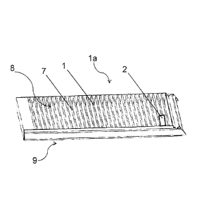
FIG 1 shows a filter element la, including a base body 1, whereby a sensor 2
is positioned
on the base body 1.
FIG 2 shows that the sensor 2 includes at least one electronic chip 4 and at
least one sensor
chip 5, which are positioned within a functional volume 3 which is at most 4-5
mm long, at
most 2-3 mm wide, and at most 0.5-0.8 mm high.
The distance x is 5 mm, the distance y is 3 mm, and the distance z is 0.8 mm.
The electronic
chip 4 includes several analog and/or digital interfaces through which
different sensor chips
can be analyzed.
A wireless energy and/or data transfer occurs by way of the electronic chip 4
and the sensor
chip 5. This can be achieved through a radio interface or a plug-free
connection through
contacts.
CA 02956867 2017-01-31
8
The electronic chip 4 and the sensor chip 5 are positioned on a circuit board
6, which has a
larger surface area than the functional volume 3.
The base body 1 includes a folded filter medium 7, which has an inflow side 8
and an outflow
side 9, whereby the sensor chip 5 has such a high resolution that a pressure
difference
between the inflow side 8 and the outflow side 9 in the range of 10-500 Pa can
be captured.
The sensor chip 5 has a resolution of 5 Pa.
The filter medium is manufactured from a non-woven material. However, paper
can also be
used as the filter medium. Filter element la can have glued edge strips. The
edge strips
can include a foam seal. The filter elements la can be constructed as a
combination filter. A
combination filter filters particles and gaseous substances.
FIG 3 shows in a schematic view the sensor chip 5. The sensor chip 5 enables
detection of
a pressure difference in the range of 10-500 Pa. The sensor chip 5 can consist
of either a
convertor element 10 which converts a pressure difference into an electrical
signal or of a
convertor element 10 with a sensor front end 11.
The sensor chip 5 with a convertor element 10 and/or the sensor chip 5 with a
convertor
element 10 and a sensor front end 11, is in its totality manufactured in 180
nm CMOS
technology.
The sensor front end 11 can include electronics or can be constructed as such.
The convertor element 10 can be constructed as a transistor or resistor on a
silicone
membrane.
FIG 4 shows in a schematic view the electronic chip 4. The electronic chip 4
includes analog
and/or digital interfaces for connection to further sensors 12 or further
sensor chips. The
electronic chip 4 includes a sensor front end 13. The electronic chip 4
includes a
microcontroller for signal processing 14. The electronic chip 4 includes a
memory 15. The
electronic chip 4 includes an RFID front end 16 for a contact free supply
and/or for a supply
through a contact connection.
CA 02956867 2017-01-31
9
FIG 5 illustrates by way of a further sensor 2' that the electronic chip 4'
and the sensor chip 5'
are positioned side by side on a circuit board 6'. The electronic chip 4' and
the sensor chip 5'
are electrically conductively connected with one another through bonding wires
17.
FIG 6 illustrates by way of a further sensor 2", that the electronic chip 4"
and the sensor chip
5" are electronically conductively connected with another by way of a flip
chip connection
using contact mounds 18, namely so called "bumps".
In FIG 5 as well as in FIG 6, the sensor 5', 5" includes a membrane 19', 19"
and electronic
arrangements 20', 20" which may include oxide layers. The sensor chip 5', 5"
respectively
includes a silicone substrate 21', 21", into which a membrane 19', 19" is
etched which aside
from the convertor elements 10', 10", is free of electronic arrangements or
oxide layers.
The electronic chip 4', 4" and the sensor chip 5', 5" are positioned on the
circuit board 6', 6"
in which a passage 6'a, 6"a is formed, whereby the passage 6'a, 6"a is the
only fluid
conducting access to a volume 22', 22" which is formed by the circuit board
6', 6", the sensor
chip 5', 5" and a sealing collar 23', 23" surrounding the sensor chip 5', 5",
whereby a first
membrane surface 19'a, 19"a of the membrane 19', 19" is oriented towards the
volume 22',
22".
The electronic chip 4', 4" is adhesively connected. The electronic chip 4', 4"
also includes
electronic arrangements 20', 20". The volume 22', 22" is sealed only by the
circuit board 6',
6", the sensor chip 5', 5" and the sealing collar 23', 23" which surrounds the
sensor chip 5',
5".
Different pressures p1 and p2 are present on two different sides of the
membrane 19', 19".
The differential pressure between the sides can be measured with the sensor
2', 2" when the
two sides are sealingly separated from one another and the sensor 2', 2" is
suitably
positioned and sealingly supported, This is schematically illustrated by the
broken line.
The sealing collar 23', 23" preferably consists of a casting compound which
sealingly flows
even into small gaps.
CA 02956867 2017-01-31
FIG 7 shows in transparent view that the contacting mounds 18 surround a
membrane 19".
The contacting mounds 18 must be exactly positioned in such a way that the
sensor chip 5"
or the membrane 19" is evenly subjected to mechanical tension.
An interface between the sensor chip 5, 5', 5" and the electronic chip 4, 4',
4" can be located
5 within the functional volume 3.