Note: Descriptions are shown in the official language in which they were submitted.
CA 02957265 2017-02-03
WO 2016/023234 PCT/CN2014/084542
ELECTRONIC TOY WITH RADIAL INDEPENDENT CONNECTOR
AND ASSOCIATED COMMUNICATION PROTOCOL
BACKGROUND OF THE INVENTION
[00011 The present invention relates generally to an electronic toy, and
more
specifically to an electronic toy comprising a base unit and one or more
characters
(e.g., figurines or statuettes).
[0002] Toys generally provide entertainment while also enabling children to
learn about the world around them. Toys may take many different forms. A toy
may be simple such as a set of wooden blocks, or complex such as an electronic
tablet computer device. Regardless, a successful toy should be fun to play
with.
[0003] Given the prevalence of electronic devices in modern day society,
many
children have come to expect a certain level of interactive feedback from
their toys.
In light of this, many of today's toys include one or more electrical
components
which are designed to sense a child's actions and provide suitable feedback in
response. In particular, a toy may generate a suitable audible response when a
child presses a button. For example, the toy may say, "This is the letter A,"
when
the child presses a button marked with the letter A. However, such toys
typically
have a fixed or very limited number of responses to such actions of a child.
For
example, a toy may alternate between saying, "This is the letter A," and
"Alligator
starts with the letter A" in response to the child pressing a button marked
with the
1
CA 02957265 2017-02-03
WO 2016/023234 PCT/CN2014/084542
letter A. Due to such fixed nature, the child may quickly outgrow or otherwise
become bored with such toys.
BRIEF SUMMARY OF THE INVENTION
[0004] The present disclosure is directed to an electronic toy in the form
of an
expandable play set as well as associated methods, communication protocols,
and
tangible computer-readable media as shown in and/or described in connection
with
at least one of the figures, as set forth more completely in the claims. In
some
embodiments, the play set may provide an interactive response based upon which
characters (e.g. figurines or statuettes) are coupled to a base unit, which
base unit to
which characters are coupled, and/or to which connectors of the base unit
characters are coupled. A character may include circuitry that permits the
character to obtain an identifier (ID) for a connector of base unit to which
the
character is coupled. Such circuitry may also permit the character to identify
and
communicate with other characters that are also coupled to the base unit.
Based
upon such IDs, the character may generate or otherwise cause suitable
interactive
responses such as, for example, activating a motor in the base unit, turning
on a
light in the base unit and/or character, generating a suitable audible
response via an
audio speaker of the character (e.g. singing with other characters attached to
the
base unit), etc.
[00051 These and other advantages, aspects and novel features of the
present
invention, as well as details of an illustrated embodiment thereof, will be
more fully
understood from the following description and drawings.
2
CA 02957265 2017-02-03
WO 2016/023234 PCT/CN2014/084542
BRIEF DESCRIPTION OF SEVERAL VIEWS OF THE DRAWINGS
[0006] Embodiments are described herein by way of example and not by way of
limitation in the accompanying figures. For simplicity and clarity of
illustration,
elements illustrated in the figures are not necessarily drawn to scale. For
example,
the dimensions of some elements may be exaggerated relative to other elements
for
clarity. Further, where considered appropriate, reference labels have been
repeated among the figures to indicate corresponding or analogous elements in
the
figures.
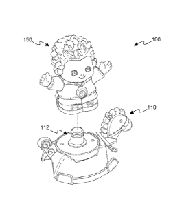
[0007] FIGS. 1A-1C show embodiments of an electronic toy in the form of an
expandable play set that includes one or more base units and one or more
characters to couple to the male connectors of the base units.
[0008] FIG. 2 illustrates further details regarding mating of the male
connectors
to female connectors of a character.
[0009] FIG. 3 illustrates further details of the female connector of a
character.
[0010] FIG. 4 provides a block diagram of electrical components found in an
embodiment of a character.
[0011] FIGS. 5A, 5B, and 5C depict differences between four, three, and two
contact connectors of a base unit.
[0012] FIGS. 6A, 6B, and 6C show other suitable cross-sections for the male
and
female connectors of the expandable toy set.
[0013] FIG. 7 provides a circuit diagram of connector interface circuitry
of a
character and connector interface circuitry of a base unit.
3
CA 02957265 2017-02-03
WO 2016/023234 PCT/CN2014/084542
[0014] FIG. 8 shows a flowchart of an ID detection process that may be
implemented by a character.
[0015] FIG. 9 illustrates a single data line, open drain network that may
be
formed by characters as a result of being attached to a base unit.
[0016] FIG. 10 provides various waveforms of signals generated by
characters of
an open drain network.
[0017] FIG. 11 illustrates an example master selection process that may be
implemented by the characters.
[0018] FIG. 12 illustrates example waveforms that may be generated by two
characters as a result of executing the master selection process of FIG. 11.
[0019] FIG. 13 illustrates a frame used by the characters to transmit and
receive
data via the open drain network of FIG. 9.
[0020] FIG. 14 illustrates a further details of a time slot of the frame
shown in
FIG. 13.
[0021] FIG. 15 illustrates an example order detection process that may be
implemented by a character that has assumed the role of master.
[0022] FIG. 16 illustrates an example order detection process that may be
implemented by a character that has assumed the role of slave.
DETAILED DESCRIPTION OF THE INVENTION
[0023] References in the specification to one embodiment", an embodiment",
an example embodiment", etc., indicate that the embodiment described may
include a particular feature, structure, or characteristic, but every
embodiment may
4
CA 02957265 2017-02-03
WO 2016/023234 PCT/CN2014/084542
not necessarily include the particular feature, structure, or characteristic.
Moreover,
such phrases are not necessarily referring to the same embodiment. Further, a
particular feature, structure, or characteristic described in connection with
an
embodiment generally may be incorporated into or otherwise implemented by
other embodiments regardless of whether explicitly described.
[0024] Referring now to FIGS. 1A-1C, embodiments of an expandable play set
100 are shown. In particular, FIG. 1A depicts a character 150 coupled to a
base
unit 110 that is shaped to resemble a rocking-horse. FIG. 1B depicts the
character
150 of FIG. 1A decoupled from a male connector 112 of the rocking-horse base
unit
110. FIG. 1C depicts a high level representation of another base unit 110 of
the
expandable play set 100 that includes two male connectors 112 that are
configured
to receive characters 150 such as the character 150 of FIGS 1A and 1C.
[00251 In general, the expandable play set 100 may include one or more base
units 110 and one or more characters 150. A base unit 110 may take the form of
a
vehicle (e.g., car, plane, scooter, bus, rocking-horse, amusement park ride),
a setting
(e.g. farm yard, country side, zoo, etc.), a building (e.g., a residence,
school, fire
station, police station, farm house, etc.) or some other locale with which a
child may
want to interact. As shown in FIGS. 1B and 1C, a base unit 110 may include one
or
more male connectors or connection points 112 to which characters 150 may be
mechanically and electrically detachably engaged or coupled. Further details
concerning male connectors 112 are presented below. Besides male connectors
112,
a base unit 110 may also include one or more loads such as a light emitting
diodes,
CA 02957265 2017-02-03
WO 2016/023234 PCT/CN2014/084542
motors, and/or other interactive devices that are electrically connected to
the male
connectors 112 via one or more wires not shown in FIGS. 1A-1C.
[0026] The characters 150 may also take a variety of forms. A character 150
may include an outer casing or housing 152 in the shape of a figurine or
statuette
that resembles a person (e.g., a boy, a girl, a zookeeper, a policeman, a
fireman, a
bus driver), an animal (e.g., a dog, cat, bear, cow, etc.), a robot, or some
other
personality, creature, etc. A depiction of a housing 152 in the shape of a boy
is
presented in FIG. 2.
[00271 Besides providing external aesthetic features of the character 150,
the
outer casing 152 may further provide a female connector 154 that is configured
to
mechanically engage a cylindrical post 114 of a male connector 112. Besides
mechanically engaging a male connector 112, the female connector 154 may
further
align terminals or pins 156 of the female connector 154 with annular contacts
116 of
the male connector 112. See, FIG. 3 for a depiction of the pins 156.
[0028] Referring now to FIG. 4, a block diagram of electrical components
found
in an embodiment of the character 150 is provided. As shown, the character 150
may include a processor 160, memory 162, and one or more input/output (I/O)
ports or interfaces 166. The processor 160, memory 162, and I/O ports 166 may
be
implemented using discrete components. However, in some embodiments, a
single chip microcontroller may implement the processor 160, memory 162, I/O
ports 166 or portions thereof.
6
CA 02957265 2017-02-03
WO 2016/023234 PCT/CN2014/084542
[0029] In some embodiments, one or more of the I/O ports 166 may include or
be associated with analog-to-digital converter (ADC) circuitry 167 that
converts
received analog signals to digital values suitable for processing by the
processor
160. Similarly, one or more of the I/O ports 166 may include or be associated
with
digital-to-analog converter (DAC) circuitry 168 that converts digital values
received
from the processor 160 to analog signals suitable for controlling and/or
communicating with other components. In some embodiments, the ADC and/or
DAC circuitry 167, 168 may be incorporated into I/O ports 166 of a
microcontroller.
In other embodiments, the ADC and/or DAC circuitry 167, 168 may be provided by
external components coupled to I/O ports 166 of a microcontroller.
[0030] The memory 162 may include both volatile memory 163 and non-volatile
memory 164. The non-volatile memory 164 may store instructions of a control
program to be executed by the processor 160. Via execution of the
instructions,
the processor 160 may control operation of the character 150 and the base unit
110.
As explained in greater detail below, the processor 160, as a result of
executing
instructions, may identify a male connector 112 to which the character 150 is
coupled, identify other characters 150 that are coupled to other male
connectors 112
of a base unit 110, control components of the base unit 110, control
components of
the character 150, and/or exchange data with other characters 150 via the base
unit
110.
[0031] Besides instructions of a control program, the non-volatile memory
164
may further include data used by the processor 160 such as audio clips to be
played
7
CA 02957265 2017-02-03
WO 2016/023234 PCT/CN2014/084542
back by the processor 160 through an audio speaker 174. In particular, the
non-volatile memory 164 may store one or more responses for each corresponding
ID of a male connector 112. As noted above, the memory 162 may be provided by
a microcontroller in some embodiments. In other embodiments, the memory 162
may be provided or partially provided by one or more components that are
external to a microcontroller. For example, the character 150 may include a
serial
peripheral interface (SPI) NOR flash device to store one or more responses
(e.g.,
audio clips, voice data, etc.) to be played back by the processor 160.
[00321 Details for obtaining the ID of a male connector 112 are present in
detail
below in regard to FIG. 8. Different characters 150 may have different
responses
for the same ID. Moreover, each character 150 may have more than a single
response for the same ID. Thus, coupling a first character 150 to a male
connector
112 of based unit 110 may generate a first set of responses from the first
character
150 where coupling a second character 150 to the same male connector 112 may
generate a second set of responses that differ from the first set of
responses.
[0033] In one embodiment, a play set 100 may be designed with approximately
147 different male connector IDs and each character 150 may be programmed with
over 400 responses. Moreover, the base units 110 and characters 150 of the
play
set 100 may be sold separately and/or packages (e.g., a base unit 110 and a
character
150). Furthermore, base units 110 and characters 150 of different packages may
be
mixed and matched. In other words, a character 150 sold in a first package may
be
used with a character 150 and base unit 110 sold in a second package in order
to
8
CA 02957265 2017-02-03
WO 2016/023234 PCT/CN2014/084542
provide new responses and interactions to the character 150 and base unit 110
of
the second package. In this manner, additional characters 150 and base units
110
may be added to characters 150 and base units 110 that a child already owns in
order to expand upon the play experience.
[0034] As shown, the character 150 may further include an electro-
mechanical
button 170 and associated LED 172 that are coupled to the processor 160 via
separate I/O ports 166. Via such I/O ports 166, the electro-mechanical button
170
may provide the processor 160 with a signal indicative of whether the button
170
has been pressed and the processor 160 may turn off and turn on the LED 172 as
appropriate. The character 150 may further include an audio speaker 174 and
interface circuitry 176. The audio speaker 174 may be coupled to the processor
160
via an I/O port 166 to permit the processor 160 to playback audio clips stored
in the
non-volatile memory 164 through the speaker audio 174. The connector interface
circuitry 176 may be coupled to the processor 160 via I/O ports 166 to permit
the
processor 160 to send and/or receive signals to and/or from the male connector
112.
Furthermore, the character 150 may include a battery compartment 180
configured
to receive one or more batteries 182 and align electrical terminals 184 of
such
batteries 182 with electrical contacts 186 of the battery compartment 180. As
such,
batteries 182 may be placed in the battery compartment 180 in order to deliver
electric power to the processor 160 and other electrical components of the
character
150 via electrical contacts 186.
9
CA 02957265 2017-02-03
WO 2016/023234 PCT/CN2014/084542
[0035] Turning now to FIG. 5A-5C, three embodiments of the male connectors
112 are shown. In particular, FIG. 5A depicts a four contact male connector
112a
in which four annular contacts 116a, 116b, 116c, 116d are positioned about a
cylindrical post 114a. FIG. 5B depicts a three contact male connector 112b in
which three annular contacts 116a, 116b, 116c are positioned about a
cylindrical
post 114b. FIG. 5C depicts a two contact male connector 112c in which two
annular contacts 116a, 116b are positioned about a cylindrical post 114c.
[0036] As noted above, the character 150 includes a cylindrical female
connector
154 configured to mechanically engage the cylindrical post 114 of a male
connector
112 and electrically couple pins 156 to the annular contacts 116. As explained
in
greater detail below, the cylindrical female connector 154 permits use of the
character 150 with male connectors 112 having different numbers of contacts
116
such as the four, three, and two contact embodiments of FIGS. 5A-5C.
[0037] In one embodiment, both the cylindrical female connector 154 of the
character 150 and the cylindrical posts 114 of the base units 110 have a
circular cross
section. The circular cross sections permit the characters 150 to be
mechanically
coupled to the male connectors 112 in a radially-independent manner. For
example, if the male connector 112 corresponds to a driver's seat of a
vehicle, the
character 150 may be mechanically coupled to the male connector 112 with the
character 150 facing forward, facing backward, facing to the left, facing to
the right,
or in any radially-facing direction in between.
CA 02957265 2017-02-03
WO 2016/023234 PCT/CN2014/084542
[0038] Besides permitting a mechanical coupling that is radially-
independent,
the structure of the male connectors 112 and the female connector 154 further
permit electrical coupling of the pins 156a, 156b, 156c, 156d to the
respective
contacts 116a, 116b, 116c, 116d in a radially-independent manner. As shown in
FIG. 3, each pin 156a, 156b, 156c, 156d has a longitudinal offset 158a, 158b,
158c,
158d from a base 153 of the character 150. Similarly, as shown in FIGS. 5A-5C,
each annular contact 116a, 116b, 116c, 116d has a corresponding longitudinal
offset
117a, 117b, 117c, 117d from a base 113 of the male connector 112. In
particular, the
longitudinal offsets 158a, 158b, 158c, 158d and corresponding longitudinal
offsets
117a, 117b, 117c, 117d are defined such that pins 156a, 156b, 156c, 156d
contact
corresponding annular contacts 116a, 116b, 116c, 116d when the character 150
is
fully seated on a male connector 112a.
[0039] In one embodiment, the Y+ annular contact 116a of each male
connector
112a, 112b, and 112c has a longitudinal offset 117a that roughly corresponds
to the
longitudinal offset 158a of a Y+ pin 156a of the female connector 154. As
such,
regardless to which male connector 112a, 112b, or 112c a character 150 is
coupled,
the female connector 154 and corresponding post 114a, 114b, 114c guides the Y+
pin
156a into contact with the Y+ annular contact 116a of the respective male
connector
112a, 112b, 112c. The pins 156b, 156c, 156d and annular contacts 116b, 116c,
and
116d operate in a similar manner; however, when the character 150 is coupled
to a
three contact male connector 112b, the Motor pin 156d remains unconnected as
male connector 112b does not include a corresponding Motor annular contact
116d.
11
CA 02957265 2017-02-03
WO 2016/023234 PCT/CN2014/084542
Similarly, when the character 150 is coupled to a two contact male connector
112c,
both the GND pin 156c and the Motor pin 156d remain unconnected as the male
connector 112c does not contain a corresponding GND annular contact 116c and a
corresponding Motor annular contact 116d.
[0040] As described above, in one embodiment, each character 150 in the
play
set 100 has a fixed number of pins 156 (e.g., four) and the base units 110 may
include male connectors 112 with two, three, and/or four contacts 116.
However,
the characters 150 in other embodiments may include a different number of pins
156. Moreover, the play set 100 may include characters 150 with a range of
pins
156 (e.g., characters 150 with two connectors as well as characters 150 with
four
connectors). Likewise, the male connectors 112 in some embodiments may all
have a fixed number (e.g., four) of annular contacts 116. Furthermore, the
play set
100 may reverse the position of the pins 156 and contacts 116 to where the
characters 150 include annular contacts 116 and the male connectors 112
include the
pins 156.
[0041] As noted above, the male connectors 112 and female connectors 154
may
each have a circular cross-section which permits coupling the characters 150
to the
male connectors 112 in a radially independent manner. Other embodiments may
forgo some radial independence by using male connectors 112 and female
connectors 154 with different shaped cross-sections. For example, both the
male
connector 112 and the female connector 154 may have an octagonal cross-section
that permits the character 150 to have eight different radial facings. See,
e.g., FIG.
12
CA 02957265 2017-02-03
WO 2016/023234 PCT/CN2014/084542
6A.
Radial independence, however, may be achieved or retained with
cross-sections other than circular. For example, as shown in FIG. 6B, radial
independence may be achieved via a female connector 154 having a square
cross-section and a post 114 of a male connector having a circular cross-
section.
Conversely, radial independence may also be achieved using a round female
connector 154 and a square post 114 as shown in FIG. 6C. In the embodiment of
FIG. 6B, a pin 156 may be placed on each side of the square female connector
154 to
engage an appropriate annular contact 116 of the post 114. In the embodiment
of
FIG. 6C, the female connector 154 may include annular contacts that engage
pins on
each side of the post 114.
[0042] FIG.
7 depicts details regarding aspects of an electrical interface between
the female connector 154 and four contact male connectors 112a. As shown, Y+,
AUX, GND, and Motor pins 156 and corresponding contacts 116 may electrically
couple interface circuitry 176 of a character 150 to connector interface
circuitry 119a
of a male connector 112a. As explained in detail below, the processor 160 of a
character 150 may identify a male connector 112a, control one or more aspects
of a
base unit 110, and communicate with other characters 150 via connector
interface
circuitry 119a, 176.
[0043] As
depicted, the interface circuitry 176, in one embodiment, includes
terminals I0A1, I0A4, I0A5, I0A6, I0A7, I0B0, I0B1, I0B2, I0B3, X-, and X+.
Each such terminal may be coupled to processor 160 via a corresponding I/O
port
13
CA 02957265 2017-02-03
WO 2016/023234 PCT/CN2014/084542
166. As such, the processor 160 may read a voltage from and/or apply a voltage
to
such terminals via the respective I/O ports 166.
[0044] The I0A1 terminal is coupled to the drain of transistor Q7 via
resistor
R22. The Motor pin 156d is coupled to the collector of transistor Q3, the
drain of
transistor Q6, and the gate of transistor Q7. The I0B2 terminal is also
coupled to
the drain of the Q6 transistor and the gate of transistor Q7 via the diode D2
and the
resistor R23. The I0A4 terminal is coupled to the gate of transistor Q6, and
the
source of transistor Q6 is coupled to ground. The I0A6 terminal is coupled to
the
base of transistor Q3 via resistor R11 and the emitter of transistor Q3 is
coupled to
power source VDD.
[00451 The X- terminal is coupled to the AUX pin 156b. The X+ terminal is
coupled to the Y+ pin 156a via resistor R3. The IOBO terminal is coupled to
the Y+
pin 156a, and the I0B3 terminal is coupled to the AUX pin 156b via resistor
R42.
The AUX pin 156b is further coupled to power source VDD via pull-up resistor
R6.
[0046] The I0B1 terminal is coupled to the base of transistor Q2 via
resistor R15.
Similarly, I0A7 is coupled to the base of transistor Q5 via resistor R2. The
emitter
of transistor Q2 and the emitter of transistor Q5 are coupled to power source
VDD.
The collector of transistor Q2 is coupled to the AUX pin 156b, and the
collector of
transistor Q5 is coupled to the AUX pin 156b via resistor R17.
[00471 Referring now to connector interface circuitry 119a, the Y+ contact
116a is
coupled to resistor R31, which is coupled to light-emitting diode LED1,
resistor R30,
and AUX connector 116b. Resistor R30 is further coupled to ground via a first
14
CA 02957265 2017-02-03
WO 2016/023234 PCT/CN2014/084542
path through key K2 and a second path via resistor R33. Similarly, light-
emitting
diode LED1 is further coupled to ground via a first path that includes
resistors R29
and R33 and a second path that includes resistor R29 and key K2.
[0048] The Motor contact 116d is coupled to the GND contact 116c via
light-emitting diode LED2 and resistor R47. The Motor contact 116d is further
coupled to the drain of transistor Q12 via a load such as motor MOTOR. The
Motor contact 116d is also coupled to a data line of the communication
interface 120.
The gate of transistor Q12 is also coupled to the data line via a resistor R43
and to
GND contact 116c via capacitor C26. The data line is further coupled to the
GND
contact 116c via a first path that includes pull-down resistor R28 and a
second path
that includes key K1 and resistor R20.
[0049] As explained above in regard to FIG. 5C, the two contact male
connector
112c does not include GND and Motor contacts 116c, 116d. As such, the
connector
interface circuitry 119c of the two contact male connector 112c may include
only a
subset of the components found in the connector interface circuitry 119a which
may
reduce implementation costs. In particular, connector interface circuitry 119c
may
merely include resistor R31 coupled between the Y+ and AUX contacts 116a, 116b
as indicated by the dotted-line box labeled 119c in FIG. 7.
[00501 Similarly, the three contact male connector 112b does not include a
Motor
contact 116d. A such, the connector interface circuitry 119b of the three
contact
male connector 112b may include only a subset of the components found in the
connector interface circuitry 119a which may reduce implementation costs. In
CA 02957265 2017-02-03
WO 2016/023234 PCT/CN2014/084542
particular, the connector interface circuitry 119b may include resistor R31 as
well as
resisters R29, R30, R33, light-emitting diode LED1, and key K2 as indicated by
the
dotted-line box labeled 119b in FIG. 7.
[00511 Referring now to FIG. 8, a ID detection process 200 used by the
processor
160 of a character 150 is shown. In general, the male connectors 112 identify
themselves based on resistors R28, R30, R31 which in essence provide the male
connectors 112 with identification circuitry. In particular, the combination
of
resistance values for resistors R28, R30, R31 may be varied among male
connectors
112 in order to unique identify male connectors 112. The processor 160 may
apply
voltages to contacts 116 of the male connectors 112 in order to generate
voltage
levels that are dependent upon the resistors R28, R30, R31 and thereby
identify a
male connector 112 based on the generated voltages.
[00521 To this end, the processor 160 at 210 may set the I0B2 terminal and
the
I0A1 terminal to the predetermined high voltage VHIGH. As a result of applying
the high voltage VHIGH to terminal I0B2 and terminal I0A1, a voltage Vi is
developed at terminal I0A5 that is dependent upon a resistance of resistor
R28. In
one embodiment, if resistor R28 has a resistance of 100 KO, then a voltage is
developed at the gate of transistor Q7 sufficient to turn on and connect the
terminal
I0A5 to ground. Conversely if resistance of the resistor R28 is 0 0, the
transistor
Q7 remains off and the terminal I0A5 is pulled to the high voltage VHIGH by
resistor
R22. Accordingly, the terminal I0A5 provides the processor 160 with a logic
high
or "1" value when resistor R28 is 0 0 or otherwise sufficiently low to prevent
16
CA 02957265 2017-02-03
WO 2016/023234 PCT/CN2014/084542
turning on the transistor Q7 or a logic low or "0" value when the resistor R28
is 100
KO or sufficiently high to turn on the transistor Q7. If the resistor R28 is
not
present (e.g., two or three contact male connectors 112b, 112c), resistor R28
effectively is a very large resistance. As such, setting the I0B2 and I0A1
terminals
to the high voltage VHIGH will turn on transistor Q7 and provide a logic low
value to
the I0A5 terminal. At 220, the processor 160 may read the voltage Vi developed
at the I0A5 terminal to obtain a value indicative of the resistance of
resistor R28.
[00531 After obtaining a value for voltage Vi, the processor 160 at 230 may
set
the X+ terminal to a predetermined high voltage VHIGH (e.g. VDD) and the X-
terminal to predetermined low voltage VLow (e.g., OV). As a result of applying
such voltages to the X+ terminal and the X- terminal, a voltage V2 is
developed at
the IOBO terminal that is dependent upon the resistance of resistor R31 in the
male
connector 112 to which it is attached. At 240, the processor 160 may read the
voltage V2 developed at the Y+ terminal to obtain a value indicative of the
resistance of resistor R31.
[00541 After obtaining a value for voltage V2, the processor 160 at 250 may
set
I0A7 to a predetermined low voltage VLow to turn on transistor Q5. As a result
of
turning on transistor Q5, a voltage V3 is developed at the AUX pin 156b that
is
dependent upon the resistance of resistor R30 if present. At 260, the
processor 160
may read the voltage V3 developed at the X- terminal to obtain a value
indicative of
the resistance of resistor R30. Even if the resistor R30 is not present (e.g.,
a two
contact male connector 112c), the developed voltage V3 is still indicative of
the
17
CA 02957265 2017-02-03
WO 2016/023234 PCT/CN2014/084542
absence of resistor R30. In other words, the processor 160 may detect the
absence
of the resistor R30 based on the voltages V2 and V3.
[0055] Finally, the processor 160 at 270 may obtain an identifier (ID) for
the male
connector 112 based upon the obtained values Vi, V2, V3. In one embodiment,
interface circuitry 176 and connector interface circuitry 119a, 119b, 119c
essentially
generate a binary value for value Vi, but generate analog values V2, V3 that
are
subsequently digitized by corresponding 10 ports 166. As such values V2 and V3
are likely to vary a bit between readings and between different male
connectors 112
that are supposed to have the same ID. As such, the processor 160 may obtain
an
ID for a male connector 112 based upon associated ranges for values V2 and V3.
For example, the processor 160 may obtain an ID for a male connector 112 that
is
associated with a four contact male connector 112a on a base unit 110 known to
be
shaped as an airplane if value Vi is a logical high value, value V2 is between
values
digital values X and Y and value V3 is between digital values A and B. The
processor 160 may use the obtained ID to retrieve an appropriate response from
its
memory 162 and may execute the retrieved response. For example, the processor
160 may cause the character 150 to playback an audio clip that says "I enjoy
flying
my plane," or may cause detected base unit 110 to generate an appropriate
response such as turn on a motor that slowly rotates a propeller of the plane.
[0056] As explained above, the processor 160 may obtain an ID of a male
connector 112. As such, the processor 160 may ascertain whether the male
connector 112 to which its character 150 is attached is a four, three, or two
contact
18
CA 02957265 2017-02-03
WO 2016/023234 PCT/CN2014/084542
male connector 112a, 112b, 112c. As noted above, the two contact male
connector
112c may merely provide a resistor R31 for identification purposes. As such,
the
processor 160 with respect to two contact male connectors 112c merely
identifies
the point 112c and generates an appropriate response. However, four and three
contact male connectors 112a, 112b enable additional functionality.
[0057] As noted above, the four and three contact male connector 112a, 112b
may include a key K2 and a light-emitting diode LED1. To sense the state of
the
key K2, the processor 160 may set the I0A7 terminal to a low voltage level
\how.
In such a configuration, transistor Q5 turns on and pulls the X- terminal to a
high
voltage level VHIGH if key K2 is not pressed. However, if key K2 is pressed,
resistors R17 and R30 form a voltage divider which reduces the voltage
developed
at the X- terminal to a value less than the high voltage level VHIGH.
Accordingly,
the processor 160 may sense whether the key K2 is pressed by monitoring the
value
of the X- terminal when the I0A7 terminal is set to a low voltage level \how.
[0058] To control the light-emitting diode LED1, the processor 160 may turn
on
transistor Q2 by setting the I0B1 terminal to a low voltage level VLow such as
ground. Turning on transistor Q2 connects the light-emitting diode LED1 to a
high voltage level VHIGH such as VDD which causes the light-emitting diode
LED1
to illuminate. Conversely, the processor 160 may turn off the transistor Q2 by
setting I0B1 to a high voltage level VHIGH which causes the light-emitting
diode
LED1 to turn off. As such, the processor 160 may turn on and off the
light-emitting diode LED1 as appropriate via the I0B1 terminal.
19
CA 02957265 2017-02-03
WO 2016/023234 PCT/CN2014/084542
[00591 The four point male connector 112a may further include a key K1 and
a
light-emitting diode LED2. To sense the state of the key K1, the processor 160
may
set the I0B2 terminal to a high voltage level VHIGH. In such a configuration,
transistor Q7 turns on thus pulling the I0A5 terminal to ground if the key K1
is not
pressed. However, if key K1 is pressed, transistor Q7 turns off thus pulling
the
I0A5 terminal to a high voltage level VHIGH. Accordingly, the processor 160
may
sense whether the key K1 is pressed by monitoring the value of the I0A5 when
the
I0B2 terminal is set a high voltage level VHIGH. In one embodiment, the
processor
150 may only detect the status of K1 when the load MOTOR is not turned on.
[0060] To control the light-emitting diode LED2, the processor 160 may turn
on
transistor Q3 by setting I0A6 terminal to a low voltage level VLow such as
ground.
Turning on transistor Q3 connects the light-emitting diode LED2 to a high
voltage
level VHIGH such as VDD which causes the light-emitting diode LED2 to
illuminate.
Conversely, the processor 160 may turn off the transistor Q3 by setting I0A6
to a
high voltage level VHIGH which causes the light-emitting diode LED2 to turn
off.
As such, the processor 160 may turn on and off the light-emitting diode LED2
as
appropriate via the I0A6 terminal. In one embodiment, the load MOTOR cannot
be used when using LED2.
[0061] In one embodiment, the base unit 110 includes wires that couple the
communications interface 120 of each male connector 112a together. In
particular,
the base unit 110 may include a wire or wires that couple the data lines of
each
communications interface 120 together. Similarly, the base unit 110 may
include a
CA 02957265 2017-02-03
WO 2016/023234 PCT/CN2014/084542
wire or wires that couple ground of each communications interface 120
together. As
a result of such interconnection of male connectors 112a, the transistors Q6
and
associated pull-up transistors R23 of the characters 150 effectively create a
open
drain network of FIG. 9 when multiple male connectors 112a of a base unit 110
have
characters 150 coupled thereto.
[0062] As explained in greater detail below, the processor 160 may
therefore
utilize the Motor pin 156d to communicate with other characters 150 using a
bi-directional serial communications protocol over a single data line that is
shared
by the other characters 150. To this end, the processor 160 may use the I0A5
terminal associated with transistor Q7 as a DATA IN terminal to receive data
from
other characters 150. Similarly, the processor 160 may use the terminal I0A4
associated with transistor Q6 as a DATA OUT terminal to transmit data to other
characters 150.
[0063] Besides using the Motor pin 156d for communication, the processor
160
may further control a load such as motor MOTOR via the Motor pin 156d. In
particular, the processor 160 may turn on the load by turning the transistor
Q3 on
via terminal I0A6. More specifically, the processor 160 may set the terminal
I0A6
to a low voltage level VLow to turn on transistor I0A6 which causes the
capacitor
C26 to charge up. After a short while, the capacitor C26 may be sufficiently
charged to turn on the transistor Q12 and thereby turn on a load such as the
motor
MOTOR. Conversely, to turn off the load, the processor 160 may turn off the
transistor Q3 by applying a high voltage VHIGH via terminal I0A6.
21
CA 02957265 2017-02-03
WO 2016/023234 PCT/CN2014/084542
[00641 Since the Motor pin 156d is used for both communication and control
of a
load, the processor 160 uses a network or communications protocol that is
defined
in such a manner that prevents unintended turning on of the load. As noted
above, the capacitor C26 turns on the load a short while after the MOTOR
contact
116d has been at a high level VHIGH. As such, the networking protocol, in one
embodiment, is designed to ensure that the Motor contact 116d does not remain
at
the high level VHIGH for a time sufficient to turn on the load. More
specifically, the
capacitance of capacitor C26 affects the delay period or charging period
required to
turns on load. As such, the capacitance of capacitor C26 is selected to ensure
there
is not too much delay before turning on the load while at the same time
ensuring
that the charging period is sufficient to prevent communications via the Motor
pin
156d from inadvertently turning on the load. In one embodiment, the
capacitance
of the capacitor C26 is selected such that the capacitor C26 turns on the load
when
the Motor contact 116d is held high for roughly 20 to 40 symbol times.
[00651 To this end, the network protocol implemented by the processors 160
of
the characters 150 use signals in accordance with those depicted in FIG. 10.
As
explained in detail below, generally one of the characters 150 attached to the
network has the role of master and the other characters 150 attached to the
network
have the role of slaves. During idle periods, the master pulls the data line
to a low
level Wow. As such, if the data line is low for more than a symbol time as
shown
at 310 (e.g., at least 125% of a symbol time), then a master exists. However,
if the
data line is high for more than a symbol time as shown at 320, then a master
does
22
CA 02957265 2017-02-03
WO 2016/023234 PCT/CN2014/084542
not exist. Besides reflecting presence or absence of a master, the data line
may be
further used to transmit a data bit or symbol. To this end, a master device
(e.g., a
character 150) may transmit data using a symbol coding scheme similar to
Manchester coding. In particular, the master may transition the data line from
a
high level VHIGH to a low level \how to transmit a data "1" as shown at 330.
Conversely, the master may transition the data line from a low level \how to a
high
level VHIGH to transmit a data "0" as shown at 340. In one embodiment, the
processors 160 may cause such transitions to occur at roughly the center of a
symbol time period. As such, for a data "1", the data line may be at the high
level
VHIGH for the first half of the symbol time and may be at the low level \how
for the
second half of the symbol time period. Conversely, for a data "0", the data
line
may be at the low level \how for the first half of the symbol time period and
may be
at the high level VHIGH for the second half of the symbol time period. An
example
waveform is provided at 350 in which a master is first advertised followed by
the
transmission of data bits 1, 1, 1, 0, 0, 1.
[0066] Referring now to Figs. 11 and 12, a master selection process 400
that may
be implemented by the processors 160 to select a master will be described. In
particular, FIG. 11 depicts a flowchart of the master selection process 400
that may
be implemented by each processor 160. FIG. 12 depicts example waveforms on
the open drain network as a result of two characters 150 (e.g., Device A and
Device
B) both attempting to become a master.
23
CA 02957265 2017-02-03
WO 2016/023234 PCT/CN2014/084542
[00671 The following description uses phrases such as "the processor 160
permitting the data line to go or float high," "the processor 160 pulling the
data line
low," and similar phrases. Such phrases are used as a matter of convenience.
More accurately, the processor 160 generates signals for terminal I0A4 which
turn
on or turn off transistor Q6 which in turn cause the transistor to
respectively pull
the data line low via Motor pin 156d or permit the pull-up resistor R23 to
pull the
data line high via Motor pin 156d. Such verbosity would obscure the nature of
the
following disclosure and the above phrases capture the essence of the
processor 160
controlling the resulting pulling up and down of the data line. Similarly, the
processor 160 may determine the status of the data line based on signals
obtained
via transistor Q7 and the I0A5 terminal. Again, this concept is captured below
as
the processor 160 reading or determining the state of the data line despite
the fact
that the processor 160 may obtain such information via other components such
as
transistor Q7, the I0A5 terminal, and associated I/O port 166.
[0068] At 410, a processor 160 may determine whether no master is present
based on the status of the data line. As noted above, a master pulls the data
line
low and if no master is present the open drain nature of the network results
in the
data line being pulled high. Thus, if the data line is high for longer than a
symbol
time, then the processor 160 at 410 may determine that no master is present.
However, if the data line is low or has not been high for more than a symbol
time,
then the processor 160 may return to 410 to further assess whether a master is
present. In this manner, the processor 160 may continually monitor the network
24
CA 02957265 2017-02-03
WO 2016/023234 PCT/CN2014/084542
for the presence of a master and may attempt to become a master if no master
is
present.
[0069] As shown during period Ti in FIG. 12, the network has been high for
more than a symbol period and such status has been read by both Devices A and
B.
As such, both Devices A and B may detect at 410 that no master is present and
may
proceed to 420 in an attempt to become master. At 420, the processor 160 may
pull
the data line low for a short period of (e.g., 4 ms). This short period of
being
pulled low may reduce the number of devices competing to become the master
since not all devices on the network may detect the absence of a master at the
same
time. In particular, later devices may detect the line pulled low during their
monitoring at 410 and thus not proceed to 420. The short period of 420 is
reflected
in FIG. 12 as period T2.
[00701 At 430, the processor 160 may clear a counter C. At 440, the
processor
160 may randomly select a time slot value between 0 and a maximum number of
time slots MAX ¨ 1 and continue to hold the data line low for the randomly
selected
number of time slots. For example, the protocol may utilize 32 time slots each
having a period of 16 ms. The processor 160 may randomly select a value
between
0 and 31 and hold the data line low for the selected number of time slots.
Thus, if
the processor 160 selected the number 5, then the processor 160 may continue
to
hold the data line low for an additional 5 time slots or 80 ms in such an
embodiment. This random period of being held low is shown as period T3 in FIG.
CA 02957265 2017-02-03
WO 2016/023234 PCT/CN2014/084542
12. Of
particular note, FIG. 12 depicts that Device A has selected a larger time slot
value than Device B and thus holding the data line low for a longer period T3.
[00711
After holding the data line low based on its randomly selected time slot
value, the processor 160 at 450 may determine whether another device is
competing
for the role of master. To this end, the processor 160 at 450 may stop pulling
the
data line low for a short period of time and read the status of the data line.
If data
line is low, that means another device is competing for the role of master. As
such,
the processor 160 may return to 410, thus giving up its current attempt to
become
master. However, if the data line is high, then another device is not
competing for
the role of master. Accordingly, the processor 160 at 460 increments its
counter C
and immediately pulls the data line down to further its pursuit of the role of
master.
In one embodiment, the short period of time to read the state at 450 is less
than 5%
of the time slot period in order to reduce the likelihood of other devices
mistakenly
detecting that no other device is competing for the role of master. As shown
in
FIG. 12, the Device B at period T4 detects that the data line is low and
therefore
another device is trying to become master. As a result, the Device B may
return to
410 and cease its current pursuit of becoming the master. Device A, however,
at
period T4 detects that the data line is high and therefore that no other
device is
trying to become master. As such, the Device A increments its counter C and
pulls
the data line low at 460.
[00721
After incrementing the counter C, the processor 160 at 470 determines
whether the counter C has reached a predetermined number (e.g., 3). If the
26
CA 02957265 2017-02-03
WO 2016/023234 PCT/CN2014/084542
counter C has reached the predetermined count, then the processor 160 has
successfully detected that no other device is trying to become master a number
of
times equal to the predetermined count. Accordingly, the processor 160 may
proceed to 480 where the processor 160 may assume the role of master. However,
if the counter C has not reached the predetermined count, then the processor
160
may return to 440 to select another random time slot value and repeat the
process
until the processor 160 either (i) ceases its pursuit of becoming master as a
result of
detecting another device attempting to become master at 450, or (ii) obtains
the
predetermined count C and proceeds to 480 to assume the role of master.
[00731 From the above, it should be appreciated that the master selection
process is accomplished via a few short pulses. As such, the total time to
complete
the master selection process may be much shorter than a predefined training
sequence found in other protocols. Moreover, the total time may also be
shorter
than the time to transmit a packet containing many bits found in other
protocols.
As such, the master selection process of FIG. 12 may enable a quick master
resolution thus permitting master and slave devices to quickly respond to
changes
in the network configuration. More specifically, a child may repeatedly
attach,
detach, reattach, reorder, etc. the position of characters 150 with respect to
male
connectors 112 of a base unit 110. Quick resolution of the network
organization
(i.e., which characters 150 at any given time are master or slave) is desired
so that
the characters 150 may quickly provide a suitable interactive response to the
child's
actions.
27
CA 02957265 2017-02-03
WO 2016/023234 PCT/CN2014/084542
[0074] Referring now to FIG. 13, a frame 500 used by the master and slaves
for
bi-directional communication is shown. As shown, the frame 500 includes a
preamble 510 from master, a start bit 520 from master, M data bits 530 from
master,
a parity bit 540 from master, and N reply bits 550 from slave. In one
embodiment,
M and N are 6 and the preamble 410 corresponds to the master pulling the data
line
low for more than a symbol period. Due to the open drain implementation of the
network, if there is no reply from the slave device, the network signal for
the reply
period 550 would float high and inadvertently turn on the load (e.g., motor
MOTOR). To address this, each reply slot of the reply period 550 is
implemented
as shown in FIG. 14.
[0075] At the start of the reply slot, the master device pulls up the data
line for a
short period of time (e.g., 0.1% of the time slot) as shown as period Ti in
FIG. 14.
The slave device(s) may derive the timing from the falling edge of the period
Ti
pulse for synchronization. The master device continues to pull down the data
line
during period T2. During the period T3 which corresponds to roughly 25% to 75%
of the time slot, the slave device provides a reply value. In particular, if
the reply
is a data "0", the slave pulls the data line low during period T3. Conversely,
if the
reply is a data "1", then the slave does not pull the data line low during
period T3.
[0076] At 50% of the time slot, the master may read the data line to obtain
the
reply bit from the slave. As shown, the master during period T4 may cease
pulling down the data line. As such, the data line achieves the reply value
28
CA 02957265 2017-02-03
WO 2016/023234 PCT/CN2014/084542
provided by the slave. Thus, the master at 50% of the reply slot may then read
the
data line to obtain the reply bit from the slave.
[00771 FIG. 14 should make it readily apparent that the master pulls the
data
line low for all but a few brief periods (e.g., periods Ti and T4 of the reply
slot).
As such, the master ensures that the load is not inadvertently turned on. In
addition to the waveform shown in FIG. 14, the master may perform collision
detection during the start bit 520, M data bits 530, and parity bit 540. In
particular,
the master may ascertain whether it is able to successfully pull the data line
high
before each falling edge. If master is unable to successfully pull the data
line high
before each falling edge, then the master detects a data collision. In
response to
detecting a data collision, the master continues sending the remaining bits of
the
frame. The master may relinquish the master role and then attempt to regain
the
master role via the master selection process 400 described above in regard to
FIG.
11.
[00781 Some play scenarios of the play set 100 detect the order in which
characters 150 are coupled to the male connectors 112d and thus added to the
network. The characters 150 may then provide interactive responses based on
such detected order. To this end, an order detection process 400 is shown in
FIG.
15. In some embodiments, the master is not necessarily the first character 150
to
be added to the network. Instead, each character 150 having the role of master
implements the order detection process 600 shown in FIG. 15, and each
character
29
CA 02957265 2017-02-03
WO 2016/023234 PCT/CN2014/084542
having the role of slave implement the order detection process 700 shown in
FIG.
16.
[00791 As explained above in regard to FIG. 11, the characters 150 may
implement the master selection process 400 and assume the role of master at
480.
Upon becoming a master, the processor 160 of such character 150 at 610 of FIG.
15
may initialize a counter K to zero and send a first polling packet at 620. At
630,
the processor 160 may determine whether a response to the first polling packet
has
been received. If a response has not been received, the processor 160 may
increment the counter K at 640. At 650, the processor may determine whether a
predetermined number (e.g. 3) of first polling packets have been sent. In
particular, if the counter K equals the predetermined number (e.g. 3), then
the
processor 160 may determine that the predetermined number have been sent. As
such, the processor 160 at 660 determines that its character 150 is the first
device
coupled to the network. The processor 160 at 670 then proceeds with normal
communications. Otherwise, the process 160 returns to 620 to send another
first
polling packet.
[0080] If the processor 160 at 630, however, receives a response to a first
polling
packet, then the processor 160 at 680 determines that its character 150 was
not the
first character 150 attached to the network. More specifically, the processor
160 at
680 proceeds as if its character 150 was the second character 150 attached to
the
network. The processor 160 then at 670 proceeds with normal communications.
CA 02957265 2017-02-03
WO 2016/023234 PCT/CN2014/084542
[0081] As explained above in regard to FIG. 11, the characters 150 may
cease
pursuit of the role of master and become a slave. Upon becoming a slave, the
processor 160 may execute the order detection process 700 to ascertain the
order
devices are connected to the network. In particular, the processor 160 at 710
may
determine that its character 150 by default is the second character to attach
to the
network. However, if the processor 160 at 720 receives a first polling packet,
the
processor 160 at 730 sends a reply to the first polling packet. Moreover, the
processor 160 at 740 determines its character 150 is the first character 150
attached
to the network.
[0082] A few examples of play flow are presented in order to aid in further
understanding of how the base units 110, characters 150, and communications
protocol are intended to interact in one embodiment. In particular, two
characters
150 via the base unit 110 and communications protocol may talk to each other,
answer simple questions, and sing together. Such singing may take different
forms such as singing in parts, synchronized singing together, singing alone,
etc.
Moreover, while the characters 110 talk and otherwise interact with one
another,
the characters 110 may active various interactive devices or loads of the base
unit
110 such as, for example, light-emitting diodes and motors.
[0083] Example A: Singing in parts
Dylan: "Hi, I'm Dylan."
Maddie: "I'm Maddie."
Dylan: "Let's sing together!"
31
CA 02957265 2017-02-03
WO 2016/023234 PCT/CN2014/084542
Maddie: "Ha ha! I'd love to!"
Dylan: "I've got my friends! Its time to play!" (Part A of the song)
Maddie: "Let's learn and share and sing today!" (Part B of the song)
[00841 Example B: Synchronize singing together
Dylan: "Hi, I'm Dylan."
Maddie: "I'm Maddie."
Dylan: "Do you want to sing with me?"
Maddie: "Alright! "
Dylan + Maddie: "I've got my friends! Its time to play! Let's learn and
share and sing today!" (sing together)
[00851 Example C: Singing alone
Dylan: "Hi, I'm Dylan."
Maddie: "I'm Maddie."
Dylan: "Can you sing for me?"
Maddie: "Alright!"
Maddie: "I'm Maddie! I love my rocking horse, I'm always ready to
ride, of course." (Maddie's own song)
[00861 Various embodiments of the invention have been described herein by
way of example and not by way of limitation in the accompanying figures. For
clarity of illustration, exemplary elements illustrated in the figures may not
necessarily be drawn to scale. In this regard, for example, the dimensions of
some
32
CA 02957265 2017-02-03
WO 2016/023234 PCT/CN2014/084542
of the elements may be exaggerated relative to other elements to provide
clarity.
Furthermore, where considered appropriate, reference labels have been repeated
among the figures to indicate corresponding or analogous elements.
[0087] Moreover, certain embodiments may be implemented as a plurality of
instructions on a non-transitory, computer-readable storage medium such as,
for
example, flash memory devices, hard disk devices, compact disc media, DVD
media, EEPROMs, etc. Such instructions, when executed by processor 160, may
result in the character 150 implementing various previously described methods
and
processes.
[0088] While the present invention has been described with reference to
certain
embodiments, it will be understood by those skilled in the art that various
changes
may be made and equivalents may be substituted without departing from the
scope
of the present invention. In addition, many modifications may be made to adapt
a
particular situation or material to the teachings of the present invention
without
departing from its scope. Therefore, it is intended that the present invention
not
be limited to the particular embodiment or embodiments disclosed, but that the
present invention encompasses all embodiments falling within the scope of the
appended claims.
33