Note: Descriptions are shown in the official language in which they were submitted.
CA 02957486 2017-02-07
WO 2016/034883
PCT/GB2015/052547
- 1 -
Scalable Architecture for Digital Signal Processing
Field of the Invention
The present invention relates to an architecture for digital signal
processing, and
particularly, but not exclusively to a fully scalable architecture for on-
board satellite
digital signal processing.
Background of the Invention
The use of on-board digital processing to provide real time signal processing
is
io becoming increasingly widespread in satellites for telecommunications,
Earth
observation, science and navigation applications. Rapid advances in the
underlying
semiconductor technologies are bringing increasingly ambitious digital
processing
applications within the realms of feasibility.
A typical digital processing system used in a satellite is shown in Figure 1.
The system
takes in a number N1n of analogue signal inputs and generates a number Now of
analogue output signals, managed by a control system with access to ground
telecommand and telemetry links. The input signals must be digitized in order
to be
processed numerically and this involves a stage of analogue signal
conditioning or "pre-
processing" followed by analogue-to-digital (A/D) conversion. Similarly,
generation of
each output signal involves a stage of digital-to-analogue (D/A) conversion
followed by
analogue "post-processing".
Generation of each output signal in general requires information from any or
all of the
input signals, which means that the digital signal processing function does
not
decompose simply into what will be referred to as "horizontal slices" (in the
sense of a
horizontal pathway through the system diagram, representing a 1:1 mapping
between
an input and a respective output) or processing chains but must provide cross-
connections between all inputs and outputs. Both input and output signals may
be
continuously active and therefore the digital signal processing must also be
capable of
operating continuously and in real time at a rate commensurate with the signal
bandwidth. Increasing the scale of the system by adding more inputs
and outputs increases the processing load proportionately but the amount of
cross-
connection required may increase more substantially, in some cases in
proportion to
the product Nin x Nout.
CA 02957486 2017-02-07
WO 2016/034883 PCT/GB2015/052547
- 2 -
Digital systems for use on board a spacecraft face additional challenges
beyond those
normally experienced by terrestrial systems, and consequently, the cost of
qualification
of new technology for space flight can be very high. A first necessity for the
digital
processor is to survive its journey into orbit, for which it must be enclosed
in a suitable
mechanical housing to withstand the severe vibration and shock levels
experienced
during launch. Once in orbit it must operate continuously and reliably for
many years
without maintenance. Stress relief measures must be implemented at all
internal
interfaces to ensure that sensitive electronic components and assemblies
withstand all
the mechanical stresses experienced within the satellite environment. The
design must
io also cater for potentially large amounts of heat dissipated by the
processor, which must
be efficiently removed from the processor to maintain a safe operating
temperature.
This has to occur primarily by conduction through the metal housing since the
on-
board processor operates in a vacuum.
/5 The most common engineering solution is to place the processor in a
large metal box
comprising a back-plane and a set of daughter cards. The box provides a strong
mechanical structure, an interface to the spacecraft's thermal management
systems and
some shielding against ionizing radiation. The main processing components are
located
on the daughter cards, with interconnects between these occurring via
20 the backplane. The printed circuit board technology used for both
daughter cards and
back-plane support high density tracks for interconnect, but the provision of
suitably
robust connectors and the cross-connection of large quantities of interconnect
on the
back-plane are challenging. This cross-connection is particularly important
for a digital
channelizer and router, for example, whose main function is to provide a very
high
25 capacity interconnect with as much flexibility as possible between a
large number of
input and output ports. This implies a very large number of tracks which must
cross
each other and this can be difficult to manage within the two-dimensional
confines of
printed circuit board technology while maintaining signal integrity.
30 The principal disadvantage of the back-plane solution is that is not
fully scalable and
therefore not ideally optimised to all mission sizes. Specifically, the box
and the back-
plane printed circuit board must be re-designed and re-qualified for different
mission
sizes, or else the largest scale box must be used for all missions, which is
inefficient
within a severely mass-constrained payload.
CA 02957486 2017-02-07
WO 2016/034883 PCT/GB2015/052547
- 3 -
For a satellite system such as an on-board digital channelizer, which
processes uplink
beam signals, separates out the wanted channels from interference, and
rearranges and
routes just the wanted channels for retransmission on appropriate downlink
beams and
frequencies, the number of cross-connections which are required is usually
high.
Accordingly, this can be difficult to achieve using a back-plane solution
where all the
interconnections must be routed within a printed circuit board. In order to be
processed digitally, the radio frequency input signals are first filtered and
down-
converted in frequency to provide a band-limited signal suitable for analogue-
to-digital
conversion. Each signal corresponds to a relatively wide frequency band
segment from
io an uplink beam (or antenna feed, in the case of an active receive
antenna) and generally
contains frequency multiplexes consisting of numerous carriers. Each input,
after
digitization by an A/D converter, is then divided into multiple narrowband
channels by
a digital channel demultiplexer. Channels may then be individually processed,
typically
including at least a gain control function, and routed to their destination
downlink
beams. Since the number of input and output beams is usually high, this
routing
function must be distributed across a network of switching components within
the
digital processor. On the output side, all of the channels destined for the
same downlink
beam are combined by a channel multiplexer to form a wideband signal which is
then
digital-to-analogue converted. Post-processing is then typically required to
generate a
suitable radio frequency signal for downlink transmission.
A further disadvantage of highly integrated processor designs, such as the
back-plane
solution housed in a single box, is that much of the testing can only be
performed after
the system has been fully assembled. This is an issue particularly for
satellite payload
equipment which must undergo rigorous environmental qualification testing in a
fully
representative mechanical and thermal configuration. Ideally such critical
phase of
testing should be performed earlier in a development programme, when the
impact of
rectifying any issues discovered is much lower.
There is therefore a need for an improved scaling technique which enables the
high
number of inputs, outputs and cross-connections typically required for a
digital system
such as a channelizer on board a spacecraft and which can support a phased
integration
and test programme.
Summary of the Invention
According to an aspect of the present invention, there is provided
architecture for
CA 02957486 2017-02-07
WO 2016/034883
PCT/GB2015/052547
- 4 -
implementing digital signal processors, defined by a plurality of physically
distinct
processing modules connected by high speed digital interconnections in which a
first
plurality of first modules have a plurality of analogue or digital signal
inputs and
arranged to perform a first set of digital processing functions and produce a
first
plurality of digital interconnection outputs, a second plurality of second
modules are
arranged to receive the first plurality of digital interconnection outputs and
perform a
second set of digital processing functions and produce a second plurality of
digital
interconnection outputs, and a third plurality of third modules are arranged
to receive
the second plurality of digital interconnection outputs and perform a third
set of digital
io processing functions and produce a plurality of analogue or digital
signal outputs,
wherein the architecture is scalable by selection of the number of first
modules, the
number of second modules, the number of third modules and the interconnections
between them such that the signal processing required of a digital signal
processor is
achieved through the distribution of the processing over the combination of
the
/5 selected numbers of first, second and third modules.
According to another aspect of the present invention, there is provided a
method of
configuring a digital signal processor using architecture comprising a
plurality of
physically distinct processing modules connected by high speed digital
20 interconnections to combine to perform the processing required of the
digital signal
processor, the method comprising arranging a first plurality of first modules,
having a
plurality of analogue or digital signal inputs, to perform a first set of
digital processing
functions and produce a first plurality of digital interconnection outputs,
arranging a
second plurality of second modules to receive the first plurality of digital
25 interconnection outputs and perform a second set of digital processing
functions and
produce a second plurality of digital interconnection outputs, and arranging a
third
plurality of third modules to receive the second plurality of digital
interconnection
outputs and perform a third set of digital processing functions and produce a
plurality
of analogue or digital signal outputs, and scaling the architecture by
selecting the
30 number of first modules, the number of second modules and the number of
third
modules in accordance with the processing required of the digital signal
processor.
According to another aspect of the present invention, there is provided a
method of
testing a digital signal processing using architecture comprising a plurality
of physically
35 distinct processing modules, connected by high speed digital
interconnections to
combine to perform the processing required of the digital signal processor,
the method
CA 02957486 2017-02-07
WO 2016/034883 PCT/GB2015/052547
- 5 -
comprising a phased testing of individual modules or groups of modules,
including
environmental testing, before final testing of the full scale processor.
According to another aspect of the present invention, there is provided
apparatus for
digital signal processing within a satellite where the digital signal
processing is
distributed across a plurality of physically distinct digital processing
modules which
when connected by high speed digital interconnections combine together to
perform
the required signal processing, wherein a first group of a plurality of
modules, each
having a plurality of signal inputs, perform a first set of digital processing
functions and
/o produce a plurality of digital interconnection outputs, a second group
with a plurality of
modules in each group each having a plurality of digital inputs, perform a set
of digital
processing functions and produce a plurality of digital interconnection
outputs, and a
third group of a plurality of modules, each having a plurality of digital
inputs, perform a
final set of digital processing functions and produce a plurality of signal
outputs,
/5 wherein the interconnections between modules are high-speed, serialised
digital links.
By splitting the processing hardware into a set of physically distinct small
modules,
connected by high speed digital cables, each module is much smaller than a
conventional on-board digital processor equipment but provides all of the
required
20 interfaces ¨ including mechanical, thermal, power and control ¨ needed
to stand alone
as an independent unit. The result is a fully scalable solution for real time
processing of
signals between any number of input and output ports, in which cross-
connectivity
between inputs and outputs is achieved by providing cable connections between
stages
of modules, which may be customised according to individual mission
requirements.
The first modules may be arranged to process analogue input signals by
performing at
least one of: analogue-to-digital conversion, frequency conversion,
amplification,
filtering, combining, and splitting.
The third modules may be arranged to process analogue output signals by
performing
at least one of: digital-to-analogue conversion, frequency conversion,
amplification,
filtering, combining, and splitting.
Each of the modules may be electrically independent and each may have its own
power
supply. Each of the modules may be mechanically and thermally independent. As
such,
the modules may be easily interchanged without compromising the electrical,
CA 02957486 2017-02-07
WO 2016/034883
PCT/GB2015/052547
- 6 -
mechanical and thermal stability of the overall system. Additionally, modules
may
undergo environmental qualification testing individually or in small groups,
before the
full scale processor has been assembled.
The number of first modules, the number of second modules and the number of
third
modules may be selected so as to include system redundancy against failure
through
switching individual modules on or off, so that where the system is arranged
in a
satellite, for example, a long lifetime can be ensured, and exposure to
radiation, for
example, does not cause an overall system failure.
The high speed digital interconnections may be serial connections and may be
electrical
or optical methods of communication. The high speed ensures that a high number
of
inputs and outputs can be supported, which maximises applications, and
improves
performance within individual applications. For example, high capacity in a
channelization system can be achieved by multiplexing a large number of narrow-
band
signals onto each high speed digital interconnection.
The first modules may have a plurality of digital interconnection inputs and
the third
modules have a plurality of digital interconnection outputs, which extends the
signal
flow operation of the present invention from unidirectional to bidirectional
configurations.
The first modules may perform digital channelisation and a first stage of
transparent
routing on the input signals and the first digital interconnection output
signals may
represent channelised frequency bands of those signals.
The second modules may perform transparent routing of the channelised
frequency
bands.
The third modules may perform a final stage of transparent routing and digital
recombination of the channelized frequency bands.
The second modules may perform digital beamforming of the channelised
frequency
bands on the digital input signals from an antenna to produce digital output
signals
representing beams.
CA 02957486 2017-02-07
WO 2016/034883
PCT/GB2015/052547
- 7 -
The second modules may perform the regenerative functions of demodulation,
decoding, encoding or modulation.
The digital processing function may be reprogrammable after manufacture,
expanding
the number of applications which are possible, and prolonging the useful
lifetime of the
processor.
Control messages may be routed along the high speed digital interconnections
used to
exchange signal data between modules.
Control messages may be conveyed to or from each module using dedicated
control
interfaces and means of distribution external to the modules.
The first modules and/or the second modules and/or the third modules may be
/5 arranged in a plurality of sub-groups representing different processing
functions. The
number of sub-groups and the number of modules within each sub-group can be
scaled
in order to achieve a particular digital processing function.
The processing modules may be adapted for mounting on a satellite.
Brief Description of the Drawings
Embodiments of the present invention will be described by way of example only,
in
which:
Figure 1 illustrates an example of on-board satellite digital processor
functions;
Figure 2 illustrates three-stage architecture for a scalable processor
according to an
embodiment of the present invention;
Figure 3 illustrates the control architecture used in an embodiment of the
present
invention;
Figure 4 illustrates an example of the structure of a digital channelizer;
Figure 5 illustrates minimal sets of functions of input, digital and output
modules used
in digital channelizer embodiments of the present invention;
Figure 6 illustrates example configurations of digital channelizer, according
to
embodiments of the present invention;
Figure 7 illustrates the configuration of receive, switch and transmit modules
according
to an embodiment of the present invention;
CA 02957486 2017-02-07
WO 2016/034883 PCT/GB2015/052547
- 8 -
Figure 8 illustrates a system employing fully regenerative processing
according to an
embodiment of the present invention; and
Figure 9 illustrates systems employing partially regenerative processing
according to
embodiments of the present invention.
Detailed Description
According to a first embodiment of the present invention, architecture for an
on-board
digital processor comprises three stages of physically distinct small modules,
connected
by high speed digital cables, as shown in Figure 2.
The first stage 10 of signal processing is implemented using a number of
"input"
modules io-i...m-R, of identical mechanical design, each of which accepts a
number r
of signal inputs and interfaces to other modules via a set of high speed
digital interfaces
using a cable harness 40. In the present embodiment, the input signals are
analogue
/5 and A/D conversion is performed within the input modules 10.
Similarly, the third or final stage 30 of signal processing is implemented
using a
number of "output" modules 30-1...30-T, of identical mechanical design, each
of which
interfaces to other modules via a set of high speed digital interfaces and
generates a
number t of signal outputs. In the present embodiment, the output signals are
analogue
and D/A conversion is performed within the output modules 30.
The second stage 20 of signal processing is performed in a number of
"intermediate"
modules 20-1-20-5. These are equipped with high speed digital interfaces both
to
receive data from other modules 10 and to transmit data to other modules 30.
Cables
connecting the modules use a cable harness 40. The same format is used for the
high
speed digital interfaces on all module types (i.e. modules in each of the
first, second and
third stages 10, 20, 30), to allow interconnection between modules in any
configuration
supported by the number of such interfaces implemented in the realisation of
the
module designs. Thus it is possible to construct systems with any number of
stages of
intermediate modules.
In order to minimise the number of cable connections in the present
embodiment, a
high speed serial digital format is used, using electrical interconnection
standards
supporting data throughput of many Gigabits per second over, for example, a
twisted
pair of copper cables. Drivers and receivers for such links are provided as
standard on
CA 02957486 2017-02-07
WO 2016/034883 PCT/GB2015/052547
- 9 -
many signal processing components. The term "high speed" may be construed as
relating to a data rate of a particular order of magnitude, rather than
specifying an
exact speed, and in the present disclosure, that order of magnitude is a speed
of
Gbit/sec or greater.
The embodiment of Figure 2 contains R input modules 10, S intermediate modules
20
and T output modules 30, with data flowing unidirectionally from input (left)
to output
(right), are shown. An immediate advantage of the current invention compared
to prior
art is that the number of inputs is independent of the number of outputs,
which are
io determined by choice of the independent parameters R and T. The number r
of signal
inputs on each input module 10-1...io-R and the number t of signal outputs on
each
output module 30-1...30-T are fixed for a given realisation of the modules in
each stage
of the processor, and these parameters are chosen with suitably small values
to allow a
reasonably close match to any given mission scale requirement, while ensuring
an
/5 efficient implementation. The amount of a processing resource can also
be
independently varied by choice of the parameter S. The data capacity routed
between
any pair of modules can also be independently varied by the number of cable
interconnections provided. Should the required signal processing function
outstrip the
capacity of the modules arranged in a three stage architecture then more
stages can be
20 added to expand the processing resources indefinitely.
It will be appreciated that a number of variations of the first embodiment
fall within the
scope of the invention. Most generally, the signal processing functions within
each
module may be fixed, for example using application-specific integrated circuit
(ASIC)
25 technology, which generally offers the best efficiency in terms of
performance to power
dissipation ratio and is therefore commonly used in satellite applications
where power
is at a premium. Alternatively, the signal processing may be implemented in
reprogrammable technology which allows the signal processing function to be
modified
for specific missions or even during operation of an individual mission. The
present
30 invention permits either realisation to be employed for any of the
module types.
Moreover, by maintaining a common digital interface standard irrespective of
the
internal signal processing realisation, fixed and reconfigurable module
implementations can be used in any combination to provide extremely flexible
signal
processing functions.
CA 02957486 2017-02-07
WO 2016/034883
PCT/GB2015/052547
- 10 -
In the first embodiment, the A/D conversion is performed in the input modules
10, and
the D/A conversion is performed in the output modules 30. As an alternative,
A/D
conversion may be performed prior to the input modules 10, in which case the
input
modules io accept digital signals. Similarly, the D/A conversion may be
performed
subsequent to the output modules 30, in which case the output modules 30
output
digital signals. Depending on the specific configuration used, some or all
analogue pre-
processing, and some or all of analogue post-processing may be performed in
the input
and output modules 30 respectively, or may be performed prior to the input
modules 10 and subsequent to the output modules 30.
Electrical interconnects are described, but it is also possible to achieve the
required
data transmission rates using optical fibre interconnections, with the
addition of
suitable optoelectronic transducers at either end of the link.
/5 Whichever interconnect type is used, since the same format is used for
all module
types, interconnection between modules is possible in any configuration
supported by
the number of such interfaces implemented in the realisation of the module
designs.
Thus it is possible to construct systems with any number of stages of
intermediate
modules, including zero, in which the input modules are directly connected to
the
output modules.
Although unidirectional signal flow, typically from input to output, stage by
stage, has
been described, the present invention does not preclude more complex signal
flows,
dependent on the particular interconnections used. In particular, the input
modules
may be equipped with a number of high speed digital inputs as well as outputs
and the
output modules may be equipped with a number of high speed digital outputs as
well as
inputs in order to support more general signal flows. This will be described
in greater
detail below.
Another key requirement for on-board satellite applications is reliable
operation over
many years. This is usually met by the provision of additional redundant units
which
are switched in as replacements in the event of failure of one of the primary
units. The
arrangement of modules in Figure 2 is amenable to the addition of any number
of
redundant units by a simple over-sizing of the interconnection network. Some
embodiments of the present invention include the provision of a power supply
in each
module, with an external failsafe interface to the spacecraft primary power
bus, to
CA 02957486 2017-02-07
WO 2016/034883
PCT/GB2015/052547
- 11 -
handle generation and distribution of all internal supplies required by the
module
components. This allows each module to be powered on or off independently of
the
other modules. Failed modules can be routed around using spare cable
connections to
spare modules provided for such purpose in the oversized network, and this may
occur
-- dynamically, as part of a manual reconfiguration on the ground, or as part
of a remote
reconfiguration controlled via telecommands where the modules are housed on a
satellite, for example.
Having selected a particular configuration of the architecture of the
invention for a
-- particular digital processing function, it is possible to reconfigure the
processing
function after the manufacture of the initial configuration, through rerouting
of signals,
and remote reconfiguration of the architecture. This may be achieved in a
similar
manner to adapting the system in the event of failure of a module, remotely
enabling or
disabling certain modules, for example, or issuing reprogramming commands to
the
/5 -- processors of specific modules. Conventionally, this would have involved
costly and
complex redesign work due to the need to service a larger processor component
than
the small-scale modules of the architecture of the present invention.
On-board signal processors generally require configuration and monitoring
support
-- which is channelled via a spacecraft control interface that ultimately
exchanges
telecommand and telemetry messages with a controller on the ground. As a
minimum,
each module should provide a local control interface for configuration and
monitoring
purposes. With this minimum provision an external control network is required
to
connect together all of the local control signals for a processor distributed
across
-- multiple modules.
To reduce the external overhead, embodiments of the present invention also
include
provision to exchange control and synchronisation messages over the high speed
digital
interfaces, sharing this interconnection with data. Combined with a router
function in
-- each module that allows control and synchronisation messages to be routed
between at
least a subset of the high speed digital interfaces, this allows flexible
control networks
to be built matching any scale of processor without additional hardware beyond
that
contained in the modules and the cable interconnections. Oversizing of the
control
network for redundancy, as with the main signal processing function, allows
inactive
-- modules (e.g. modules which are switched off) to be routed around while
still
maintaining full control connectivity to all active modules.
CA 02957486 2017-02-07
WO 2016/034883
PCT/GB2015/052547
- 12 -
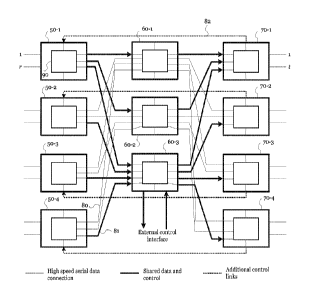
Figure 3 shows an example of how this might be achieved for a three stage
processor
according to an embodiment of the present invention, of the type shown in
Figure 2,
comprising four input Modules 50-1, 50-2, 50-3, 50-4 (R = 4), three
intermediate
modules 60-1, 60-2, 60-3 forming an intermediate stage (S = 3) and four output
modules 70-1, 70-2, 70-3, 70-4 (T = 4). Data flow between the modules is
configured by
a suitable design of cable harness to be unidirectional from input to output
with at least
one connection from each module in one stage to each module in the next.
io High speed serial data connections 8o between modules are shown in
Figure 3, but in
this example it is possible to provide a large proportion of the control
connectivity
required to access all of the modules via an external control interface by
making use of
existing data connections 81, shown in Figure 3 using thicker lines,
representing shared
data/control links. One of the modules is connected to the external control
interface for
telecommand or telemetry. Since each module is equipped with an external
control
interface, this could be any of the modules but one of the intermediate (also
referred to
hereinafter as a "middle") rank modules 60-3 is shown as connected to the
control
interface in Figure 3. The term "rank" groups modules which are the same
logical
distance, in terms of the number of other modules included in a signal path,
from an
input and/or output. Such sub-groups, [50-i, 50-2, 50-3], [60-1, 60-2, 60-3],
[70-1, 70-
2, 70-3] may be associated with a particular processing function, for example,
as
described below.
Control network routers 90 in each module allow control messages to be passed
around
the subset of active connections forming the control network. In the example
shown, it
is not possible to get two-way communication between all modules without
adding
some additional connections solely for control and synchronisation messages
because
the data flow for the interconnections is unidirectional. A possible
arrangement for
these extra control connections is depicted via dotted lines 82 in Figure 3.
With a
relatively small number of additional cables it is thus possible to form
looped control
paths allowing both read and write access to every module via the external
control
interface. For redundancy purposes it would be normal to supply spare external
control
interfaces and provide additional spare cabling to ensure reliable operation
even after
the failure of one or more modules.
CA 02957486 2017-02-07
WO 2016/034883 PCT/GB2015/052547
- 13 -
It should be noted that many possible topologies can be implemented and the
control
network can be implemented "internally" via shared data interconnections,
"externally"
via a network using the standard control interfaces on each module, or by a
mixture of
both. It should also be noted that provision for high speed digital
interconnections on
all module types, including input and output modules, includes quantities of
both input
and output connections. Thus the connectivity between modules is not
restricted to be
unidirectional and two-way connections can also be used to simplify the
control
network when desired.
/o The high degree of independence between modules and a common interface
standard
allow the accommodation of almost arbitrary configurations on board a
spacecraft. As
described above, each module is mechanically, thermally and electrically
independent
and also self-sufficient in terms of control functions. The modules can thus
be regarded
as "standalone" modules. This degree of isolation is made possible by the use
of high
/5 speed serial cable interconnections between modules, which enables a
potentially high
number of modules to be used without excessive cabling, suitable, for example,
for a
high capacity digital channelizer. Of course, variants of this architecture
are possible in
which modules are grouped, trading off flexibility for some other advantage.
For
example it is possible to share one power supply between multiple modules to
obtain an
20 efficiency saving in mass or power. It is also possible to group modules
mechanically,
for example by affixing numbers of them to a common baseplate before mounting
them
within the payload. These modifications of the described embodiments are
considered
to fall within the scope of the invention.
25 To implement a scalable digital channelizer and router using these
modules, for
example, it is necessary to include at least a minimum set of functions on
each of the
input, digital and output modules as shown in Figure 5, although the
particular
functions included will depend on the overall system to be constructed using
the
architecture of the present invention. To enhance understanding of the
operation of a
30 channelizer, in the context of which the subsequent embodiments are
described, the
functions of a channelizer are shown in Figure 4.
In order to be processed digitally, radio frequency input signals are first
filtered and
down-converted in frequency to provide a band-limited signal suitable for
analogue-to-
35 digital conversion. Each signal corresponds to a relatively wide
frequency band
segment from an uplink beam (or antenna feed, in the case of an active receive
CA 02957486 2017-02-07
WO 2016/034883 PCT/GB2015/052547
- 14 -
antenna) and generally contains frequency multiplexes consisting of numerous
carriers.
Each input, after digitization by an A/D converter, is then divided into
multiple
narrowband channels by a digital channel demultiplexer. Channels may then be
individually processed, typically including at least a gain control function,
and routed to
their destination downlink beams. Since the number of input and output beams
is
usually high, this routing function must be distributed across a network of
switching
components within the digital processor. On the output side, all of the
channels
destined for the same downlink beam are combined by a channel multiplexer to
form a
wideband signal which is then digital-to-analogue converted. Post-processing
io (frequency up-conversion and filtering) is then typically required to
generate a suitable
radio frequency signal for downlink transmission. Additional processing can
also be
added to the channelizer to increase the benefits of the digital processor,
such as power
monitoring, amplitude and phase weighting for digital beam-forming,
compensation
for gain non-flatness and group delay variations. Additional stages for
demodulation,
decoding, re-encoding and modulation can also be added to build a regenerative
on-
board processor as set out in more detail below. The outer layers of channel
processing
are used to separate the individual carriers for regeneration and to recombine
them to
form suitable outputs and in general still conform to the architecture shown
in Figure 1.
In the architecture of the present invention, the input modules implement the
front end
processing, including channelization and a first stage of switching for
transparent
routing. The number R of such modules is selected according to the total
number of
inputs required for a particular mission. Figure 5 illustrates a
representative input
module wo, containing a number of channel demultiplexers 101 in each of the
input
paths. The channel outputs from the r demultiplexers in general require a
first stage of
switching within the module 100 to support flexible end-to-end channel
routing,
performed by switch 102. Other functions, such as gain control, A/D conversion
and
additional analogue pre-processing may also be included within each input
module
loft High speed digital serial interface logic 103 is illustrated in each
signal path
following the switch, which may include input as well as output interfaces to
support
general signal flow topologies. Overall control of the input module wo is
performed by
a control module 104, powered by power supply io5. The control module and
power
supply render the input module self-sufficient as a standalone module.
Output processing consists of essentially the reverse process, performed by a
number T
of output modules for back end signal processing, each with internal switching
for
CA 02957486 2017-02-07
WO 2016/034883 PCT/GB2015/052547
- 15 -
transparent routing and channel multiplexers to recombine channelized
frequency
bands to generate t output signals suitable for downlink transmission. Again,
further
functions such as gain control, D/A conversion and additional post-processing
may be
included within each output module in alternative embodiments of the present
invention. Figure 5 illustrates a representative output module 120 containing
high
speed digital serial interface logic 123, a switch 122, channel multiplexers
121, control
124 and a power supply 125. As with the input module loo, the output module
120 can
operate as a standalone module.
io Routing is implemented with S intermediate modules, linked to a control
mechanism.
Representative intermediate modules no are shown in Figure 5, containing high
speed
serial digital interface logic for inputs (1n) and outputs (113). Routing is
performed
using switch 112. Power is provided from power supply 115, and control is
performed by
the control module 114.
Interconnection between all of the inputs and outputs is provided with the aid
of
intermediate modules to implement, as a minimum, switching between channelized
data carried between numbers of input and output high speed digital
interconnections.
The digital links require serialisation/deserialisation (SERDES) logic 103,
111, 113, 123.
The switching modules are typically arranged into ranks but this is not a
requirement
and any topology can be used for interconnections including loops if so
desired. The
switching modules can also be reprogrammable and be augmented by including
general-purpose processing elements in some embodiments, for additional
filtering or
signal monitoring, for example.
Examples are shown in Figure 6 with one intermediate rank 141 of cross-
connected
intermediate modules 141-1...141-S for switching, suitable for moderate scale
missions,
shown in Figure 6(b), with input modules 140-1...140-R each having r inputs
and
output modules 144-1...144-T each having t outputs connected to the
intermediate rank
via cable harnesses 145. Three intermediate ranks 151, 152, 153 are shown in
Figure
6(c), suitable for large scale missions, where input modules 150-1...150-R and
output
modules 154-1...154-T are connected via cable harnesses 155 to a first rank of
intermediate modules 151-1...151-Si, a second rank of intermediate modules
1.52-1...1.52-
S2 and a third rank of intermediate modules 153-1...153-S3. The number of
ranks may be
extended arbitrarily until the limits of payload accommodation are reached.
The case of
zero intermediate switching ranks is also admissible as shown in Figure 6(a),
were only
CA 02957486 2017-02-07
WO 2016/034883 PCT/GB2015/052547
- 16 -
input modules 130-1...13o-R and output modules 134-1..134-T are shown,
connected via
cable harness 135, and this arrangement is suitable for small scale missions
using the
switching capacity intrinsic to input and output modules. In the arrangements
of Figure
6, the input modules perform channel demultiplexing and switching, based on
input
module wo of Figure 5, the intermediate modules perform routing, based on
intermediate module no of Figure 5, and the output modules perform channel
multiplexing and switching, based on the output module 120 of Figure 5.
The numbers of each module type can be tailored freely to suit any digital
channelizer
/o mission size in step sizes of r inputs and t outputs. The values of r
and t are fixed in the
module designs with sufficiently small values that it is possible to get very
close to any
scale requirement with little inefficiency in terms of unnecessary hardware.
The
number of switching intermediate modules can be varied according to the
capacity
required and the flexibility of routing. The number of module interconnections
can also
/5 be varied by adding or removing cable connections within the switch
network formed
by the intermediate modules. Additional connections within a switch network
can
improve flexibility, for example, by reducing the number of rearrangements
needed
during operation to accommodate additional traffic channels or to support more
multi-
cast traffic routing scenarios. Unnecessary cable connections can also be
removed,
20 allowing missions with less demanding requirements to take benefit in
reduced mass
and power.
The principle advantage of this solution is that any on-board digital
channelizer can be
implemented using three standardised module designs that can be reused with no
re-
25 design or re-qualification needed between missions of differing scale
other than the
cable harness. In contrast to solutions in which the overall processor is
partitioned into
end-to-end slices, embodiments of the present invention allow efficient
implementation
of systems with unequal numbers of inputs and outputs. This is desirable
because on-
board channelizers filter out unwanted signals, generating fewer outputs than
inputs,
30 or they multi-cast signals to several outputs, increasing the output
side capacity, or to
suit a variety of antenna, payload or system requirements. Additionally, the
implementation of the complex connectivity required for high capacity switch
networks
is much simpler using cables than printed circuit board technology. The three
dimensions available for cable routing provide plenty of scope to accommodate
even
35 the largest missions whereas the limited number of cross-overs that can
be achieved in
CA 02957486 2017-02-07
WO 2016/034883 PCT/GB2015/052547
- 17 -
two-dimensional printed circuit board technology, such as that used in back-
plane
solutions, may seriously constrain the routing flexibility for larger scale
processors.
The architecture of Figure 6(b), and its extensions to larger switch networks
comprising
more ranks, is compatible with a digital beam-forming solution in which one or
more
intermediate ranks of modules is used to perform either receive or transmit
narrowband digital beam-forming with each module handling a subset of
frequency
channels from all of the antenna feed signals. To implement this in the
present
invention it is only necessary to supplement the switch function on the
intermediate
/o module used in the digital channelizer with the amplitude and phase
weightings,
accumulations and rearrangements required for digital beam-forming. This can
be
done by augmentation, reprogramming or replacement of processing components on
the intermediate module without other alteration to the hardware. The
intermediate
module can therefore be extended to serve as a dual mode switch/beamformer
module.
It will be appreciated, however, that other extensions will be apparent on
reading the
present disclosure.
A specific example of use of the architecture of Figure 5, as an embodiment of
the
present invention, is shown in Figure 7 with r = t = 4, with the inclusion of
integral
power supplies 165, 175, 185 and control functions 164, 174, 184, a gain stage
166, 176,
186 in each module, A/D converters 161 and channel demultiplexers 162 in each
input
path of the input modules 160 and D/A converters 181 and channel multiplexers
182 in
each output path of the output modules 180. In the context of a channelizer,
the input
modules may be regarded as receive modules, the intermediate modules as
switching
modules, and the output modules and transmit modules. The input modules 160
comprise a switch 163, followed by SERDES logic 167 before the output of the
module,
while the output modules 180 comprise SERDES logic 187 at the module input,
followed by a switch 183. The intermediate modules 170 comprise SERDES logic
177,
178 either side of the routing switch 173.
Implementations of digital channelizing processors for use on board satellites
typically
use application-specific integrated circuits (ASICs) as the main processing
components
for their superior radiation hardness and power efficiency but the designs are
hardwired and their function cannot therefore be subsequently modified.
Alternatively,
reprogrammable components such as field programmable gate arrays (FPGAs),
microprocessors or programmable digital signal processing (DSP) chips can be
used.
CA 02957486 2017-02-07
WO 2016/034883 PCT/GB2015/052547
- 18 -
These components have relatively higher power dissipation for a given
processing
performance but can be re-programmed subsequently to manufacture.
The architecture of the present invention is not reliant on the choice of one
or other and
in fact can support either within the same physical module. This allows large
scale
processors to be implemented with maximum efficiency using ASIC components and
smaller processors to be implemented more rapidly using reprogrammable
components, and is a demonstration of the flexibility of the present
invention.
io Replacement of ASIC with reprogrammable components such as FPGAs may
require
modification of the internal design of the module but, since all of components
including
the power supply are internal to each module, as shown in Figure 7, for
example, the
external module interfaces remain identical. As a consequence, it is
straightforward to
support mixed architectures by implementing a subset of the modules using
reprogrammable components such as FPGAs. This can be used, for example, to
incorporate additional specialised processing functions into the middle of the
processing chain or to provide alternative channelizer characteristics in the
receive and
transmit modules.
An on-board signal processing application which benefits particularly from
reprogrammable technology is regenerative processing for satellite
telecommunications. Regeneration of the uplinked data involves demodulation of
individual carrier signals in the processor and the ability to update the on-
board
modem functions, and is desirable to keep pace with ground terminal evolution
over
the lifetime of the satellite. "Regenerative processing" refers to the fact
that original
information contained within a signal is "regenerated" and processed, in
contrast to
"transparent processing" which involves processing a particular signal without
the
processor having a knowledge of the information contained in the signal.
Channelization and routing functions similar to those of the digital
channelizer are
typically used at the front end of the digital processing chain to select and
isolate
specific carrier signals for demodulation. Figure 8 shows how all of the
functions
required of a typical end-to-end regenerative processor could be constructed
using the
architecture of the present invention by using reconfigurable logic versions
of the
intermediate modules 210 to implement the regenerative functions. The
intermediate
modules may comprise a first rank 211 of X modules for demodulation and
decoding, a
CA 02957486 2017-02-07
WO 2016/034883 PCT/GB2015/052547
- 19 -
second rank 212 of Y modules for packet routing, and a third rank 213 of Z
modules for
modulation and encoding. The R input 200 and T output 220 modules are reused
to
connect the front and end of each chain with as many intermediate modules as
required
in between to implement the regenerative functions. The input and output
modules can
be implemented using either fixed or reconfigurable logic as appropriate.
Since regenerative functions require much more processing than transparent
functions,
and are therefore expensive to implement on board, hybrid solutions performing
predominantly transparent processing with only a subset of traffic undergoing
io regenerative processing may be optimal. The architecture of the present
invention is
capable of supporting numerous variations of this type of architecture. Two
examples
are given in Figure 9, representing embodiments of the present invention. The
first,
shown in Figure 9(a), is the simplest, requiring just the replacement of one
or more
centre rank intermediate modules from the architecture of Figure 6(b) with the
reconfigurable version. This architecture could be used to implement a small
number of
modems on a single module. The connections to each receive and transmit module
allow the regenerated channels to be selected from any of the uplinks and
inserted on
any of the downlinks, making use of the routing functions within those
modules. The
embodiment of Figure 9(a) contains R input modules 230, S intermediate modules
240, a regenerative processor 250 in the intermediate rank, and T output
modules 260.
For larger systems with more flexible routing requirements, an architecture
such as the
one in Figure 9(b) could be used. Here a subset of the outputs of S middle
rank
intermediate modules 280 performing switching are connected to the inputs of a
regenerative processor 285, which may itself consist of multiple
reconfigurable versions
of the intermediate modules, and whence the outputs are fed back into spare
inputs on
the middle rank of intermediate modules. In this way two stages of switching
are
implemented before and after the regenerative processor, allowing more
flexible
handling of larger volumes of regenerated traffic. As with Figure 9(a), there
are R input
modules 270 and T output modules 290.
Although a number of embodiments have been described with respect to a digital
channelizer, this is simply an example of a system which can be constructed
using the
architecture of the present invention, and alternative systems may be
constructed via
appropriate configuration of input modules, output modules and intermediate
modules.
CA 02957486 2017-02-07
WO 2016/034883 PCT/GB2015/052547
-20 -
Methods of testing a digital signal processor formed according to the
architecture
described above in relation to previous embodiments also fall within the scope
of the
present invention. The division of the processing functions into physically
distinct
modules enables a phased testing process to be carried out before the full
scale
processor is tested. The phased testing may be applied to individual modules,
or to
groups of modules. If an error is identified in connection with any individual
module, it
is therefore much quicker to replace or reconfigure this module having
identified the
error on the basis of an individual test rather than through performing
diagnosis of the
io error through testing of the full scale processor, as would be required
in a "single box"
solution where the source of the error may be difficult to identify. The
advantages of the
use of the architecture of the invention are thus apparent.
Testing can be applied prior to use of the digital signal processor, but may
also be
/5 applied as a routine or scheduled process during use of the processor,
namely
operational testing. As a result of the test, redundancy can be exploited
through routing
signals through replacement modules where necessary.
Given the potential to use the architecture of the present invention for space-
based
20 applications, the testing which is performed may include environmental
testing as well
as functional testing, in order to determine whether the on-board processor
can
withstand the conditions to which it is likely to be exposed on a particular
mission, such
as severe vibration and acceleration, extremes of temperature, and subjection
to high
levels of radiation and electromagnetic interference, in orbit or during the
launch
25 phase. A phased approach to environmental testing can be particularly
valuable both to
allow an early retirement of the major risks associated with a test failure
and to allow
the use of smaller scale test facilities compared to testing a large-scale
integrated
processor.
30 It will be appreciated that a number of modifications to the embodiments
described
may be made which fall within the scope of the invention on account of using
the
architecture set out in the claims. Compatible features of different
embodiments may
be combined, as will be apparent to the skilled person, without loss of the
generality of
the underlying architecture. The scalability of the architecture which has
been
35 described can be achieved through appropriate selection of the number of
input,
intermediate and output modules, the number of ranks of intermediate modules,
and
CA 02957486 2017-02-07
WO 2016/034883 PCT/GB2015/052547
- 21 -
the number of intermediate modules within each rank. The fact that each module
is
"self-contained", or independent, and is typically small in size, connected
via high
speed cables, enables interchangeability, redundancy and scalability within a
particular
system, without requiring any modification of the module hardware designs,
leading to
the possibility of a wide range of applications both within and outside the
field of
telecommunications.