Note: Descriptions are shown in the official language in which they were submitted.
CA 02959059 2017-02-22
WO 2016/057125 PCT/US2015/046774
MICROCAVITY ARRAY FOR SPECTRAL IMAGING
FIELD
The disclosure pertains to spectral imaging.
CROSS-REFERENCE TO RELATED APPLICATIONS
This application claims the benefit of U.S. Provisional Application
62/041,529, filed August
25, 2014, which is incorporated herein by reference.
BACKGROUND
High resolution spectral imaging systems have numerous potential applications,
but typical
systems that provide adequate spectral and spatial resolution are often
impractical. Spectral
analysis can be obtained using diffraction gratings, optical filters, Fabry-
Perot interferometers, or
other optical systems. Conventional tunable filters such as described in Lin
et al., U.S. Patent
7,734,131 and Smith et al., U.S. Patent Publication 2015/0103343 require
complex, specialized
fabrication processes. For many applications, such conventional systems remain
impractical.
Systems based on diffraction gratings and optical filters can be
inconveniently large and tuning is
often slow. Conventional Fabry-Perot interferometer-based systems can be used
but conventional
Fabry-Perot interferometers are difficult to maintain in alignment and have
spectral resolutions that
are not suitable for many applications.
BRIEF SUMMARY OF THE INVENTION
The disclosure pertains to optical devices, methods, and systems for spectral
imaging and
other applications. According to some examples, optical devices include first
and second reflectors
and a liquid crystal layer situated between the first and second reflectors.
The liquid crystal layer
and the first and second reflectors define an optical cavity and first and
second conductive
electrodes are situated to define a plurality of electrically controllable
microcavities in the optical
cavity. In some examples, at least one of the first and second conductive
electrodes includes a
plurality of microcavity electrodes that define the electrically controllable
microcavities. In typical
examples, at least one of the first and second conductive electrodes is
situated external to the
optical cavity. In some embodiments, the optical devices include a first
transparent substrate,
wherein the first reflector is situated at a cavity-facing surface of the
first transparent substrate, and
a second transparent substrate, wherein the second reflector is situated at a
cavity-facing surface of
1
CA 02959059 2017-02-22
WO 2016/057125 PCT/US2015/046774
the second transparent substrate. In representative examples, the microcavity
electrodes are
arranged so as to form a microcavity electrode array, and the cavity-facing
surface of the first
substrate includes a plurality of concave portions, each concave portion
corresponding to a
respective microcavity. In some examples, the first and second reflectors are
dielectric reflectors
having reflectivities of at least 90% in a selected spectral range. According
to some embodiments,
the first conductive electrode includes a plurality of microcavity electrodes
that define the
electrically controllable microcavities. The optical devices further include a
plurality of transistors,
each of the plurality of transistors coupled to a respective microcavity
electrode. In some cases, a
microlens array is secured to a surface of the first substrate that is
opposite the cavity-facing surface,
wherein each lens of the microlens array is situated along an axis of a
respective microcavity.
Spectral imagers comprise a Fabry-Perot tunable filter having a plurality of
liquid crystal
tunable microcavities and an image sensor optically coupled to the Fabry-Perot
tunable filter.
Typically, the image sensor includes plurality of pixels, and the liquid
crystal tunable microcavities
are situated so as to be optically coupled to corresponding image sensor
pixels. In representative
examples, the Fabry-Perot tunable filter includes a substrate having a high
reflectance coating on a
microcavity-facing surface, and the substrate is secured to the image sensor.
In some cases, each
microcavity is optically coupled to different image sensor pixels. According
to further examples,
the Fabry-Perot tunable filter includes an array of tunable microcavities and
the image sensor
includes an array of pixels. In some embodiments, the Fabry-Perot tunable
filter includes first and
second substrates having high reflectivity coatings on respective microcavity-
facing surfaces and a
liquid crystal layer is situated between the first and second substrates,and
the image sensor includes
an image sensor window, further wherein one of the first and second substrates
is fixed to the
image sensor window.
Methods of making a spectral imager comprise defining an array of LC
microcavities and
securing the array of LC microcavities to an image sensor array so that LC
microcavities are
optically coupled to respective sensors of the image sensor array. In some
examples, the array of
LC microcavities is defined by forming a first reflective coating in a
selected spectral region on a
first substrate; forming a second reflective coating in the selected spectral
region on a second
substrate; and situating an LC layer between the first and second reflective
coatings. In further
examples, the array of LC microcavities is situated between a first conductive
coating and a second
conductive coating, wherein at least one of the first conductive coating and
the second conductive
coating is patterned so as to define the LC microcavities. In other examples,
an array of regions in
a surface of the first substrate is ablated, wherein the first reflective
coating is formed on the array
of ablated regions. In still further examples, a microlens array is secured
with respect to the array
2
CA 02959059 2017-02-22
WO 2016/057125 PCT/US2015/046774
of LC microcavities so that the microlenses are situated to direct input
optical radiation to
associated LC microcavities and corresponding image sensor pixels.
In a representative example, spectral imagers comprise a tunable filter
defined by a liquid
crystal layer situated between first and second transparent substrates, the
first transparent substrate
having an array of surface depressions and a dielectric coating at the surface
depressions, the
second substrate having a dielectric coating, wherein the dielectric coatings
of the first and second
substrates and the array of depressions define an array of liquid crystal
Fabry-Perot cavities. An
image array is secured to the tunable filter, so that the liquid crystal Fabry-
Perot cavities are
optically coupled to corresponding photodetectors of the image array. A
piezoelectric device is
coupled to at least one of the first and second substrates so as to adjust a
spacing of the liquid
crystal Fabry-Perot cavities. A liquid crystal driver and a piezoelectric
driver are coupled to the
tunable filter so as to select a plurality of wavelengths for each of the
liquid crystal Fabry-Perot
cavities, and a processor receives images from the image array and provides a
spectral data cube
based on the images.
BRIEF DESCRIPTION OF THE DRAWINGS
FIG. 1 is a schematic sectional diagram of a representative Fabry-Perot
tunable filter that
includes a plurality of microcavities.
FIG. 2 illustrates a portion of an active matrix addressed liquid crystal (LC)
array for a
Fabry-Perot tunable filter.
FIGS. 3A-3B illustrate a representative method of tuning microcavities of a
Fabry-Perot
tunable filter in which selected microcavities are tuned to different
wavelengths.
FIGS. 4A-4B illustrate a representative method of tuning microcavities of a
Fabry-Perot
tunable filter in which each row of microcavities is tuned to a common
wavelength.
FIG. 5 illustrates a spectral imaging system that includes a Fabry-Perot
tunable filter and an
array image sensor.
FIG. 6 illustrates a representative arrangement of image sensor elements and
LC
microcavities.
FIG. 7 illustrates a method of obtaining a spectral image.
FIG. 8 illustrates a method of fabricating a Fabry-Perot (FP) tunable filter.
' FIG. 9 illustrates spectral transmission of a tunable FP filter,
indicating a spectral bandwidth
associated with selection of a wavelength range within a selected free
spectral range (FSR).
FIG. 10 illustrates spectral tuning offsets associated with microcavity
fabrication variations.
FIG. 11 illustrates a representative spectral imager based on a tunable LC FP
array.
3
CA 02959059 2017-02-22
WO 2016/057125 PCT/US2015/046774
FIG. 12 illustrates a spectral imager in which a tunable FP array is imaged
onto an array
detector.
DETAILED DESCRIPTION
As used in this application and in the claims, the singular forms "a," "an,"
and "the" include
the plural forms unless the context clearly dictates otherwise. Additionally,
the term "includes"
means "comprises." Further, the term "coupled" does not exclude the presence
of intermediate
elements between the coupled items.
The systems, apparatus, and methods described herein should not be construed
as limiting in
any way. Instead, the present disclosure is directed toward all novel and non-
obvious features and
aspects of the various disclosed embodiments, alone and in various
combinations and sub-
combinations with one another. The disclosed systems, methods, and apparatus
are not limited to
any specific aspect or feature or combinations thereof, nor do the disclosed
systems, methods, and
apparatus require that any one or more specific advantages be present or
problems be solved. Any
theories of operation are to facilitate explanation, but the disclosed
systems, methods, and apparatus
are not limited to such theories of operation.
Although the operations of some of the disclosed methods are described in a
particular,
sequential order for convenient presentation, it should be understood that
this manner of description
encompasses rearrangement, unless a particular ordering is required by
specific language set forth
below. For example, operations described sequentially may in some cases be
rearranged or
performed concurrently. Moreover, for the sake of simplicity, the attached
figures may not show
the various ways in which the disclosed systems, methods, and apparatus can be
used in
conjunction with other systems, methods, and apparatus. Additionally, the
description sometimes
uses terms like "produce" and "provide" to describe the disclosed methods.
These terms are high-
level abstractions of the actual operations that are performed. The actual
operations that correspond
to these terms will vary depending on the particular implementation and are
readily discernible by
one of ordinary skill in the art.
In some examples, values, procedures, or apparatus' are referred to as
"lowest", "best",
"minimum," or the like. It will be appreciated that such descriptions are
intended to indicate that a
selection among many used functional alternatives can be made, and such
selections need not be
better, smaller, or otherwise preferable to other selections.
Examples are described with reference to directions indicated as "above,"
"below," "upper,"
"lower," and the like. These terms are used for convenient description, but do
not imply any
particular spatial orientation.
4
CA 02959059 2017-02-22
WO 2016/057125 PCT/US2015/046774
As used herein, "optical radiation" refers to propagating electromagnetic
radiation at
wavelengths between about 100 nm and 10 p m, typically between 400 nm and 2 p
m. Optical
radiation is generally referred to as propagating in optical beams. As used
herein, an "image"
refers to a spatial distribution of optical intensity, typically a one or two
dimensional distribution or
an analog or digital representation of such a distribution, including stored
representations in a
computer readable medium or device such as RAM, ROM, or a hard disk. As used
herein,
"spectral image" refers to a spectrally resolved optical intensity
distribution, or an analog or digital
representation of a spectrally resolved optical intensity distribution stored
in a computer readable
medium or device such as RAM, ROM, or a hard disk. In some examples, a Fabry-
Perot tunable
filter is scanned over a selected wavelength range, and a series of spectral
images is acquired and a
spectral data cube is obtained having optical intensity as a function of
wavelength and two-
dimensional position. In some examples, lenses or microlenses are provided,
but in other examples,
mirrors, holographic optics, or other reflective or refractive optical devices
can be used.
Fabry-Perot (FP) based tunable filters as disclosed herein generally include
first and second
reflectors situated about a liquid crystal (LC) material having an index of
refraction that varies in
response to an applied electric field. The first and second reflectors and the
liquid crystal material
generally establish an optical resonant cavity, referred to simply as an
optical cavity herein. Such
an optical cavity can be divided into a plurality of independently
electrically tunable portions
referred to as microfilters or microcavities. Typically, such microcavities
have transverse
dimensions less than a few mm, but the term "micro" is not intended to require
a particular size or
size range. In most examples, both reflectors are defined on respective
substrates, and at least one
of these substrates is transparent in a spectral range of interest so that
optical radiation can be
coupled into the optical cavity and optical microcavities. Surfaces of
substrates that are closest to a
Fabry-Perot cavity are referred to herein as cavity-facing. For transmissive
FP tunable filters, both
first and second substrates are transparent, while for reflective FP tunable
filters, one of the first
and second substrates is transparent and the other is reflective. As used
herein, a transparent
substrate is a substrate having an internal transmittance of greater than 10%,
25%, 50%, 75%, or
90% in a selected spectral range. In some cases, overall substrate
transmittance can be improved
with antireflection coatings.
Electrically variable optical path length is provided with one or more liquid
crystal layers.
Electrical signals (typically voltages) applied to a liquid crystal layer
produce optical path length
changes based on orientation changes in the liquid crystal layer. Alignment in
liquid crystal layers
is generally provided with alignment layers on opposing surfaces that contain
the liquid crystal.
Alignment layers can formed as rubbed polyimide layers or other layers can be
used. Liquid crystal
CA 02959059 2017-02-22
WO 2016/057125 PCT/US2015/046774
optical path differences and switching speed are typically functions of a LC
layer thickness that can
be established using perimeter spacers, spacers situated on portions of
substrate surfaces that
contain the LC layer, or with spacers distributed within the LC layer. For
convenient illustration,
such alignment layers and spacers are not shown in the accompanying drawings.
In typical
implementations, nematic liquid crystals are used.
Portions of a liquid crystal can be individually addressed so as to permit
independent tuning
of microcavities. Such LC portions are sometimes referred to as "pixels," as
similar independently
tunable portions serve as picture elements in LC displays. LC addressing in
the disclosed tunable
filters can be based on so-called direct addressing in which row and column
electrodes are situated
on opposing sides of an LC layer. In other examples, so-called active matrix
addressing is used in
which row and column electrodes are situated on a common substrate and coupled
via a transistor
implemented as a thin film transistor (TFT) so as to regulate an applied
voltage. An additional
electrode is situated on an opposing side of the LC layer, but patterning of
this additional electrode
is not required for individual pixel control, although can be provided for
other reasons, if desired.
Tunable optical path lengths in LC layers often depend on a state of
polarization (SOP) of
optical radiation directed into the LC layers. In some cases, one or more
polarizers (and retarders)
is situated to select a suitable SOP. Such polarizers can generally be
situated to select a SOP prior
to transmission through the LC layer or after transmission through the LC
layer.
In some examples, CMOS image sensors (CIS) are used. Typical CIS devices
include an
array of light sensitive areas (pixels) and circuitry that scans each pixel at
fixed intervals to produce
an electrical signal corresponding to optical intensity at the pixels. This
electrical signal is digitized
to produce a digital representation of the optical intensity distribution that
can be stored in a
computer-readable medium. Other types of image sensors such as charge coupled
devices,
photodiode arrays, or sets of discrete optical detectors such as photodiodes,
photovoltaic devices, or
other types of optical detectors can be used. Discrete devices can be mounted
and fixed in a regular
array, if needed. In most applications, two dimensional arrays are preferred,
but one dimensional
arrays can be used.
For convenience, certain terms used associated with FP devices are described.
Free spectral
2 2
range (FSR) is a spectral width between adjacent FP cavity resonances. FSR "=
at normal
2nL
incidence, wherein n and L are cavity refractive index and cavity length,
respectively, and 20 is a
free space optical wavelength. FSR varies as 1/cos(0) wherein 0 is an angle of
incidence.
6
CA 02959059 2017-02-22
WO 2016/057125 PCT/US2015/046774
Similar expressions can be obtained for cavities that comprise multiple layers
of different
z(RR)1/4
materials. FP cavity finesse is about F = 1 2 , wherein the FP cavity
is terminated by
1¨ (Rik )1/2
mirrors of reflectivity Ri and R2. In the disclosed examples, F can be as much
as 100, 200, or 500.
FP resolution is generally defined as FSRIF. Reflective coatings used to
define a FP cavity can be
patterned or unpatterned as may be convenient. While LC tunable FP cavity
length is based
primarily on reflector separation and LC layer thickness, penetration of
optical radiation into
reflective coatings can also contribute to cavity length (and vary FSR). In
some cases, such
variation is wavelength dependent and an LC cavity can be calibrated to
accommodate such
variability.
The disclosed systems and devices can be rugged and compact, and can provide
rapid
spectral imaging and many applications are possible. Typical applications
include pharmaceutical
and medical applications, such as skin cancer detection and, pharmaceutical
counterfeit detection.
Other applications include atmospheric sensing.
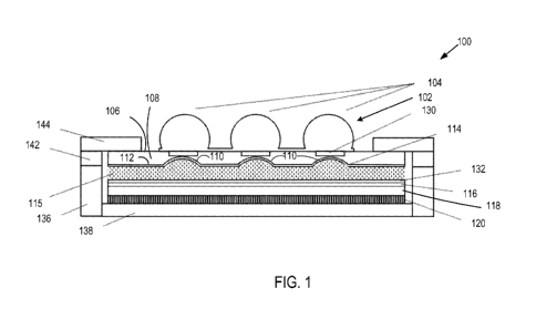
With reference to FIG. 1, a representative FP tunable filter 100 includes a
microlens array
102 that includes a plurality of microlenses 104 that can be secured to a
first surface 106 of a
substrate 108 or integrally formed in the substrate 108. Alternatively, the
microlens array 102 can
be situated proximate the substrate 108 so that a position of the microlens
array 102 can be adjusted
with respect to individual FP microcavities as described in detail below. A
plurality of curved
surface portions 110 are also formed on a second surface 112 of the substrate
108, and a first
dielectric coating 114 is provided on the second surface 112, either on the
entire second surface 112
or at the curved surface portions 110. As shown in FIG. 1, the curved surface
portions 110
correspond to depressions in the second surface 112. Typically, the curved
surface portions 110 are
arranged in a regular array that corresponds to the arrangement of the
microlenses 102.
A liquid crystal layer 115 is situated between the first dielectric coating
114 and a second
dielectric coating 116 that is situated on a second substrate 118, such as a
silicon substrate or other
substrate that is suitably transmissive in a spectral region of interest. The
second substrate 118 can
be secured to a CCD image sensor 120 (or other image sensor) or can be spaced
apart from the
CCD image sensor 120 with an additional transparent substrate. In some
examples, the second
substrate 118 is glued to an image sensor window or cover plate with an
optical adhesive.
Conductive electrodes 130, typically formed of a transparent conducive
material such as indium tin
oxide, are provided at the first surface 106 of the first substrate 108.
Alternatively, the conductive
electrodes 130 can be situated between the dielectric coating 114 and the
second surface 112 or
other convenient location. An additional conductive layer 132 can be situated
between the second
7
CA 02959059 2017-02-22
WO 2016/057125 PCT/US2015/046774
substrate 118 and the second dielectric coating 116 or on a cavity-facing
surface of the second
dielectric coating 118.
The image sensor 120 includes an array of photodetectors or photosensitive
regions,
referred to herein as pixels, and the microlenses 104 are aligned so as to be
approximately centered
with respect to corresponding image sensor pixels or sets of such pixels. The
FP tunable filter 100
can be secured to or retained by a housing that comprises housing portions
136, 138. A
piezoelectric device 142 is coupled to the first substrate 106 via a housing
portion 144 to permit
adjustment of a separation between the first dielectric coating 114 and the
second dielectric coating
116 as well as to align the microlenses 130.
The first dielectric coating 114 and the second dielectric coating 116 are
generally highly
reflective in a wavelength range of interest and serve to define a Fabry-Perot
cavity having an
optical path length that is variable in response to displacements introduced
with the piezoelectric
device 142 and orientation or other electro-optical property of the liquid
crystal layer 115. The
Fabry-Perot tunable filter of FIG. 1 uses a planar reflector (the second
dielectric coating 116) and
concave reflectors (dielectric coated surface portions 110). One or more
curved reflective surfaces
can increase fabrication tolerances and provide improved Fabry-Perot finesse,
and cavities can be
symmetric or asymmetric. Curved or planar reflective surfaces can be used for
one or both
reflective surfaces. Conductive coatings are preferably situated external to
the FP optical cavity,
i.e., not between the first and second dielectric coatings 114, 116 so that
any associated losses are
external to the FP cavity, and do not reduce finesse.
The piezoelectric device 142 can adjust a spacing of the first substrate 108
and the second
substrate 118 so as to adjust cavity length of all microcavities. The LC layer
can be used to adjust
cavity length (i.e., optical path length) based on voltages applied to the
conductive electrodes 130,
132.
The curved surface portions 110 can be formed by laser ablation using optical
pulses from a
CO2 laser (10.6 p m) or at another wavelength that is absorbed by a selected
substrate material.
Representative materials include glass and fused silica. In one example, a CO2
laser beam is
focused to a 20 p m (1/e2) spot on a fused silica substrate surface with a
pulse duration of between
p s and 100 p s with an axial fluence of about 25 J/cm2 (pulse energy of about
3 mJ). Laser beam
quality corresponding to M2 < 1.2 is preferred. Surface depressions of
diameters less than 50 p m,
depths less than 800 nm, and radius less than 800 p m can be produced. A
series of such exposures
is used to produce an array of curved surface portions as shown in FIG. 1.
Center-to-center
spacings of 10 p m to 20 p m can be produced to match liquid crystal and image
sensor array
dimensions. After curved surface portions are produced, a dielectric coating
is applied to serve as a
8
CA 02959059 2017-02-22
WO 2016/057125 PCT/US2015/046774
cavity end min-or. Smooth surfaces (rms roughness <0.34 nm) can be produced so
that high
reflectivity dielectric coatings can be successfully applied. Depths are
somewhat variable, but
liquid crystal tuning can be used to correct for depth variations among the
ablated areas.
A liquid crystal layer thickness can be selected based on a desired free
spectral range and
resolution, and achievable values of finesse. Liquid crystal layers are
generally selected to tune
over a full free spectral range. LC tunable refractive index differences can
be as large as 0.3 so a 1/2
wave phase difference at most wavelengths of interest can be produced with LC
layer thickness of a
few microns. Typical thicknesses range from about 1 p m to about 100 p m, 1 p
m to about 50 p m,
1 p m to about 20 p m, or 1 p m to about 10 p m.
With reference to FIG. 2, a representative active matrix addressed, tunable LC
array 200 for
use in a Fabry-Perot tunable filter includes a plurality of LC regions (for
example, region 202) that
are situated at or near intersection of signal lines (a-x) and perpendicular
gate lines. The LC array
200 is coupled to support members 204, 205 so that the LC array 200 can be
aligned with microlens
arrays and/or an image sensor. Each of the LC regions is associated with a
conductive ITO
electrode and a transistor. For example, a representative LC region 232 is
associated with a
conductive electrode 206 and a transistor 208 that is coupled to a signal line
and a gate line.
Voltages applied to the signal and gate lines thus permit control of a voltage
on the electrode 206,
permitting control of an associated LC region. (An additional conductive
electrode on an opposing
side of the associated LC layer is not shown.) With the arrangement of FIG. 2,
each of the LC
regions can be individually tuned using suitable voltages applied to the
associated transistors. Thus,
each FP microcavity can be tuned substantially independently of others.
A representative method of driving an FP tunable filter array is illustrated
in FIGS. 3A-3B.
A plurality of FP microcavities A-I are driven so that each provides a maximum
transmission at a
different respective wavelength. In this example, each FP microcavity of an
array is tuned to a
different wavelength as shown in FIG. 3B. Another representative method of
driving a tunable FP
array is illustrated in FIGS. 4A-4B. Microcavity rows 402, 404, 406 are tuned
to respective
common wavelengths A-C having transmittances as shown in FIG. 4B. Other
groupings can be
tuned in common, such as rows, or other two-dimensional portions of an array
of microcavities.
The tunings A-C can be correspond to sequential wavelengths sequential and LC
microcavity rows
sequentially tuned over a desired range. For example, an array with n rows
could be tuned so that
each row is offset from an adjacent row about FSR/n or by 1/n of some other
scan range.
Alternatively, adjacent rows could be tuned to wavelengths separated by
microcavity resolution,
with or without scanning.
9
CA 02959059 2017-02-22
WO 2016/057125 PCT/US2015/046774
Referring to FIG. 5, a representative FP tunable filter system 500 includes an
optical system
502 that produces an image of a region of interest that is directed through a
free spectral range
(FSR) filter 504 or other filter to a FP liquid crystal tunable filter array
506. The FP array 506 is
coupled to a piezoelectric drive 508 that provides a suitable voltage or range
of voltages to a
piezoelectric device 510 that can adjust a FP cavity length. In some examples,
piezoelectric
elements are not used, or can be used for scanning in conjunction with or in
addition to liquid
crystal based scanning, or the piezoelectric device 510 can be used to set a
particular cavity length
and scanning provided with a liquid crystal element.
The FP array 506 is also coupled to a liquid crystal driver 512 that provides
suitable
electrical signals to microcavities of the FP array 506 so as to vary or
establish cavity lengths for
some or all microcavities of the FP array 506. In some examples, the liquid
crystal driver 512 can
be provided as a liquid crystal display driver so that wavelength tunings
settings such as scan range,
drive levels for some or all wavelengths, bias drive levels to establish a
selected initial or other
wavelength can be coupled to some or all microcavities. Alternatively the
liquid crystal driver 512
can be provided with dedicated circuit elements that can provide drive signals
similar to those
provided with display drivers, or larger, smaller, faster, or slower drive
signals as preferred. As
shown in FIG. 5, drive levels are based on tuning wavelength and calibration
settings that can be
stored and recalled from a memory 514, and are provided to the LC driver 512
so as to correspond
to image display values. A spectral tuner 515 select piezoelectric drive
levels, processes LC drive
values, and is coupled to a temperature controller 516. A temperature control
element (such as a
temperature sensor and/or thermoelectric device) 518 is coupled to the
temperature controller to
establish a temperature of the FP array 506. FP array temperature can be
selected to provide
selected FP microcavity lengths, to maintain consistent FP array spectral
properties in the presence
of external temperature changes, or to control or adjust LC switching speeds.
An imaging system 522 includes a detector array 524, a detector
amplifier/buffer 526, and
an analog-to-digital convertor (AID) 528. The detector array 524 is typically
a CCD or CMOS
array that includes a two dimensional array of photosensors such as
photodiodes. The detector
amplifier/buffer 526 and the AID 528 process signals from the photosensors
corresponding to a
local input optical intensity to produce image signals or image data that is
coupled to a memory 530
for storage. As noted above, one or two dimensional detector arrays can be
used, and a series of
spectral images can be obtained and the associated spectral datacube stored in
the memory 530. In
some examples, the imaging system 522 is implemented as a series of discrete
components similar
to the arrangement of FIG. 5, but other arrangements integrated image
sensors/processing
electronics can be used. In some examples, an image processor 534 receives
tuned images and
CA 02959059 2017-02-22
WO 2016/057125 PCT/US2015/046774
combines images based on wavelength tuning patterns (such as shown in FIGS. 4A-
4B-5A-5B) to
produce a spectral datacube.
The FSR 504 is selected to transmit spectral portions of the input image so as
to reduce or
eliminate optical power that reaches a detector that is outside of a selected
spectral window of
interest. Typically, the FSR 504 transmits optical power at wavelengths that
are within a range that
is less than or equal to one free spectral range. In this case, the periodic
transmission of the FP
array does not result in optical intensity at multiple FP resonance
wavelengths reaching the detector
array 524. The pre-filter can be a multilayer coated band pass filter having
pass band that is less
than a free spectral range, or a series of dielectric edge filters, or one or
more absorptive filters can
be used. Other spectrally selective optical elements such as diffraction
gratings, holographic
optical elements, or reflective filters can also be used. The FSR filter can
be situated optically
before or after the FP microcavity array.
While in some examples, LC microcavities are arrange to align with
corresponding image
detector pixels, other arrangements can be used. For example, as shown in FIG.
6, an array 600 of
image pixels is situated so that optical radiation from an LC microcavity 640
is directed to image
sensor elements 602, 603, 612, 613. Alternatively, a single LC microcavity can
be situated to direct
filtered optical radiation to image sensor elements arranged in a column such
as image sensor
elements 603, 613, 623 or image sensor elements arranged in a row such as
image sensor elements
622, 623, 624. Different FSR selecting filters can be applied to each of the
multiple image sensor
elements associated with a single LC microcavity to extend a spectral analysis
range to more than
one FSR. For example, as shown in FIG. 9, an Nth FSR and an (N+1)th FSR
corresponding to
different wavelength ranges can be assigned to different image sensor
elements, and scanned
simultaneously. In other examples, a single image sensor element can be
situated to receive filtered
optical radiation from multiple LC microcavities.
Referring to FIG. 7, a method 700 of obtaining spectral images includes tuning
a plurality of
FP cavities (typically, LC microcavities) at 702 and acquiring a spectral
image at 704. At 706, it is
determined if additional tunings are to be used. If so, 702, 704 are repeated
with a different tuning.
If spectral images associated with all selected tunings have been acquired,
images from the multiple
spectral tunings are combined as 708 and a combined spectral image or portions
thereof are stored
at 710. As noted above, all LC microcavities of an array can be tuned to a
common wavelength,
and scanned by scanning the common wavelength. However, some or all LC
microcavities can be
tuned to different wavelengths, so that a particular spectral image from a
single tuning contain
spectral data for different wavelengths at different image pixels. Using a
table of tunings, such
spectral images can be combined to produce, for example, a spectral datacube.
11
CA 02959059 2017-02-22
WO 2016/057125 PCT/US2015/046774
A method 800 of making a spectral imager includes forming an array of tunable
FP filters at
802 and aligning the tunable FP filters with an image sensor pixel array at
804. Typically, the array
of tunable FP filters is based on an array of LC tunable FP microcavities. At
806, the image sensor
is secured to the array of tunable FP filters.
FIG. 9 illustrates the periodically varying transmittance associated with an
FP tunable filter.
For a fixed tuning, optical radiation at a plurality of wavelengths can be
transmitted. By providing
an optical filter (referred to herein as an FSR selector or FSR filter) having
a passband
corresponding to an Nth FSR, radiation in other FSRs can be rejected. If an
FSR is sufficiently
large so that all input optical radiation spans a wavelength range that is
less than one FSR, such
filtering is generally unnecessary. In some cases, FP reflectors are
sufficiently narrowband so that
cavity resonance extends over a small spectral window, and additional
filtering is avoided.
As shown in FIG. 10, LC microcavities can have slightly different cavity
lengths or other
characteristics so as to tune differently with common tuning voltages. For
example, spectral curves
1002, 1004 correspond to different LC microcavities, nominally tuned to a
common wavelength.
The LC microcavities can be calibrated by tuning to a common wavelength, and
the associated
tuning parameters (such as LC drive voltage, piezoelectric drive voltage,
temperature) selected so
an array can be set to a common wavelength using the stored values.
A representative FP tunable filter array 1100 is shown in FIG. 11. A first
transparent
substrate 1102 includes a conductive coating 1110 and a reflective coating
1112. A second
substrate 1104 includes a conductive coating 1118 and a reflective coating
1116. An LC layer 1114
is situated between the substrates 1102, 1104. The substrate 1104 is secured
to a window 1122 of a
CCD image sensor 1106 with a layer 1120 of an optical adhesive. The conductive
coatings 1110,
1118 can be patterned for active or passive LC addressing, and the LC assembly
can be fixed to the
CCD image sensor 1106 with a housing, a mechanical assembly, or otherwise. If
needed, a
polarizer 1130 can be secured to the first substrate 1102. Alignment layers,
microlenses, additional
filters, and electrical connections and patterning of conductive layers are
not shown for convenient
illustration. As shown in FIG. 11, two planar reflectors can be used, and
microlenses and substrate
surface depressions are not required.
FIG. 12 illustrates a tunable FP array 1202 that is imaged by a lens 1204 at
an image sensor
1206. As shown in FIG. 12, LC microcavities 1208, 1210 are imaged to image
sensor pixels 1209,
1211, respectively. The tunable FP array 1202, the lens 1204, and the image
sensor 1206 can be
secured in a common optical mount or otherwise secured. The configuration of
FIG. 12 shows that
while integral LC array/sensor array systems can be used, an LC array and a
sensor array can be
coupled in other ways.
12
CA 02959059 2017-02-22
WO 2016/057125 PCT/US2015/046774
In view of the many possible embodiments to which the principles of the
disclosed
technology may be applied, it should be recognized that the illustrated
embodiments are only
representative examples and should not be taken as limiting the scope of the
disclosure.
Alternatives specifically addressed in these sections are merely exemplary and
do not constitute all
possible alternatives to the embodiments described herein. For instance,
various components of
systems described herein may be combined in function and use. We therefore
claim as our
invention all that comes within the scope and spirit of the appended claims.
13