Note: Descriptions are shown in the official language in which they were submitted.
CA 2959192 2017-05-04
WO 2015/179745
PCT/US2015/032148
FULL SPECTRUM ELECTRO-MAGNETIC ENERGY SYSTEM
Field of the Invention
[0002] The present inventions relate to methods and devices for
capturing energy
from electromagnetic radiation and providing that energy for consumption.
Background
[0003] Human suffering is a consequence of the predominant but
antiquated
approach to energy. When people want to drive cars, read at night, or power
factories,
the dominant theme in supplying energy for that demand is to take some form of
reduced carbon out of the Earth and burn it. Since hydrocarbons like oil and
coal are not
evenly distributed, this approach causes geopolitical instability and
violence. Since
hydrocarbons are in limited supply, those tensions will be aggravated if
alternatives are
not found. Even if those geopolitical tensions could be resolved, that basic
energy
supply paradigm is premised on a one-way stoichiometry in which hydrocarbons
are
burned to produce carbon dioxide. According to reports from the U.S.
Environmental
=
Protection Agency, more than 9 trillion metric tons of carbon are released
into the
atmosphere each year.
[0004] Alternative energy such as solar might help if those
sources were able to
meet demand. While revenue in the photovoltaic (PV) solar power industry
approaches
$100 billion annually, PV technology requires huge capital investment that
pays off
slowly at best. Existing PV cells are deployed as flat panels of material
that¨at best¨
produce about 0.200 kW per square meter. On a sunny day, a solar cell the size
of a
card table could keep six light bulbs lit up, for as long as the sun is
shining. For some
CA 02959192 2016-10-31
WO 2015/179745 PCT/US2015/032148
background on PV cells, see U.S. Letters Patent No. 8,093,492 to Hering and
U.S.
Letters Patent 6,689,949 to Ortabasi.
Summary
[0005] The invention provides a cell that captures energy from
electromagnetic
radiation (EMR) and can provide that energy as electricity. The cell captures
energy
from a broader spectrum of EMR than conventional systems, namely the EV range
which extends from ultraviolet to beyond infrared. The cell includes a
composition of
material that interacts with the EMR across three dimensions of space,
exploiting the
insight that EMR exerts energy across three independent dimensions¨a first
dimension
defined by a direction of change of a magnetic field B, a second dimension of
changing
electric field E, and a third dimension being the direction of a propagation
of the EMR.
By using inward reflectors, the cell captures the EMR internally. By using a
3D medium,
the cell maximizes its potential interactions with, and potential for
capturing energy from,
the EMR. The cell includes a composition of materials characterized by
multiple
bandgaps. Internal EMR from across a broad electromagnetic spectrum energizes
electrons of those materials from the valence bands to the conduction bands,
which can
be harvested as electric current using the included electrodes.
[0006] By including a curved upper surface geometry with absorptive surface
and
prismatic focusing, a cell captures EMR energy for a great duration of each
day even, in
fact, when it is not strictly speaking daylight, the cell captures all forms
of light, indirect,
reflected, diffused, refracted and prismatic. By the described features and
phenomena,
cells of the invention maximize the EMR spectrum from which energy is
captured, and
the efficiency of capture of that energy, and the duration of capture per day.
For at least
those reasons, cells of the invention exhibit very high efficiency and may in
fact provide
at least about 2.9 kWh per m3 of power or more.
[0007] Due to the high efficiency and power production provided by cells of
the
invention, people's demand for energy may be met without producing
stoichiometric
amounts of carbon dioxide and without exacerbating geopolitical tensions
surrounding
unequal distribution of hydrocarbon fuels. Thus systems and methods of the
invention
provide tools for meeting global energy demand without heaping on the human
2
CA 02959192 2016-10-31
WO 2015/179745 PCT/US2015/032148
suffering. Using systems and methods of the invention, people may read at
night, travel,
operate their business, and continue to conduct their lives in a manner that
is enjoyable
and sustainable.
[0008] It is respectfully submitted that modular technology to address PV
solar power
issues has been constrained to date by a two-dimensional (Euclidean) approach,
which
has precluded leveraging of the entire electro-magnetic spectrum of available
energy. In
short, using x and y axes to define limits and boundaries of PV solar
collection of energy
is inherently limiting.
[0009] Accordingly, it is an objective of the present inventions to provide
methodologies, systems and processes leveraging dense packing (ribbon
technology)
facilitating great Kw/hr and per meter squared maximum energy harvesting.
[0010] Briefly stated, electro-magnetic (EM) energy collected in three
dimensions, in
layers allows for multiple planes to function operatively with optimized
bandgap
structures whereby integrated variant and overlapping three-dimensional
electro-
magnetic films permit systems to collect energy across the entire electro-
magnetic
spectrum, and present systems utilizing both direct and indirect light to be
leveraged.
[0011] Aspects of the invention provide an electromagnetic energy capture
cell that
includes a body of material with an upper surface layer and a lower surface
layer. The
upper surface layer receives electromagnetic radiation (EMR) into the
material, the
upper and lower surface layers reflect internal (EMR) back into the material,
and the
material substantially spans three dimensions of space between the upper
surface and
the lower surface so that the internal EMR interacts with the material in the
three
dimensions. A composition of the material defines a plurality of bandgaps such
that
wavelengths of the internal EMR outside of the visible spectrum excite
electrons from a
valence band to a conduction band.
[0012] The cell includes at least one electrode in contact with the
material. In a
preferred embodiment, the lower surface layer defines a parabolic curve having
a focus
within the material. The upper surface layer may be curved such that, for
example,
when the cell sits outdoors on a cloudless day, direct sunlight defines a
normal to the
curved surface from sunup to sundown. The material may include multiple films
comprising a plurality of semiconductors. Preferably, the films define a non-
planar
3
CA 02959192 2016-10-31
WO 2015/179745 PCT/US2015/032148
geometry. The films may be formed by a process using argon gas such that the
films
resist delamination. Artisans understand semantics involved in thick/thin
terminology are
historical artifacts as opposed to technical distinctions.
[0013] The cell may include further a first electrode and a second
electrode in
contact with material and defining a first electrical contact and a second
electrical
contact accessible from an exterior of the cell. Exposure of the upper surface
to EMR
comprising infrared wavelengths produces a voltage across the first electrical
contact
and the second electrical contact.
[0014] According to embodiments, the cell converts a broad spectrum of EMR
into
electricity, the EMR including forms of ultraviolet through and beyond
infrared. The cell
may be operable to use the UV, visible, and invisible EMR to produce power.
Cells of
the invention cover a spectrum of 200 ¨ 5000 EV. It may be found that exposure
of the
upper surface to the EMR produces at least 2 kW per m3.
[0015] In certain embodiments, a cell includes an angled silvered-apical
prism to
absorb indirect EM radiation energy. The cell may include multiple EM argon
films,
which may be transparent, stable, and able to absorb 200 ev to 5000 ev.
Preferably an
angled silvered-apical prism absorbs indirect EM radiation energy. The cell
may absorb
the total EMR spectrum with less than 10% of the EMR refracted. Prismatic
focusing
may increase surface area by two-fold.
[0016] The cell may include assemblies comprising one or more internal
mirrored
parabolic reflectors. The cell may include double parabolic reflecting bases
(e.g., to
encourage internal reflection and multiple passes of photons of EMR through
the
material). The cell may also include an internal lining that breaks up the EMR
and
increases absorption by acting as a semi-permeable membrane allowing radiation
in but
inhibiting its exit. In some embodiments any given photon of internal EMR
interacts with
electrons at least 7 times. In certain embodiments, photons of internal EMR
interact with
electrons on average more than 30 times. The cell may include comprising a
parabolic
mirror surface at the bottom surface that forces EMR back through the material
such
that photons of EMR, on average, pass through the material at least 7 times,
and at
least some of the photons of EMR pass through the material at least 37 times.
4
CA 02959192 2016-10-31
WO 2015/179745 PCT/US2015/032148
[0017] By the foregoing features, chemistry, and structure, cells of the
invention
harvest energy from a complete spectrum of EMR from UV to beyond IR.
Brief Description of the Drawinds
[0018] FIG. 1 shows a cell 101 of the invention.
[0019] FIGS. 2A-2C show a core member 201 of the cell 101.
[0020] FIG. 3 shows an end member 301 of the cell 101.
[0021] FIGS. 4A-4C shows views of an exemplary outer assembly hardware
section
401 according to the teachings of the present invention.
[0022] FIGS. 5A-5C show views of an exemplary outer base assembly hardware
section 501 according to the teachings of the present invention.
[0023] FIGS. 6A-6C show an end member 601 of a cell of the invention.
[0024] FIG. 7 shows a graphic depiction of efficiency of the present
invention.
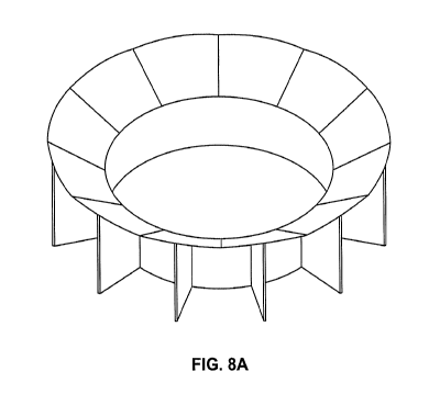
[0025] FIG. 8A gives a perspective view of the flower petal embodiment.
[0026] FIG. 8B gives a side view of the flower petal embodiment.
[0027] FIG. 8C gives a top view of the flower petal embodiment.
[0028] FIG. 8D is a sectional view along line AA in FIG. 80.
[0029] FIG. 9 is an algorithm showing how increased capture is driven in
embodiments according to teachings of the present invention.
[0030] FIG. 10 is schematic flow chart of steps according to the process
for
optimizing harvest of energy from the electromagnetic spectrum.
[0031] FIG. 11 illustrates schematically the recirculation of internal EMR
for multiple
passes through material of a cell, as demonstrated by the instant teachings.
Detailed Description
[0032] Shown herein is an electromagnetic energy capture cell that includes
a body
of material with an upper surface and a lower surface. The material may
include a glass
or other such material with a chemistry and internal shape that exhibits the
recited
properties. At least the lower surface can provide parabolic focusing as
described. The
cell preferably has an upper surface which receives electromagnetic radiation
(EMR)
into the material, the upper and lower surfaces reflect internal (EMR) back
into the
CA 02959192 2016-10-31
WO 2015/179745 PCT/US2015/032148
material, and the material substantially spans three dimensions of space
between the
upper surface and the lower surface so that the internal EMR interacts with
the material
in the three dimensions. A composition of the material e.g., in the form of
films
according to the inventive process (e.g., made via an argon purging process)
defines a
plurality of bandgaps such that wavelengths of the internal EMR outside of the
visible
spectrum excite electrons from a valance band to a conduction band. The cell
has an
internal structure or geometry with overlapping formation, i.e., a ribbon
technology or
placement energy density that generates more power than conventional PV arrays
as
shown by the data herein.
[0033] The present invention has configured an Electro-Magnetic Capture
System
which leverages the entire spectrum of such radiated energy to generate power.
[0034] The depicted electromagnetic capture system (EM-CS) covers a broader
spectrum of 200-5000EV whereas today's standard PV covers a lesser range of
800-
1100 EV. EM-CS utilizes a more dynamic Argon film as opposed to today's
standard
thin film.
[0035] EM Capturing system (EM-CS) is a new technology which captures and
converts a broad spectrum of electromagnetic radiation including forms of
ultraviolet
through and beyond infrared (C) forms of light in the realm of heat capturing.
[0036] The technologies' ability to capture a broader daily range of
electro-magnetic
radiation as such is not the same as "solar." This increased range coupled
with
increased system efficiencies delivers greater panel capacity for longer
periods of time
which results in a lower cost per Watt and greater total output.
[0037] The increased panels capacity requires significantly less surface
area
allowing panels to be installed even where space is limited and or expensive.
[0038] "Containing" or "Capturing" (used coextensively for this application)
technology generates significant cost savings over current
residential/commercial/utility
grade installations due to its smaller construction footprint and reduced
panel count
which requires significantly less real estate, installation labor, and
ancillary equipment.
[0039] EM-CS technology combined with battery storage can function as the
first
legitimate 'base load' renewable energy solution.
6
CA 02959192 2016-10-31
WO 2015/179745 PCT/US2015/032148
[0040] Appropriate for both grid-tied and off-grid system, the instant
systems provide
for de-limited usage of EM whole spectrum energy.
[0041] According to embodiments, "panels" of the instant inventions are
designed to
contain/capture and convert a larger range of Radiation of up to 2.9 kW/m3
unlike all
other panels on the market. Since, according to the present inventions, panels
use the
UV, visible and invisible light spectrums.
[0042] According to embodiments, there are disclosed multiple EM "Argon
films"
(transparent, stable, and able to absorb 200ev to 5000ev). Likewise,
proprietary glass
formulations are designed to absorb to total EM radiation spectrum (with
minimal - 6-8%
refracted light, of any type), the addition of angled silvered-apical prisms
further
increases the ability to absorb indirect EM radiation energy.
[0043] According to embodiments, double Parabolic reflecting bases directs
and
captures sunlight so the system's efficiency is maximized.
[0044] The technology allows for up to 800 percent more EM radiation,
giving more
total kW/day absorbed, depending upon Solstice and zone.
[0045] According to embodiments, the internal lining breaks up EM
radiation,
increasing absorption acting as a semi-permeable membrane allowing radiation
in but
inhibiting its exit.
[0046] The new technology increases total radiation up to 66% more than
film alone.
That is why this is an EM "system" not just another solar panel, as the prior
art
discloses.
[0047] The ability to absorb: direct, indirect, reflect, prismatic and even
diffused
energy, is likewise featured.
[0048] Internal design increases electron passage at least about 7-37
times, it is
respectfully submitted.
[0049] In contra-distinction to conventional systems where EM panels only
use part
of the EM spectrum. (Current panels use only the visible spectrum at up to 20%
of
0.6kW/m2).
[0050] The present system results from designing a system that used ALL of
the
available electro-magnetic radiation energy far exceeding the small range of
an average
7
CA 0VMM keit .10-31
WO NI 51179745 PCIIIIS211115/03214X
solar panel and even exceeding the massive available ranges of UV through IR.
This
system is designed to absorb much larger spectrums of radiation.
[0051] Existing solar panels only use 800 to 1100 wavelength, whereas the
instant
teachings use Broad Spectrum Technology which uses a much larger 200 to 5000
wavelength.
[0052] Current panels "bounce" sunlight, whereas the new EM panels
"capture" the
sun's energy, and/or "contain" much larger aliquots of the same.
[0053] The radiation rotational design increases radiation exposure up to
nearly 70%
greater than traditional models
[0054] This design uses the angle of sunlight, the rotation of the earth,
the
relationship between direct line increased time arid greater absorption to
decrease
reflected/refracted light and increase the amount of light radiation that
enters the
capture cell (Snail's Law).
[0055] In addition, the glass composition enables it to absorb indirect
light.
[0056] Additional useful background may be found in Takarnoto. 2009, Status of
multijunction solar cells and future development, CS MANTECH CONFERENCE, May
18th-21st. Tampa, FL. USA (4 pages); U.S. Pat. 8.093,492 to Hering; U.S. Pat.
6,335.480 to Bach; and U.S. Pat. 6,689.949 to Ortabasl.
[0057] The technology disclosed herein is directed toward systems and methods
for
generating energy from sources such as the sun. Embodiments of the disclosed
technology are configured so as to be able to capture a broad spectrum of
electromagnetic energy and efficiently convert that energy into electricity
for a variety of
uses. A variety of features can be included to enable efficient capture of
electromagnetic energy into increase the efficiency of the solar power
generation
system. For example, unique shapes and compositions of glass can be used to
improve
the entry arid capture of light in the system a parabolic or other like
reflecter can be
used to capture energy. such as so solar energy lrom the sun (or other source
of
electromagnetic energy) at various angles, and Multiple layers of photovoltaic
materials
at a variety of different band gaps can be combined to capture a broad
spectrum of
electromagnetic energy within and beyond the visible light spectrum.
=
CA 2959192 2017-07-04
CA 02959192 2016-10-31
WO 2015/179745 PCT/US2015/032148
[0058] An early prototype of the system includes a glass or other
transparent
enclosure, an energy conversion stack created using one or more solar
conversion
materials (i.e., photovoltaic materials) having different band gaps (bandgap
materials),
and a reflector that can be configured to redirect sunlight (or other
electromagnetic
energy from the sun) to the glass enclosure that might not otherwise impinge
on the
enclosure, so that the reflected light can be captured by the glass enclosure
and
directed toward the photovoltaic materials. These and other features and
aspects of the
disclosed technology can be utilized and combined in various combinations to
create an
efficient energy generating system. Various aspects of these features are
described in
this document by way of example. In various embodiments, the glass used to
encase
the photovoltaic materials can be formulated to increase or maximize the total
amount
of the electromagnetic radiation spectrum that reaches, and can be captured
by, the
photovoltaic materials.
[0059] The glass is tempered to improve its resistance to breakage, and is
desirable
for its broad wavelength transmission spectrum. For example, in various
embodiments,
tempered phosphate MgF and sapphire glass can be provided with a transmission
spectrum delivering approximately 80 to 90% transmission across a wavelength
of
approximately 400 to 2750 nm. In some embodiments, the glass can achieve a
high
percentage of transmission over a spectrum of approximately 200 to 5000 nm.
The
glass can be doped with a phosphorus chemical (e.g., 20% or less, although
other
doping percentages can be used) to alter the absorption of electromagnetic
energy as
well as the refractive index of the glass. The doping is done with a view to
increasing
the effective angle of acceptance of the glass such that more energy from the
sun is
accepted into the glass and less is reflected off of the surface of the glass
as compared
to non-doped glasses.
[0060] Additionally, the glass encasement is managed including
antireflective (AR)
coating on the outer surface of the glass and an oxide coating on the inner
surface of
the glass, inter alia. The antireflective coating can be added to reduce the
amount of
reflections off of the outer surface as compared to an uncoated glass. The
oxide coating
on the inner surface can be provided to perform various functions. For
example, the
oxide coating can be provided to prismatically divide the light into its
constituent spectral
9
CA 02959192 2016-10-31
WO 2015/179745 PCT/US2015/032148
components. This allows incoming light to be separated into spectral
components and
the spectral components to be directed at different directions from the inner
surface of
the glass.
[0061] The oxide coating can also act as a semi-permeable membrane,
allowing
radiation in but inhibiting its exit. This can facilitate the reuse of photons
that are not
absorbed and converted on their first pass through the materials. With the
appropriate
doping and other characteristics as described, embodiments can be implemented
that
achieve the delivery to the bandgap materials of 58.86 A of direct light
impinging on the
glass, and delivery to the bandgap materials of up to 30% of indirect light
impinging on
the glass. This can be achieved because light impinging on the glass at a
shallow angle
can be captured rather than reflected, and then can be refracted toward the
photovoltaic
bandgap materials located within the central region of the glass encasement.
[0062] According to instant teachings light impinging on the glass at a
shallow angle
can be captured rather than reflected A simple example of this is illustrated
in figure 2 in
which incoming light rays at shallow angles are accepted by and refracted
toward the
stack of photovoltaic energy conversion materials. The shape of the glass
housing is
important to increasing the efficiency of the system and the range of the
electromagnetic spectrum that can be captured by the system. The shape is not
limited
to that shown in the figures. Various shapes of glass enclosure can be used,
however,
in some embodiments, a rounded shape is used to present a more direct angle to
the
source of the electromagnetic energy (e.g., the sun, a lamp, or other energy
source)
and to facilitate refraction of the light toward the photovoltaic materials.
[0063] In one aspect, the invention provides an improved high efficiency
electromagnetic energy capturing system (EM-CS). The EM-CS includes a cell
101.
[0064] FIG. 1 shows a cell 101 of the invention. Cell 101 includes a core
member
201 and one or more end members 301.
[0065] FIGS. 2A-2C show a core member 201 of the cell 101. FIG. 2A gives a
perspective view of core member 201. FIG. 2B gives a cut-away profile view of
member
201. FIG. 2C shows a network of electrodes in core member 201. Core member 101
includes, in combination, at least a material body with an upper and lower
surface layer,
whereby the upper surface layer receives electromagnetic radiation (EMR) into
the
CA 02959192 2016-10-31
WO 2015/179745 PCT/US2015/032148
material and the upper and lower surface layers reflect internal EMR back into
the
material. The surface layer preferably includes doped glass, e.g., with MgF2
or other
suitable metal halide or such material ("proprietary glass"). The body spans
three
dimensions of space between the upper surface layers and lower surface layers
whereby the internal EMR interacts with the material in these dimensions. The
body
captures EMR traveling therein by means of the dense packed ribbon technology
defined by a plurality bandgaps whereby wavelength of the internal EMR excite
electrons from a valence band to a conduction band. The dense packed ribbon
technology includes an innermost film 205, a second film 206, a third film
207, and an
outermost film 208. In a preferred embodiment, between at least about 3 and 7
films are
included. In one embodiment each film includes one separately selected from
GaAs,
Ge, Si and GaInP2. Each film may separately include materials listed in Table
1. In
other embodiments materials such as GaS, GIP,GIA, InGa, CdTe, CIGS, CdTe/CdS,
CuInSe2, GIN, ZMT, and/or CdS, may be used. FIG. 20 illustrates electrodes in
contact
with the films of the body. An upper surface herein dubbed "proprietary glass"
of the
material body may be provided by a glass that is doped with a metal halide,
preferably
MgF2, to maximize retention of EM radiation in the cell 101. The doped upper
surface
may be outermost film 208 or is preferably a covering layer on top of the
material body.
[0066] FIG. 3 shows an end member 301 of the cell 101. End member 301
includes
hardware section 401 abutting end member 601 and supported by base section
501.
FIG. 4A gives a perspective view of the hardware section 401. FIG. 4B gives an
end
view of the hardware section 401. FIG. 40 gives a top view of the hardware
section 401.
FIG. 5A gives a perspective view of the base section 501. FIG. 5B gives an end
view of
the base section 501. FIG. 5C gives a top view of the base section 501. FIG.
6A gives a
perspective view of the end member 601. FIG. 6B gives an end view of the end
member
601. FIG. 6C gives a top view of the end member 601.
[0067] FIG. 7 shows efficiency of an EM-CS capture module such as cell 101.
A
capture module of the invention includes a capture cell with a body having a
lower
surface and a curved upper surface, both extending from a one end to the
other, where
the curved upper surface may be contoured to provide a surface approximately
normal
to the rays of the sun as the sun travels across the sky, from sunrise to
sunset.
11
CA 02959192 2016-10-31
WO 2015/179745 PCT/US2015/032148
Geometries such as this may provide up to about a 66% increase in solar
exposure
over conventional, flat or box-type solar cells. Note that because the size of
the
enclosure is very small relative to the earth, the sun does not generally
travel in a
constant arc relative to the enclosure. In some embodiments, the glass housing
can be
configured to have a smaller radius of curvature on 2 sides as compared to
across the
top of the glass housing. In other words, the housing is configured to have a
roughly
flower shaped configuration.
[0068] This can be useful to provide the capture of direct light during
times of sunrise
and sunset when energy from the sun is impinging on the glass at low angles of
inclination to the earth. In other embodiments, the glass housing is
configured in a
flower-petal like shape to present a normal surface to the sun's rays as the
sun moves
across the sky during the day.
[0069] FIGS. 8A-8D illustrate a complex shape for a "flower petal" member
for use
within a thick film/ multi film cell according to certain embodiments. FIG. 8A
gives a
perspective view of the flower petal embodiment. FIG. 8B gives a side view of
the flower
petal embodiment. FIG. 8C gives a top view of the flower petal embodiment.
FIG. 8D is
a sectional view along line AA in FIG. 80. The morphology depicted in FIG. 8A
may be
derived through the application of the algorithm illustrated by FIG. 9 to
transform vectors
of wide-spectrum incoming EM from multiple different times during a day into
orientations for thick-film like layers produced by sputtering, selenization,
annealing and
lamination. One or multiple of the petal elements may be used in combination
with each
other or with other element disclosed herein with a broad spectrum EM-CS cell.
In one
embodiment, the invention provides an EM capture cell including at least one
and
preferably at least about 3 to 7 members as shown in FIG. 8 each member
comprising a
thick film defining at least about 1 to many bandgaps by included
semiconductor
materials as listed elsewhere herein.
[0070] Complex partially spherical shapes may but need not be used, and
indeed, in
various embodiments the enclosure can be shaped to present a more direct angle
to the
sun based on the sun ' s ephemeris for a given latitude and longitude or
geographic
region of application. Daylighting models and other techniques can be used to
optimize
the shape and contour of the glass enclosure to capture a maximum amount of
energy.
12
CA 02959192 2016-10-31
WO 2015/179745 PCT/US2015/032148
[0071] FIG. 9 shows a result of combining the Lens' makers equation and
Snell's law
to show that you can refract, focus and (not reflect away) 3.5 suns of energy
into the
EM-CS, with the outer layer schematically directing the light as shown by
vectors
illustrated in the bottom panel.
[0072] FIG. 9 illustrates the use of a transformation formula to guide the
design of
surface geometries with a cell of the invention. Where (X, Y, Z) are the
coordinates of a
3D point in the world coordinate space, (u, v) are the coordinates of the
projection point
in pixels. A is called a matrix of intrinsic parameters. (cx, cy) is a
principal point (that is
usually at the image center), and fx, fy are the focal lengths expressed in
pixel-related
units. Thus, if an image from within the unit is scaled by some factor, all of
these
parameters should be scaled (multiplied/divided, respectively) by the same
factor. The
matrix of intrinsic parameters does not depend on the incoming light and, once
estimated, can be re-used (as long as the focal length is fixed). The joint
rotation-
translation matrix [NI] is called a matrix of extrinsic parameters. It is used
to describe
the motion of light source relative to cell. That is, [RN translates
coordinates of a point
(X, Y, Z) to some coordinate system, fixed with respect to the cell. Surface
of the cell
may have some distortion, mostly radial distortion and slight tangential
distortion. So,
the above model is extends as shown in FIG. 9. In FIG. 9, k 1,k 2,k 3,k 4,k
5,
k_6 are radial distortion coefficients, p_1 , p_2 are tangential distortion
coefficients.
Higher-order coefficients are not considered. In the functions shown the
coefficients are
passed or returned as (k 1, k 2, p 1, p 2[, k 3[, k 4, k 5, k 6]]) vector.
That is, if the
vector contains 4 elements, it means that k_3=0 . The distortion coefficients
do not
depend on the outside light, thus they also belong to the intrinsic cell
parameters. The
extended model shown in FIG. 9 can be used to project 3D points to the image
plane
given intrinsic and extrinsic parameters; compute extrinsic parameters given
intrinsic
parameters, a few 3D points and their projections; estimate intrinsic and
extrinsic cell
optic parameters from several views of a known calibration pattern (i.e. for
design of the
cell surface morphology); and estimate the relative position and orientation
of the thick
films and compute the rectification transformation that optimizes EM capture.
[0073] The capture cell may further comprise internal mirroring or
silvering or other
reflective coating on the bottom surface and at least a portion of the upper
surface, for
13
CA 02959192 2016-10-31
WO 2015/179745 PCT/US2015/032148
instance along the sides of the upper surface. In various example embodiments,
the
entire bottom surface may comprise a reflective coating or mirroring, as well
as
approximately two-thirds of the surface of the sides. The internal mirroring
produces a
photonic (ionic or electron) reflecting chamber, where electromagnetic
radiation entering
the capture cell reflects off the mirroring and bounces around inside the
capture cell,
creating a total internal reflection, or near total internal reflection, or a
large number of
reflections to contain photons that have entered the system. This has the
effect of
raising the likelihood that capture photons will impact the photovoltaic
material
distributed inside the capture cell.
[0074] Since mirroring in this example is confined to the bottom surface
and a
bottom portions of the side surface of the enclosure, it does not affect the
external light
penetration, diffraction, refraction or reflection; its only effect is
"capturing" of photons
once penetrated into the cell. When a photon is remains un-captured, it
ultimately
converts to heat, and heats the photovoltaic material. This increases the flow
of
electrons gathered from the photons (sometimes called the Delta-K effect by
increasing
the particle range).
[0075] The capture cell may have an optically active and non-reflective
exterior (e.g.,
using a specific formulation of soda-lime, borosilicate or phosphate glass
combination)
allowing for a high level of photon penetration while minimizing diffraction,
refraction or
reflection that may occur from the angle of penetration or/of the Earth's/Sun
solar
curvature. This design allows for the attenuation of solar radiation from
atmospheric
scattering and increases the absorption of solar radiation available at a
given location.
Current photovoltaic systems typically use thin film photovoltaic cells, which
have a very
low efficiency, utilize only a fraction of the total available photons, and
suffer from
delaminating. Various embodiments of the technology described herein utilize
thick film-
like technology for the photovoltaic materials in some embodiments, these
thick films
can be as thin as .03 nm or as thick as 5.0 microns.
[0076] Moreover, as discussed the semantics of thin or thick films are such
that
artisans understand which versions can be implemented to allow the application
of
multiple layers or multiple bandgap material in one or more passes as needed,
as
explained herein. For example, transparent Kapton/molybdenum (or other
polyimideas
14
CA 02959192 2016-10-31
WO 2015/179745 PCT/US2015/032148
needed available from DuPont, Wilmington, DE, USA such as UPILEX). A
translucent,
multi-leveled, multi-band gapped material, preferably a thick-film like-
material (or
multiple thick film band gap lattice (MTFBG) such as films 205, 206,...) may
be provided
as the photovoltaic material. In various embodiments, the material can be an
integrated
multi-junction photovoltaic cell with multiple p-n junctions made of different
semiconductor materials each having a different bandgap. In other embodiments,
the
multi-bandgap material can be made from a plurality of individual thick films,
each
having a photovoltaic material with a designated bandgap. Ideally, the stack
is made
such that each p-n junction has a different bandgap energy, and produces
current in
response to a different wavelength of the electromagnetic spectrum impinging
on the
device. This increases the conversion efficiency of the device by using more
of the
available electromagnetic spectrum.
[0077] Providing multiple materials with multiple band gaps allows the unit
to
respond to multiple different wavelengths of the spectrum. In some
embodiments, the
photovoltaic stack includes 2 to 4 layers of bandgap materials each having a
different
bandgap energy. In other embodiments, other numbers of layers of bandgap
materials
can be provided, including a single layer stack or more than 4 layers.
Marginal returns
may diminish with increasing number of layers depending on a number of factors
including, for example, the spectrum of available electromagnetic energy, the
transparency and absorption efficiency of the various materials in the stack,
the amount
of internal reflection that can be achieved to contain capture photons, and so
on. In
operation, the outer bandgap material of the photovoltaic stack captures the
photons it
can at the wavelength associated with its bandgap energy and converts those
into
electric current.
[0078] Those photons not captured by the first layer, pass through to
subsequent
layers until they are captured, absorbed, reflected off the surface of a
subsequent layer,
or pass through the stack and are reflected off of the reflective surfaces of
the glass
enclosure, A portion of the reflected photons reach the photovoltaic stack
again
providing the opportunity for these otherwise lost photons to be captured and
converted
to electric current. The multi-leveled, multi-band gapped thick film can be
bendable and
may incorporate different materials having different band gaps optimized for
different
CA 02959192 2016-10-31
WO 2015/179745 PCT/US2015/032148
wavelengths of light present in white light (including for instance
ultraviolet and infrared
light), and for different wavelengths of light that occur at different times.
For instance,
during sunrise and sunset the spectrum of light is different from that of mid-
day, so
different materials may be provided with different band gaps to capture as
much of the
energy of those different types of light as possible. In one example
embodiment the
different materials may comprise GaAs, Ge, Si and GaInP2, for instance. In
other
embodiments materials such as GaS, GIP,GIA, InGa, CdTe, GIGS, CdTe/CdS,
CuInSe2, GIN, ZMT, and/or CdS, may be used. In some embodiments, the band gaps
of the materials are selected such that there are overlapping bands to achieve
energy
conversion from the most dense regions of the spectrum. In some embodiments,
the
chemical compositions of the materials can be varied to tune the bandgaps of
the
junctions.
[0079] Table 1 illustrates another example of different materials that can
be used
along with their associated band gaps and estimated conversion efficiencies
using 2 or
more layers. Artisans understand the exemplary numbers are lowered in this
example
due to overlap.
(Zn5; ZnSe.) 3,6 eV
CGS (Cd.S; loGaAs) 2A eV 19.01%
InGaAsf) KleP; Ittleapi 1:84 eV 15:02%
CdTe (GAO L44 eV 16:06%
C-51 (404,t; 1.12 eV 18,78%
inGaAs 41-5k:it Qajnp) 0,.92 eV 9,0.5%
qpjliyhjia:Sk.Irdb} .................. . 010 eV ..
[0080] In various example embodiments two, three, four or five layers of
unique thick
films 300 may be provided that can gather photons on either side of the film,
each of
which may in certain embodiments vary from about .03 to 5.0 microns in
thickness (e.g.,
shown as films 205,206,... in FIG. 2B). The length and width of the films can
be of
suitable dimensions depending on the available dimensions and volume of the
enclosure. The length and width can also be chosen based on the manner in
which the
16
CA 02959192 2016-10-31
WO 2015/179745 PCT/US2015/032148
films are layered within the enclosure. For example, in some embodiments, the
films
can be layered in a planar or flat (or substantially flat) configuration
within the enclosure.
In other embodiments, the films can be curved or curled or wrapped, and
layered within
the enclosure in a coaxial or substantially coaxial fashion. For example,
flexible layers
can be used with sufficient resilience such that when inserted into the
enclosure they
conform to the inner contour of the enclosure. Accordingly, the films can be
configured
to take the shape of the enclosure. Where design issues have traditionally
been seen to
limit the width of the film, ribbon-like lengths of film can be wound (e.g. in
a helical
fashion) within one another inside the enclosure. The multiple-layer
translucent
photovoltaic stack may be electrically connected with a positive charge for
ionic
collection. The multiple-layer translucent photovoltaic stack may be at least
partially
surrounded by internal mirroring, as described above with respect to FIGS. 1,
2 and 3.
This unique film technology allows bidirectional photovoltaic pathway (i.e.,
energy
conversion from the top down and from the bottom up).
[0081] As noted above, in various embodiments the multiple layers of
bandgap
materials can be fabricated whether as an integrated device or as individual
sheets,
using thick film technology. In examples, polyamides, a thick film substrate
such as
Mylar, KAPTON, or any other polyimide film (available from DuPont, Wilmington,
DE,
USA), or other film can be used as a substrate, such materials are available
in varying
degrees of transparency. The substrate sheet can be run through a deposition
device
(e.g. using chemical vapor deposition or CVD) or other like device in which
the layers of
the device are deposited onto the substrate. In addition to chemical vapor
deposition,
other techniques such as, for example, Extrusion Positive Printing, VPD,
Sputtering,
and the like can be used to lay down the various layers.
[0082] For example, in such a process the electrode layers and
semiconductor
layers can be deposited onto the substrate to produce the thick film
photovoltaic
material. The fabrication device can be maintained with a positive pressure
using an
inert gas such as, for example, argon, to keep the chamber relatively free or
completely
free of oxygen. This can avoid the detrimental effects of oxidation on the
materials.
Where bandgap materials are fabricated on individual sheets, a single junction
device
can be fabricated on a given substrate.
17
CA 02959192 2016-10-31
WO 2015/179745 PCT/US2015/032148
[0083] On the other hand, wherein hetero junction device is desired,
multiple
bandgap materials can be deposited onto a single substrate. Where desired,
indium tin
oxide, graphing, or other like materials can be used to create transparent
electrodes.
The various aspects of the disclosed technology may be used individually or in
various
combinations, including in complete energy conversion systems comprising: a
capture
cell (in which photons may be more completely retained giving rise to a
greater degree
of energy absorption and conversion); a multi-layered photovoltaic system, a
unique
thick-film processing technology; the utilization of multigap material for
greater access to
the light spectrum (hence greater exposure and greater absorption of photons);
and with
a multi-dimensional core for use with nanotechnology is being (dots, lattice)
GPS and
various sensor, storage usages and ozone creation. In addition, the ability to
capture
indirect lighting from the angle and type of glass formulations increases the
total overall
energy wattage of the system. The use of capture cells with multiple levels of
collecting
film 300 may incorporate all of the above technologies to create a multi-
layered, multi-
band gap, bidirectional photovoltaic film core. The capture cell can work with
the thick
film by increasing the amount of light exposure that can provide photonic
absorption,
and by increasing the number of photon passes through the band gap material.
[0084] The thick film avoids problems in thin film technology; it is more
stable and
still allows for transparency for photons to pass through multiple absorption
layers with
multiple band gap materials. The present photovoltaic system can be used to
generate
a flow of electrons (an electric current) where there is sunlight or another
source of
electromagnetic radiation or waves. The present photovoltaic system can be
used on or
in homes, commercial buildings, industrial applications, automobiles, or any
other form
of transportation. The system can be portable, as it is highly efficient and
can be used
anywhere that energy is needed. The band gap of a material is the energy
required to
excite an atom of that material sufficiently to move one of its electrons from
a lower
energy state, or band, to a higher energy state, or band.
[0085] Only photons with energy levels greater than that of the band gap
can excite
electrons to move from the valence band to the conduction band, where they can
flow
and create electricity. For materials with lower band gaps, a greater range of
light
frequencies will have sufficiently high energies to excite electrons in those
materials to
18
CA 02959192 2016-10-31
WO 2015/179745 PCT/US2015/032148
move from the valence band to the conduction band (this helps determine
Valence band
material). Moreover, there are various "tunable" materials, such as InGap or
CIGS.
Therefore, the smaller the band gap of a material, the more easily light
striking that
material may be converted to electricity. But when the band gap is too small,
the
negatively-charged electrons in the conduction band recombine too easily with
the
positively-charged atoms they left behind (i.e., "holes"), such that
maintaining a flow of
electrons (i.e., an electrical current) becomes difficult.
[0086] Because different frequencies of light carry different levels of
energy,
materials with different band gaps may be provided to capture the different
frequencies
of light within a spectrum to optimize the total amount of energy obtainable
from the
spectrum. Band gaps are selected that are not only efficient at a certain
wavelength, but
also that gather the most total electrons, keeping in mind that higher
frequency light
carries more energy. Some examples of band gaps are: Silicon's band gap is
1.11-1.12
eV; Selenium's is 1.5-1.6 eV; GaAs Gallium/Arsenic's is 1.3-1.4 eV; CuO
cupric/Oxide '
s is 2.0 eV; GaTe is 1.4 eV; AlAs Aluminum/Arsenic 's is 2.3 eV. Light also
has specific
unique wavelengths.
[0087] For example, Red is 622-780 nm; Orange is 622-597 nm; Infrared A is
700-
1400 nm; Infrared B is 1400-3000 nm; and Infrared C is 3000-10000 nm.
Accordingly,
Silicon could theoretically convert 100% of the photons having a wavelength
equivalent
to its 1.11-1.12 eV band gap, while also converting a lower percentage of
photons
having a shorter wavelength and higher energy. However, photons of light
having a
wavelength over 1.12 eV will not generate any electricity in Silicon, because
these
longer wavelength photons have less than the minimum level of energy needed to
overcome Silicon 's 1.11-1.12 eV band gap.
[0088] In practice, conventional solar cells using Silicon have had actual
conversion
efficiencies ranging from about 12% to 14%. That is, only about 12% to about
14% of
the energy in the photons hitting conventional Silicon solar cells is
converted to
electricity (the same range as Hoffman produced in 1960 or 54 years ago). The
use of
tunable PV material, i.e., InGS(N)(P), GIGS, GaAs, AlGeN, changes this. By
pushing
the formula higher in the Se one can manipulate both the band gap and adjust
for the
"holes." Hence, if using Si provides a range of at least about 1,112 -800 ev
(with the
19
CA 02959192 2016-10-31
WO 2015/179745 PCT/US2015/032148
latter giving way to more holes) then one can tune the other separate layers
to cover
850-600 and 650-315, thus, covering the highest gradient of energy (from IRc-
UVb).
[0089] True efficiency considers the range of energy covered; efficiency of
said
range converted; and duration of energy focused. What plays into this is angle
internal
mirroring (capturing) reduced reflection/refraction. Prototypes were tested
using
combinations of Indium, Gallium and nitrogen (Inl-xGaxN), which together
convert
virtually the entire spectrum of sunlight, including ultraviolet, infrared and
some limited
portion of the x-ray spectrum. These materials were doped with Cadmium
telluride
(CdTe) and Copper Indium gallium selenide (COS), CdTe/CdS, CuInSe2 (copper
indium selenide- CIS), Gallium Indium Nitride (GIN); Zinc Manganese Telluride
(ZMT);
Cadmium sulfide (CdS).
[0090] FIG. 10 diagrams methods of the invention. The flow chart of steps
shows a
process for optimizing harvest of energy from the electromagnetic spectrum.
[0091] FIG. 11 illustrates the recirculation of internal EMR for multiple
passes
through material of a cell, likewise photons sourced from direct, indirect,
reflected,
prismatic and diffused energy are housed and energy derived from same,
according to
the instant EM-CS.
[0092] Furthermore, the described features, structures, or characteristics
of the
invention may be combined in any suitable manner in one or more embodiments.
In the
following description, numerous specific details are provided to provide a
thorough
understanding of embodiments of the invention. One skilled in the relevant art
will
recognize, however, that the invention may be practiced without one or more of
the
specific details, or with other methods, components, materials, and so forth.
In other
instances, well-known structures, materials, or operations are not shown or
described in
detail to avoid obscuring aspects of the invention.
[0093] Any schematics and/or flow chart diagrams along with verbal
descriptions of
steps, included herein are generally set forth as either linguistic or
pictorial logical flow
chart diagrams. As such, the depicted order and labeled steps are indicative
of one
embodiment of the presented method. Other steps and methods may be conceived
that
are equivalent in function, logic, or effect to one or more steps, or portions
thereof, of
the illustrated systems, processes or methods.
4:A Gr1,5919? 203,-111-31
WO 200/179745 1711S2015/032148
[0094] Additionally, any format and/or symbols employed are provided to
explain the
logical steps at associated systems, processes and methods and are understood
not to
limit the scope 01 the method. Although various arrow types and line types may
be
employed in the flow chart diagrams. they are understood not to limit the
scope of the
corresponding method. Indeed, some arrows or other connectors may be used to
indicate only the logical flow of the method. For instance, an arrow may
indicate a =
waiting or monitoring period of unspecified duration between enumerated steps
of the
depicted method. Additionally, the order in which a step is suggested does not
indicate
that it needs to be performed prior to or after another step unless expressly
set forth.
[0095] =
[0096] Legacy or historical attempts to address these issues also have some
value,
in defining the state of the art, and paucity of improved applications to
overcome the
science.
[0097] While methods, devices, compositions, and the like, have been described
in
terms of what are presently considered to be the most practical and preferred
implementations, it is to be understood that the disclosure need not be
limited to the
disclosed implementations. It is intended to cover various modifications and
similar
arrangements included within the spirit and scope of the claims, the scope of
which
should be accorded the broadest interpretation so as to encempass all such
modifications and similar structures. The present disclosure includes any and
all
implementations of the following claims. It is understood that the term,
present
disclosure, in the context ol a description of a component. characteristic, or
step, of one
particular embodiment of the disclosure, does not imply or mean that all
embodiments
of the disclosure comprise that particular component, characteristic, or step.
[0098] It should also be understood that a variety of changes may be made
without
departing from the essence of the disclosure. Such changes are also implicitly
included
21
CA 2959192 2017-07-04
U:',5VIIN. IU. %I
WO 2015/179745 INS2015/113214X
in the description. They still fall within the scope of this disclosure. It
should be
understood that this disclosure, isintended to yield a patent covering
numerous aspects
of the disclosure both independently and as an overall system and in both
method and
apparatus modes.
[0099] Further, each of the various elements of the disclosure and claims
may also
be achieved in a variety of manners. I his disclosure should be understood to
encompass each such variation, be it a variation of an implementation of any
apparatus
implementation, a rnethoo or process implementation, or even merely a
variation of any
element of these.
[0100] Particularly, it should be understood that as the disclosure relates
to elements
of the disclosure, the words for each element may be expressed by equivalent
apparatus terms or method terms -- even if only the function or result is the
same.
[0101] Such equivalent, broader, or even more generic terms should be
considered
to be encompassed in the description of each element or action. Such terms can
be
substituted where desired to make explicit the implicitly broad coverage to
which this
disclosure is entitled.
[0102] It should be understood that all actions may be expressed as a means
for
taking that action or as an element which causes that action.
[0103] Similarly, each physical element disclosed should be understood to
encompass a disclosure of the action which that physical element facilitates.
[0104)
[0105J To the extent that insubstantial substitutes are made. to the extent
that the
applicant did not in fact draft any claim so as to literally encompass any
particular
implementation. and to the extent otherwise applicable, the applicant should
not be
understood to have in any way intended to or actually relinquished such
coverage as
the applicant simply may not have been able to anticipate all eventualities:
one skilled in
= the art, should not be reasonably expected to have drafted a claim that
would have
literally encompassed such alternative implementations.
[0106] Further, the use of the transitional phrase "comprising" is used to
maintain the
"open-end" claims herein, according to traditional claim interpretation. Thus.
unless the
22
=
CA 2959192 2017-07-04
CA 02959192 2016-10-31
WO 2015/179745 PCT/US2015/032148
context requires otherwise, it should be understood that the term "comprise"
or
variations such as "comprises" or "comprising", are intended to imply the
inclusion of a
stated element or step or group of elements or steps but not the exclusion of
any other
element or step or group of elements or steps. Such terms should be
interpreted in their
most expansive forms so as to afford the applicant the broadest coverage
legally
permissible.
23