Note: Descriptions are shown in the official language in which they were submitted.
DESCRIPTION
TITLE OF INVENTION
Converter and Power Conversion Device Manufactured using the Same
TECHNICAL FIELD
The present invention relates to a converter and a power conversion device
manufactured using the converter, and particularly to a converter configured
to convert
an alternating-current (AC) voltage into first to third direct-current (DC)
voltages, and a
power conversion device manufactured using the converter.
BACKGROUND ART
Japanese Patent Laying-Open No. 2011-78296 (PTD 1) discloses a converter
including four transistors and four diodes, and configured to convert an AC
voltage into
a high voltage, a low voltage and an intermediate voltage. According to this
converter,
among four diodes, each of two diodes performing a reverse recovery operation
is
formed of a wide band gap semiconductor, thereby reducing recovery loss. Also,
each
of two diodes not performing a reverse recovery operation is formed of a
semiconductor other than such a wide band gap semiconductor, thereby reducing
cost.
CITATION LIST
PATENT DOCUMENT
PTD 1: Japanese Patent Laying-Open No. 2011-78296
SUMMARY OF INVENTION
In the conventional converter, however, four transistors have been formed of
the
same type of semiconductor, still leading to higher loss and higher cost
Therefore, a main object of the present invention is to provide a converter
with
reduced loss and cost, and a power conversion device manufactured using the
converter.
A converter according to the present invention is configured to convert an AC
voltage applied to an input terminal into a first DC voltage, a second DC
voltage and a
- 1 -
CA 2959475 2018-03-26
third DC voltage, and output the first DC voltage, the second DC voltage and
the third
DC voltage through a first output terminal, a second output terminal and a
third output
terminal, respectively. The converter includes: a first transistor having a
first
electrode and a second electrode that are connected to the first output
terminal and the
input terminal, respectively; a second transistor having a first electrode and
a second
electrode that are connected to the input terminal and the second output
terminal,
respectively; a first diode and a second diode connected in anti-parallel to
the first
transistor and the second transistor, respectively; and a first bidirectional
switch
connected between the input terminal and the third output terminal. The first
DC
voltage is higher than the second DC voltage, and the third DC voltage is an
intermediate voltage between the first DC voltage and the second DC voltage.
The
first bidirectional switch includes a third transistor, a fourth transistor, a
third diode,
and a fourth diode. Each of the first diode, the second diode, the third
transistor, and
the fourth transistor is formed of a wide band gap semiconductor. Each of the
third
diode, the fourth diode, the first transistor, and the second transistor is
formed of a
semiconductor other than the wide band gap semiconductor. Each of the first
diode and the
second diode being greater in rated current than each of the third diode, the
fourth diode,
the first transistor the second transistor, the third transistor, and the
fourth transistor.
According to another aspect of the present invention, there is provided a
power
conversion device comprising:
the converter as described herein; and
an inverter configured to
convert the first DC voltage, the second DC voltage and the third DC
voltage applied to the first output terminal, the second output terminal and
the
third output terminal, respectively, into a three-level AC voltage, and
output the three-level AC voltage through a fourth output terminal,
the inverter including
a fifth transistor having a first electrode and a second electrode that are
connected to the first output terminal and the fourth output terminal,
respectively,
- 2 -
CA 2959475 2018-03-26
a sixth transistor having a first electrode and a second electrode that are
connected to the fourth output terminal and the second output terminal,
respectively,
a fifth diode and a sixth diode that are connected in anti-parallel to the
fifth transistor and the sixth transistor, respectively, and
a second bidirectional switch connected between the third output terminal
and the fourth output terminal,
the second bidirectional switch including a seventh transistor, an eighth
transistor,
a seventh diode, and an eighth diode,
each of the fifth transistor, the sixth transistor, the seventh diode, and the
eighth
diode being formed of a wide band gap semiconductor, and
each of the seventh transistor, the eighth transistor, the fifth transistor,
the fifth
diode, and the sixth diode being formed of a semiconductor other than the wide
band gap
semiconductor.
In the converter according to the present invention, the first and second
diodes
performing a reverse recovery operation, and the third and fourth transistors
switching
a current each are formed of a wide band gap semiconductor, so that the
switching loss
and the recovery loss may be reduced. Also, the third and fourth diodes not
performing a reverse recovery operation, and the first and second transistors
not
switching a current each are formed of a semiconductor other than a wide band
gap
semiconductor, so that the cost may be reduced.
BRIEF DESCRIPTION OF DRAWINGS
Fig. 1 is a circuit block diagram showing the configuration of a converter
according to the first embodiment of the present invention.
Fig. 2 is a time chart showing waveforms of four PWM signals that control four
transistors, respectively, shown in Fig. I.
- 2a -
CA 2959475 2018-03-26
CA 02959475 2017-02-27
Fig. 3 is a circuit diagram for illustrating a current flowing through a
converter
shown in Fig. 1.
Fig. 4 is a time chart showing the current flowing through the converter shown
in Fig. 1.
Fig. 5 is a time chart for illustrating switching loss in each of two types of
transistors shown in Fig. 1.
Fig. 6 is a block diagram showing the configuration of a semiconductor module
included in the converter shown in Fig. 1.
Fig. 7 is a circuit block diagram showing the configuration of an
uninterruptible
power supply device including the converter shown in Fig. I.
Fig. 8 is a circuit block diagram showing a modification of the first
embodiment.
Fig. 9 is a circuit block diagram showing another modification of the first
embodiment.
Fig. 10 is a circuit block diagram showing still another modification of the
first
embodiment.
Fig. 11 is a circuit block diagram showing the configuration of a converter
according to the second embodiment of the present invention.
Fig. 12 is a circuit block diagram showing the configuration of a converter
according to the third embodiment of the present invention.
Fig. 13 is a circuit block diagram showing the configuration of an inverter
included in an uninterruptible power supply device according to the fourth
embodiment
of the present invention.
Fig. 14 is a time chart showing waveforms of four PWM signals controlling
four transistors, respectively, shown in Fig. 13.
Fig. 15 is a circuit diagram for illustrating a current flowing through the
inverter
shown in Fig. 13.
Fig. 16 is a time chart showing the current flowing through the inverter shown
in Fig. 13.
Fig. 17 is a block diagram showing the configuration of a semiconductor
- 3 -
CA 02959475 2017-02-27
module included in the inverter shown in Fig. 13.
Fig. 18 is a circuit block diagram showing a modification of the fourth
embodiment.
Fig. 19 is a circuit block diagram showing another modification of the fourth
embodiment.
Fig. 20 is a circuit block diagram showing still another modification of the
fourth embodiment.
Fig. 21 is a circuit block diagram showing the configuration of an inverter
according to the fifth embodiment of the present invention.
Fig. 22 is a circuit block diagram showing the configuration of an inverter
according to the sixth embodiment of the present invention.
DESCRIPTION OF EMBODIMENTS
[First Embodiment]
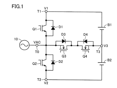
Fig. 1 is a circuit block diagram showing the configuration of a converter
according to the first embodiment of the present invention. In Fig. 1, this
converter
includes an input terminal TO, output terminals TI to 13, transistors Q1 to
Q4, and
diodes D1 to D4.
Input terminal TO receives an AC voltage VAC of a commercial frequency, for
example, from a commercial AC power supply 10. A battery B1 has a positive
electrode and a negative electrode that are connected to output terminals Ti
and T3,
respectively. A battery B2 has a positive electrode and a negative electrode
that are
connected to output terminals 13 and 12, respectively. Each of batteries B1
and B2
stores DC power. Batteries B1 and B2 are charged with the same DC voltage.
Voltages on output terminals Ti, 12 and T3 are defined as DC voltages V1, V2,
and
V3, respectively, which leads to conditions of V1 > V3 > V2 and V3 =
(V1+V2)/2.
This converter serves to convert AC voltage VAC, which has been applied to
input
terminal TO, into DC voltages Vito V3, and outputs the converted DC voltages
VI to
V3 through output terminals T1 to 13. In addition, when output terminal T3 is
grounded, DC voltages V1, V2 and V3 are to be set at a positive voltage, a
negative
- 4 -
CA 02959475 2017-02-27
voltage and OV, respectively.
Each of transistors Q1 and Q2 is an insulated gate bipolor transistor (IGBT)
formed using Si (silicon) that is a semiconductor other than a wide band gap
semiconductor. The rated current in each of transistors Ql and Q2 is 300A, for
example.
Each of transistors Q3 and Q4 is an N-channel MOS transistor formed using
SiC (silicon carbide) that is a wide band gap semiconductor. The rated current
in each
of transistors Q3 and Q4 is 500A, for example.
Each of diodes Dl and D2 is a Schottky barrier diode formed using SiC (silicon
carbide) that is a wide band gap semiconductor. The rated current in each of
diodes
D1 and D2 is, for example, 600A that is greater than the rated current in each
of
transistors Q1 to Q4 and diodes D3 and D4.
Each of diodes D3 and D4 is formed using Si (silicon) that is a semiconductor
other than a wide band gap semiconductor. The rated current in each of diodes
D3
and D4 is 450A, for example.
In this way, transistors Q1 and Q2 are different in specification from
transistors
Q3 and Q4, and diodes Dl and D2 are different in specification from diodes D3
and D4,
the reason for which will be described later.
Transistor Q1 has: a collector (the first electrode) connected to output
terminal
Ti (the first output terminal); and an emitter (the second electrode)
connected to input
terminal TO. Diode DI has: an anode connected to input terminal TO; and a
cathode
connected to output terminal Ti. In other words, diode D1 is connected in anti-
parallel to transistor Ql.
Transistor Q2 has: a collector (the first electrode) connected to input
terminal
TO; and an emitter (the second electrode) connected to output terminal T2 (the
second
output terminal). Diode D2 has: an anode connected to output terminal T2; and
a
cathode connected to input terminal TO. In other words, diode D2 is connected
in
anti-parallel to transistor Q2.
Transistors Q3 and Q4 have: drains (the second electrodes) that are connected
- 5 -
CA 02959475 2017-02-27
to each other; and sources (the first electrodes) that are connected to input
terminal TO
and output terminal 13 (the third output terminal), respectively. Diodes D3
and D4
have: cathodes that are connected to drains of transistors Q3 and Q4,
respectively; and
anodes that are connected to input terminal TO and output terminal T3,
respectively.
In other words, diodes D3 and D4 are connected in anti-parallel to transistors
Q3 and
Q4, respectively. Transistors Q3, Q4 and diodes D3, D4 form the first
bidirectional
switch.
Then, the operation of this converter will be hereinafter described.
Transistors
Q1 to Q4 have gates to which PWM signals 4)1 to 4)4, respectively, are
supplied. Figs.
2(a) to 2(e) each show a method of generating PWM signals 4)1 to o4, and
waveforms.
Specifically, Fig. 2(a) shows waveforms of a sinusoidal wave command value
signal
CM, a positive-side triangular wave carrier signal CAI and a negative-side
triangular
wave carrier signal CA2. Figs. 2(b), 2(c), 2(d), and 2(e) show the waveforms
of
PWM signals 4)1, 4)3, 4)4, and 4)2, respectively.
In Figs. 2(a) to 2(e), the frequency of sinusoidal wave command value signal
CM is a commercial frequency, for example. The phase of sinusoidal wave
command
value signal CM is the same as the phase of AC voltage VAC of the commercial
frequency, for example. Carrier signals CAI and CA2 show the same cycle and
the
same phase. The cycles of carrier signals CA1 and CA2 are sufficiently smaller
than
, 20 the cycle of sinusoidal wave command value signal CM.
The high-low levels of sinusoidal wave command value signal CM and
positive-side triangular wave carrier signal CAI are compared with each other.
When
the level of sinusoidal wave command value signal CM is higher than the level
of
positive-side triangular wave carrier signal CA!, PWM signals 4)1 and 4)4 are
set at an
"H" level and an "L" level, respectively. When the level of sinusoidal wave
command
value signal CM is lower than the level of positive-side triangular wave
carrier signal
CA1, PWM signals 4)1 and 4)4 are set at an "L" level and an "H" level,
respectively.
Accordingly, in a time period during which the level of sinusoidal wave
command value signal CM is positive, PWM signals 4)1 and o4 are alternately
set at an
- 6 -
CA 02959475 2017-02-27
"H" level in synchronization with carrier signal CA I, and thus, transistors
Q1 and Q4
are alternately turned on. Furthermore, in a time period during which the
level of
sinusoidal wave command value signal CM is negative, PWM signals (1)1 and 4)4
are
fixed at an "L" level and an "H" level, respectively, and thus, transistor Q1
is fixed in
the OFF state while transistor Q4 is fixed in the ON state.
The high-low levels of sinusoidal wave command value signal CM and
negative-side triangular wave carrier signal CA2 are compared with each other.
When
the level of sinusoidal wave command value signal CM is higher than the level
of
positive-side triangular wave carrier signal CA2, PWM signals (1)2 and 4)3 are
set at an
"L" level and an "H" level, respectively. When the level of sinusoidal wave
command
value signal CM is lower than the level of positive-side triangular wave
carrier signal
CA2, PWM signals 4)2 and 4)3 are set at an "H" level and an "L" level,
respectively.
Therefore, in a time period during which the level of sinusoidal wave command
value signal CM is positive, PWM signals 4)2 and 0 are fixed at an "L'' level
and an
"H" level, respectively, and thus, transistor Q2 is fixed in the OFF state
while transistor
Q3 is fixed in the ON state. Furthermore, in a time period during which the
level of
sinusoidal wave command value signal CM is negative, PWM signals 4)2 and 4)3
are
alternately set at an "H" level in synchronization with carrier signal CA2,
and thus,
transistors Q2 and Q3 are alternately turned on.
The ratio between the time in which the PWM signal is set at an "H" level
within one cycle and the time of one cycle of the PWM signal is referred to as
a duty
ratio. In a time period during which the level of sinusoidal wave command
value
signal CM is positive, the duty ratio of PWM signal 4)1 is maximized in the
vicinity of a
positive peak (90 degrees) of sinusoidal wave command value signal CM. Also,
the
duty ratio of PWM signal (1)1 decreases with increasing distance from the
peak, and
reaches 0 in the vicinity of 0 degree and 180 degrees. The duty ratio of PWM
signal
411 is fixed at 0 in a time period during which sinusoidal wave command value
signal
CM is negative. PWM signal o4 is a complementary signal of PWM signal 0 .
- 7 -
CA 02959475 2017-02-27
The duty ratio of PWM signal 4)2 is fixed at 0 in a time period during which
the
level of sinusoidal wave command value signal CM is positive. The duty ratio
of
PWM signal 4)2 is maximized in the vicinity of a negative peak (270 degrees)
of
sinusoidal wave command value signal CM. Also, the duty ratio of PWM signal
4)2
decreases with increasing distance from the peak, and reaches 0 in the
vicinity of 180
degrees and 360 degrees. PWM signal 43 is a complementary signal of PWM signal
412.
Then, the current flowing through each of transistors QI to Q4 and diodes D1
to
D4 during the operation of the converter will be hereinafter described. As
shown in
Fig. 3, the current flowing from output terminal Ti into input terminal TO is
defined as
11; the current flowing from input terminal TO into output terminal T2 is
defined as 12;
the current flowing from output terminal T3 into input terminal TO is defined
as 13; and
the current flowing from input terminal TO into output terminal 13 is defined
as 14.
Figs. 4(a) to 4(i) are time charts each showing the operation of the
converter.
Specifically, Fig. 4(a) shows waveforms of sinusoidal wave command value
signal CM,
positive-side triangular wave carrier signal CA1 and negative-side triangular
wave
carrier signal CA2. Figs. 4(b), 4(d), 4(0, and 4(h) show waveforms of PWM
signals
4)1, 43, (1)4, and 4)2, respectively, and Figs. 4(c), 4(e), 4(g), and 4(i)
show waveforms of
currents Ii, 13, 14, and 12, respectively. Among currents II to 14, a positive
current
= shows the current flowing through transistor Q while a negative current
shows the
current flowing through diode D. The figures also show the case where the
power
factor is 1.0, in which the phase of sinusoidal wave command value signal CM
matches
with the phase of AC voltage VAC.
In Figs. 4(a) to 4(i), in a time period during which the level of sinusoidal
wave
command value signal CM is positive, PWM signals 43 and 4)2 are fixed at an
"H"
level and an "L" level, respectively, and PWM signals 4)1 and 4)4 are
alternately set at
an "H" level. Accordingly, transistors Q3 and Q2 are fixed in an ON state and
an OFF
state, respectively, and transistors QI and Q4 are alternately turned on.
Thus, a
current flows from input terminal TO alternately into output terminals Ti and
T3.
-8-
CA 02959475 2017-02-27
During this time period, when transistor Q4 is turned off, current II of the
level
corresponding to the level of AC voltage VAC flows from input terminal TO
through
diode D1 into output terminal Ti; and when transistor Q4 is turned on, current
14 of the
level complementing current Il flows on a passage extending from input
terminal TO
through transistors Q3 and Q4 to output terminal T3.
Since transistor Q2 is fixed in the OFF state, a current does not flow through
transistor Q2, so that switching loss does not occur in transistor Q2.
Although
transistor Q1 is turned on/off, a current flows through diode Dl and a current
does not
flow through transistor Q1, so that switching loss does not occur in
transistor Ql.
Since transistor Q3 is fixed in the ON state, a current flows through
transistor Q3, but
switching loss does not occur in transistor Q3. Accordingly, during this time
period,
among diodes DI to D4 and transistors Q1 to Q4, the current flowing through
diode DI
shows the largest effective value while the greatest switching loss occurs in
transistor
Q4.
Each time transistor Q4 is changed from the OFF state to the ON state, a
reverse
bias voltage is applied to diode D1, and this diode DI performs a reverse
recovery
operation. No current flows through diodes D2 and D4 during this time period.
In a time period during which the level of sinusoidal wave command value
signal CM is negative, PWM signals 04 and 01 are fixed at an "H" level and an
level, respectively, and PWM signals 02 and 1113 are alternately set at an "H"
level.
Accordingly, transistors Q4 and Q I are fixed in the ON state and the OFF
state,
respectively, and transistors Q2 and Q3 are alternately turned on, and thus, a
current
flows alternately from output terminals T2 and T3 into input terminal TO.
During this time period, when transistor Q3 is turned off, current 12 of the
level
corresponding to the level of AC voltage VAC flows from output terminal T2
through
diode D2 into input terminal TO; and when transistor Q3 is turned on, current
13 of the
level complementing current 12 flows through a passage extending from output
terminal T3 via transistors Q4 and Q3 to output terminal TO.
Since transistor Q1 is fixed in the OFF state, a current does not flow through
- 9 -
CA 02959475 2017-02-27
transistor Ql, and thus, switching loss does not occur in transistor Ql.
Although
transistor Q2 is turned on/off, a current flows through diode D2 while a
current does
not flow through transistor Q2, with the result that switching loss does not
occur in
transistor Q2. Since transistor Q4 is fixed in the ON state, a current flows
through
transistor Q4, but switching loss does not occur in transistor Q4.
Accordingly, during
this time period, among diodes DI to D4 and transistors Ql to Q4, the current
flowing
through diode D2 shows the largest effective value, and the greatest switching
loss
occurs in transistor Q3.
Furthermore, each time transistor Q3 is changed from the OFF state to the ON
state, a reverse bias voltage is applied to diode D2, and this diode D2
performs a
reverse recovery operation. Also, no current flows through other diodes D1 and
D3
during this time period.
In summary, a large current flows through diodes D1 and D2, and these diodes
D1 and D2 each perform a reverse recovery operation. A current flowing through
diodes D3 and D4 is smaller than the current flowing through diodes D1 and D2,
and
thus, these diodes D3 and D4 each do not perform a reverse recovery operation.
No
current flows through transistors Q1 and Q2, so that switching loss does not
occur in
transistors Q1 and Q2. A current flows through transistors Q3 and Q4, so that
switching loss occurs in transistors Q3 and Q4.
Thus, as described above, as transistors Q3 and Q4, an N-channel MOS
transistor is employed that is formed of SiC as a wide band gap semiconductor
and that
has a rated current of a large value (for example, 500A), thereby reducing
switching
loss. Furthermore, as transistors Q1 and Q2, an IGBT is employed that is
formed of
Si as a semiconductor other than a wide band gap semiconductor and that has a
rated
current of a small value (for example, 300A), thereby reducing cost.
As diodes D1 and D2, a Schottky barrier diode is employed that is formed of
SiC as a wide band gap semiconductor and that has a rated current of a large
value (for
example, 600A), thereby reducing recovery loss during the reverse recovery
operation.
As diodes D3 and D4, a diode is employed that is formed of Si as a
semiconductor
- 10 -
CA 02959475 2017-02-27
other than a wide band gap semiconductor and that has a rated current of a
small value
(for example, 450A), thereby reduction cost.
Fig. 5(a) is a time chart showing the switching operation of an N-channel MOS
transistor formed using Si (which will be referred to as a Si transistor).
Fig. 5(b) is a
time chart showing the switching operation of an N-channel MOS transistor
formed
using SiC (which will be referred to as a SiC transistor).
In Figs. 5(a) and 5(b), in the initial state, a gate signal (not shown) is set
at an
"H" level to turn on the transistor, to cause a fixed current Ito flow through
the
transistor, in which case a drain-source voltage Vds is set at OV. When the
gate signal
is lowered from an "H" level to an "L" level at a certain time to turn off the
transistor,
current I decreases and voltage Vds increases.
As apparent from Figs. 5(a) and 5(b), a time period Ta in the Si transistor
from
when current I starts to fall until when current I reaches OA is longer than a
time period
Tb in the SiC transistor from when current I starts to fall until when current
I reaches
OA. In the Si transistor, current I decreases quickly until this current I
reaches a
certain value. From this certain value, however, it takes long for current Ito
reach OA.
The current flowing in a time period during which this current reaches OA from
such a
certain value is referred to as a tail current.
On the other hand, in the SiC transistor, current I decreases immediately and
some overshoot occurs. The switching loss in the transistor is represented by
a
product of current I and voltage Vds, which corresponds to an area of the
diagonally
shaded region in the figure. Accordingly, the switching loss in the SiC
transistor is
smaller than the switching loss in the Si transistor.
Fig. 6 is a diagram showing the external appearance of the converter shown in
Fig. I. In Fig. 6, the converter includes one semiconductor module Ml.
Semiconductor module Ml is provided on its inside with transistors Q1 to Q4
and
diodes D1 to D4. Semiconductor module MI is provided on its outside with an
input
terminal TO and output terminals T1 to 13. Furthermore, semiconductor module
Ml
is provided on its outside with four signal terminals used for supplying PWM
signals
- 11 -
CA 02959475 2017-02-27
(1)1 to (1)21 to the gates of transistors QI to Q4, respectively, but these
four signal
terminals are not shown for simplification of illustration of the figure.
Fig. 7 is a circuit block diagram showing the configuration of an
uninterruptible
power supply device including the converter shown in Fig. 1. In Fig. 7, the
uninterruptible power supply device includes an input filter 1, a converter 2,
a DC
positive bus LI, a DC negative bus L2, a DC neutral point bus L3, capacitors
Cl, C2,
an inverter 3, an output filter 4, and a controller 5.
Input filter 1 serves as a low pass filter to allow the AC power of a
commercial
frequency from commercial AC power supply 10 to flow into input terminal TO of
converter 2, and to prevent the signal of a carrier frequency generated in
converter 2
from passing through to commercial AC power supply 10.
DC positive bus LI, DC negative bus L2 and DC neutral point bus L3 have: one
ends connected to output terminals Ti, T2 and T3, respectively, of converter
2; and the
other ends connected to three input terminals, respectively, of inverter 3.
Capacitor
Cl is connected between buses LI and L3 while capacitor C2 is connected
between
buses L3 and L2. Buses Li and L3 are connected to the positive electrode and
the
negative electrode, respectively, of battery B1 while buses L3 and L2 are
connected to
the positive electrode and the negative electrode, respectively, of battery
B2.
As shown in Fig. 1, converter 2 includes an input terminal TO, output
terminals
TI to T3, transistors Q1 to Q4, and diodes DI to D4, and is controlled by PWM
signals
4)1 to 44 from controller 5.
In the normal situation in which AC power is normally supplied from
commercial AC power supply 10, converter 2 converts the AC power supplied from
commercial AC power supply 10 through input filter 1 into DC power, and
supplies the
converted DC power to each of batteries B1 and B2 and also to inverter 3. Each
of
batteries B I and B2 stores DC power.
In other words, converter 2 is controlled by PWM signals 4)1 to 4)4 supplied
from controller 5, to generate DC voltages Vito V3 based on AC voltage VAC
supplied from commercial AC power supply 10 through input filter 1, and then,
applies
- 12 -
CA 02959475 2017-02-27
generated DC voltages VI, V2 and V3 to DC positive bus Li, DC negative bus L2
and
DC neutral point bus L3, respectively. In addition, when output terminal T3 is
grounded, DC voltages V1, V2 and V3 are set at a positive voltage, a negative
voltage
and OV, respectively. DC voltages Vito V3 are smoothed by capacitors Cl and
C2.
DC voltages Vito V3 are supplied to batteries BI, B2 and inverter 3. Converter
2 is
stopped at the time of power interruption during which supply of the AC power
from
commercial AC power supply 10 is stopped.
In the normal situation in which AC power is normally supplied from
commercial AC power supply 10, inverter 3 converts the DC power generated in
converter 2 into AC power. Also, at the time of power interruption during
which
supply of the AC power from commercial AC power supply 10 is stopped, inverter
3
converts the DC power on each of batteries B1 and B2 into AC power.
In other words, in the normal situation, inverter 3 generates a three-level AC
voltage based on DC voltages Vito V3 supplied from converter 2 through buses
LI to
L3. During power interruption, inverter 3 generates a three-level AC voltage
based on
DC voltages Vito V3 supplied from batteries 131 and 132 through buses Li to
L3.
Output filter 4 is connected between the output terminal of inverter 3 and a
load
11. Output filter 4 serves as a low pass filter to allow the AC power of
a commercial
frequency included in the AC power output from inverter 3 to flow into load
11, and
also to prevent the signal of a carrier frequency generated in inverter 3 from
passing
through to load 11. In other words, output filter 4 converts the output
voltage of
inverter 3 into a sinusoidal wave of a commercial frequency, and supplies the
converted
sinusoidal wave to load 11.
Controller 5 is configured to control converter 2 and inverter 3 by supplying
a
PWM signal while monitoring the AC voltage from commercial AC power supply 10,
the AC voltage output to load 11, and DC voltages V1 to V3, and the like.
Then, the operation of this uninterruptible power supply device will be
hereinafter described. In the normal situation in which AC power is normally
supplied from commercial AC power supply 10, the AC power from commercial AC
- 13 -
CA 02959475 2017-02-27
power supply 10 is supplied to converter 2 through input filter 1, and
converted into
DC power by converter 2. The DC power generated by converter 2 is stored in
batteries B I and B2 and also supplied to inverter 3 and converted by this
inverter 3 into
AC power of a commercial frequency. The AC power generated by inverter 3 is
supplied to load 11 through output filter 4, thereby operating load 11.
At the time of power interruption during which supply of the AC power from
commercial AC power supply 10 is stopped, the operation of converter 2 is
stopped,
and the DC power from each of batteries 131 and 82 is supplied to inverter 3
and
converted by inverter 3 into AC power of a commercial frequency. The AC power
generated in inverter 3 is supplied to load 11 through output filter 4 so as
to continue
the operation of load 11.
Accordingly, even when power interruption occurs, the operation of load 11 is
continued as long as DC power is stored in each of batteries B1 and B2. When
supply
of the AC power from commercial AC power supply 10 is resumed, the operation
of
converter 2 is resumed. Then, the DC power generated in converter 2 is
supplied to
each of batteries BI, B2 and inverter 3, so that its original state is brought
back.
As described above, in the present first embodiment, a Schottky barrier diode
formed of a wide band gap semiconductor is used as diodes D1 and D2 performing
a
reverse recovery operation, and also, a diode formed of a semiconductor other
than a
wide band gap semiconductor is used as diodes D3 and D4 not performing a
reverse
recovery operation. Accordingly, the recovery loss and the cost can be
reduced.
Furthermore, an N-channel MOS transistor formed of a wide band gap
semiconductor is used as transistors Q3 and Q4 turning on/off a current. Also,
an
IGBT formed of a semiconductor other than a wide band gap semiconductor is
used as
transistors Q1 and Q2 not turning on/off a current. Accordingly, the switching
loss
and the cost can be reduced.
In addition, SIC is used as a wide band gap semiconductor in the present first
embodiment, but not limited thereto, and any other semiconductors may be used
as
long as such semiconductors are a wide band gap semiconductor. For example,
GaN
- 14 -
CA 02959475 2017-02-27
(gallium nitride) may be used as a wide band gap semiconductor.
Fig. 8 is a block diagram showing a modification of the first embodiment,
which is shown as compared with Fig. 6. In Fig. 8, in the present
modification, a
converter includes a substrate BPI, and two semiconductor modules M2 and M3
mounted on its surface. Semiconductor module M2 is provided on its inside with
transistors Ql, Q2 and diodes DI, D2. Semiconductor module M2 is provided on
its
outside with an input terminal TO and output terminals T1, T2. Furthermore,
semiconductor module M2 is provided on its outside with two signal terminals
(not
shown) used for supplying PWM signals 4)1 and 02 to the gates of transistors
QI and
Q2.
Semiconductor module M3 is provided on its inside with transistors Q3, Q4 and
diodes D3, D4. Semiconductor module M3 is provided on its outside with an
input
terminal TO and an output terminal T3. Semiconductor module M3 is provided on
its
outside with two signal terminals (not shown) used for supplying PWM signals
03 and
04 to the gates of transistors Q3 and Q4. Input terminal TO of semiconductor
module
M2 and input terminal TO of semiconductor module M3 are connected to each
other.
The same effect as that in the first embodiment can be achieved also in the
present
modification.
Fig. 9 is a block diagram showing another modification of the first
embodiment,
which is shown as compared with Fig. 6. In Fig. 9, in the present
modification, a
converter includes a substrate BP2, and two semiconductor modules M4 and M5
mounted on its surface. Semiconductor module M4 is provided on its inside with
transistors Q1 to Q4. Semiconductor module M4 is provided on its outside with
an
input terminal TO, output terminals TI to T3, and an intermediate terminal T4.
Intermediate terminal T4 is connected to each of drains of transistors Q3 and
Q4.
Semiconductor module M4 is provided on its outside with four signal terminals
(not
shown) used for supplying PWM signals 01 to 04 to the gates of transistors Q1
and Q4.
Semiconductor module M5 is provided on its inside with diodes D1 to D4.
Semiconductor module M5 is provided on its outside with an input terminal TO,
output
- 15-
CA 02959475 2017-02-27
terminals Ti to T3, and an intermediate terminal T4. Intermediate terminal 14
is
connected to each of cathodes of diodes D3 and D4. Terminals TO to T4 of
semiconductor module M4 are connected to terminals TO to T4, respectively, of
semiconductor module M5. The same effect as that in the first embodiment can
be
achieved also in the present modification.
Fig. 10 is a block diagram showing still another modification of the first
embodiment, which is shown as compared with Fig. 6. In Fig. 10, in the present
modification, a converter includes a substrate BP3 and eight semiconductor
modules
Mll to M18 mounted on its surface. Semiconductor modules Mll to M14 are
provided on their insides with transistors Q1 to Q4, respectively.
Semiconductor
modules MI5 to MIX are provided on their insides with diodes DI to D4,
respectively.
Each of semiconductor modules MI1 and M15 includes terminals TO and TI. Each
of
semiconductor modules M12 and M16 includes terminals TO and T2. Terminals 11
of semiconductor modules Mil and M15 are connected to each other. Terminals T2
of semiconductor modules M12 and M16 are connected to each other.
Each of semiconductor modules M13 and M17 includes terminals TO and T4.
Each of semiconductor modules M14 and M18 includes terminals 13 and 14.
Terminals T4 of semiconductor modules M13 and M14 are connected to drains of
transistors Q3 and Q4, respectively. Terminals 14 of semiconductor modules
M17
and MI8 are connected to cathodes of diodes D3 and D4, respectively. Terminals
TO
of semiconductor modules M11 to MI3 and M15 to MI7 are connected to each
other.
Terminals 14 of semiconductor modules M13, M14, M17, and MI8 are connected to
each other. Terminals T3 of semiconductor modules M14 and M18 are connected to
each other. Furthermore, semiconductor modules M 11 to M14 are provided on
their
outsides with four signal terminals (not shown) used for supplying PWM signals
(1)1 to
(1)4 to the gates of transistors QI to Q4, respectively. The same effect as
that in the
first embodiment can be achieved also in the present modification.
[Second Embodiment]
Fig. 11 is a circuit diagram showing the configuration of a converter
according
- 16-
CA 02959475 2017-02-27
to the second embodiment of the present invention, which is shown as compared
with
Fig. I. Referring to Fig. 11, this converter is different from the converter
in Fig. 1 in
that the parallel connection body formed of transistor Q3 and diode D3 and the
parallel
connection body formed of transistor Q4 and diode D4 are replaced with each
other.
Transistors Q3 and Q4 have: sources that are connected to each other; and
drains that are connected to output terminal T3 and input terminal TO,
respectively.
Diodes D3 and D4 have: anodes that are connected to sources of transistors Q3
and Q4,
respectively; and cathodes that are connected to output terminal 13 and input
terminal
TO, respectively. In other words, diodes D3 and D4 are connected in anti-
parallel to
transistors Q3 and Q4, respectively. Transistors Q1 to Q4 are controlled by
PWIVI
signals cfil to 4)4, respectively. When AC voltage VAC is a positive voltage,
transistor
Q3 is turned on while transistors Q1 and Q4 are alternately turned on.
Furthermore,
when AC voltage VAC is a negative voltage, transistor Q4 is turned on while
transistors Q2 and Q3 are alternately turned on.
Since other configurations and operations are the same as those in the first
embodiment, the description thereof will not be repeated. The same effect as
that in
the first embodiment can be achieved also in the present second embodiment.
[Third Embodiment]
Fig. 12 is a circuit diagram showing the configuration of a converter
according
to, the third embodiment of the present invention, which is shown as compared
with Fig.
1. Referring to Fig. 12, this converter is different from the converter in
Fig. 1 in that:
the drains of transistors Q3 and Q4 are separated from the cathodes of diodes
D3 and
D4; the drain of transistor Q3 and the cathode of diode D4 are connected to
each other;
and the drain of transistor Q4 and the cathode of diode D3 are connected to
each other.
Transistors Q1 to Q4 are controlled by PWM signals 4)1 to 04, respectively.
When AC voltage VAC is a positive voltage, transistor Q3 is turned on while
transistors Q1 and Q4 are alternately turned on. Also, when AC voltage VAC is
a
negative voltage, transistor Q4 is turned on while transistors Q2 and Q3 are
alternately
turned on.
- 17-
CA 02959475 2017-02-27
Since other configurations and operations are the same as those in the first
embodiment, the description thereof will not be repeated. The same effect as
that in
the first embodiment can be achieved also in the present third embodiment.
[Fourth Embodiment]
Fig. 13 is a circuit block diagram showing the configuration of inverter 3
included in an uninterruptible power supply device according to the fourth
embodiment
of the present invention. The entire configuration of the uninterruptible
power supply
device is as shown in Fig. 7. Converter 2 included in the uninterruptible
power supply
device corresponds to a converter shown in Fig. 1, 11, or 12. In Fig. 13, this
inverter
3 includes input terminals Ill to 113, an output terminal 11 4, transistors Q5
to Q8,
and diodes D5 to D8.
Input terminals Ill to T13 are connected to DC positive bus Li, DC negative
bus L2, and DC neutral point bus L3, respectively, in Fig. 7. Battery B1 has a
positive
electrode and a negative electrode that are connected to input terminals Ti!
and 113,
respectively. Battery B2 has a positive electrode and a negative electrode
that are
connected to input terminals T13 and T12, respectively. Each of batteries BI
and B2
outputs a DC voltage. The output voltage of battery B1 and the output voltage
of
battery B2 are equal to each other. Accordingly, DC voltages V1, V2 and V3 are
applied to input terminals T11, 112, and T13, respectively, which leads to
conditions of
VI > V3 > V2 and V3 = (V1+V2)/2. This inverter serves to convert DC voltages
VI
to V3, which have been applied to input terminals T11 to T13, into a three-
level AC
voltage V4, and outputs the converted three-level AC voltage V4 through output
terminal T14. In addition, if input terminal T13 is grounded, DC voltages V1,
V2 and
V3 are to be set at a positive voltage, a negative voltage and OV,
respectively.
Each of transistors Q5 and Q6 is an N-channel MOS transistor formed using
SiC (silicon carbide) that is a wide band gap semiconductor. The rated current
in each
of transistors Q5 and Q6 is, for example, 600A that is larger than the rated
current in
each of transistors Q7, Q8 and diodes D5 to D8.
Each of transistors Q7 and Q8 is an IGBT formed using Si (silicon) that is a
- 18 -
CA 02959475 2017-02-27
semiconductor other than a wide band gap semiconductor. The rated current in
each
of transistors Q7 and Q8 is 450A, for example.
Each of diodes D5 and D6 is formed using Si (silicon) that is a semiconductor
other than a wide band gap semiconductor. The rated current in each of diodes
D5
and D6 is 300A, for example.
Each of diodes D7 and D8 is a Schottky barrier diode formed using SIC (silicon
carbide) that is a wide band gap semiconductor. The rated current in each of
diodes
D7 and D8 is 500A, for example.
In this way, transistors Q5 and Q6 are different in specification from
transistors
Q7 and Q8, and diodes D5 and D6 are different in specification from diodes D7
and D8,
the reason for which will be described later.
Transistor Q5 has: a drain (the first electrode) connected to input terminal
Ill
(the first output terminal); and a source (the second electrode) connected to
output
terminal T14 (the fourth output terminal). Diode D5 has: an anode connected to
output terminal T14; and a cathode connected to input terminal Ill.
Transistor Q6 has: a drain connected to output terminal T14; and a source
connected to input terminal T12 (the second output terminal). Diode D6 has: an
anode connected to input terminal T12; and a cathode connected to output
terminal T14.
In other words, diodes D5 and D6 are connected in anti-parallel to transistors
Q5 and
Q6, respectively.
Transistors Q7 and Q8 have collectors (the first electrodes) that are
connected
to each other. Transistors Q7 and Q8 have emitters (the second electrodes)
that are
connected to input terminal T13 (the third output terminal) and output
terminal T14,
respectively. Diodes D7 and D8 have: cathodes that arc connected to collectors
of
transistors Q7 and Q8; and anodes that are connected to input terminal T13 and
output
terminal T14, respectively. In other words, diodes D7 and D8 are connected in
anti-
parallel to transistors Q7 and Q8, respectively. Transistors Q7, Q8 and diodes
D7, D8
form the second bidirectional switch.
Then, the operation of this inverter will be hereinafter described. PWM
- 19-
CA 02959475 2017-02-27
signals 05 to 08 are supplied to the gates of transistors Q5 to QS,
respectively. Figs.
14(a) to 14(e) each show a method of generating PWM signals 05 to 08 and
waveforms.
Specifically, Fig. 14(a) shows waveforms of sinusoidal wave command value
signal
CM, positive-side triangular wave carrier signal CA1 and negative-side
triangular wave
carrier signal CA2, and Figs. 14(b), 14(c), 14(d), and 14(e) show waveforms of
PWM
signals 4>5, 08, 4>7, and 06, respectively.
In Figs. 14(a) to 14(e), the frequency of sinusoidal wave command value signal
CM is a commercial frequency, for example. Carrier signals CA I and CA2 have
the
same cycle and the same phase. The cycles of carrier signals CAI and CA2 are
sufficiently smaller than the cycle of sinusoidal wave command value signal
CM.
The high-low levels of sinusoidal wave command value signal CM and
positive-side triangular wave carrier signal CA I are compared with each
other. When
the level of sinusoidal wave command value signal CM is higher than the level
of
positive-side triangular wave carrier signal CA1, PWM signals 05 and 07 are
set at an
"H" level and an "L" level, respectively. When the level of sinusoidal wave
command
value signal CM is lower than the level of positive-side triangular wave
carrier signal
CAI, PWM signals 05 and 07 are set at an "L" level and an "H" level,
respectively.
Accordingly, in a time period during which the level of sinusoidal wave
command value signal CM is positive, PWM signals 05 and 07 are alternately set
at an
"H" level in synchronization with carrier signal CAL and thus, transistors Q5
and Q7
arc alternately turned on. Furthermore, in a time period during which the
level of
sinusoidal wave command value signal CM is negative, PWM signals 05 and 07 are
fixed at an "L" level and an "H" level, respectively, so that transistor Q5 is
fixed in an
OFF state and transistor Q7 is fixed in an ON state.
The high-low levels of sinusoidal wave command value signal CM and
negative-side triangular wave carrier signal CA2 are compared with each other.
When
the level of sinusoidal wave command value signal CM is higher than the level
of
positive-side triangular wave carrier signal CA2, PWM signals 06 and 08 are
set at an
"L" level and an "H" level, respectively. When the level of sinusoidal wave
command
- 20 -
CA 02959475 2017-02-27
value signal CM is lower than the level of positive-side triangular wave
carrier signal
CA2, PWM signals (1)6 and 4)8 are set at an "H" level and an "L" level,
respectively.
Accordingly, in a time period during which the level of sinusoidal wave
command value signal CM is positive, PWM signals 4)6 and 4)8 are fixed at the
"L"
level and the "H" level, respectively, and thus, transistor Q6 is fixed in the
OFF state
and transistor Q8 is fixed in the ON state. Furthermore, in a time period
during which
the level of sinusoidal wave command value signal CM is negative, PWM signals
4)6
and (1)8 are alternately set at an "H" level in synchronization with carrier
signal CA2,
and transistors Q6 and Q8 are alternately turned on.
The ratio between the time in which the PWM signal is set at an "H" level
within one cycle and the time of one cycle of the PWM signal is referred to as
a duty
ratio. In a time period during which the level of sinusoidal wave command
value
signal CM is positive, the duty ratio of PWM signal 4)5 is maximized in the
vicinity of a
positive peak (90 degrees) of sinusoidal wave command value signal CM. Also,
the
duty ratio of PWM signal (1)5 decreases with increasing distance from the
peak, and
reaches 0 in the vicinity of 0 degree and 180 degrees. The duty ratio of PWM
signal
4)5 is fixed at 0 in a time period during which sinusoidal wave command value
signal
CM is negative. PWM signal (1)7 is a complementary signal of PWM signal 4)5.
The duty ratio of PWM signal 4)6 is fixed at 0 in a time period during which
the
level of sinusoidal wave command value signal CM is positive. The duty ratio
of
PWM signal 06 is maximized in the vicinity of a negative peak (270 degrees) of
sinusoidal wave command value signal CM. Also, the duty ratio of PWM signal
4)6
decreases with increasing distance from the peak, and reaches 0 in the
vicinity of 180
degrees and 360 degrees. PWM signal 4)8 is a complementary signal of PWM
signal
4)6.
Then, the current flowing through each of transistors Q5 to Q8 and diodes D5
to
D8 during the operation of the inverter will be hereinafter described. As
shown in Fig.
15, the current flowing from input terminal TI 1 into output terminal T14 is
defined as
-21-
CA 02959475 2017-02-27
15; the current flowing from output terminal T14 into input terminal T12 is
defined as
16; the current flowing from input terminal T13 into output terminal T14 is
defined as
17; and the current flowing from output terminal T14 into input terminal T13
is defined
as 18.
Figs. 16(a) to 16(i) are time charts each showing the operation of an
inverter.
Specifically, Fig. 16(a) shows waveforms of sinusoidal wave command value
signal
CM, positive-side triangular wave carrier signal CA1 and negative-side
triangular wave
carrier signal CA2. Figs. 16(b), 16(d), 16(4 and 16(h) show waveforms of PWM
signals 4)5, 4)8, 4)7, and 4)6, respectively. Figs. 16(c), 16(e), 16(g), and
16(i) show
waveforms of currents 15, 18, 17, and 16, respectively. Among currents IS to
18, a
positive current shows a current flowing through transistor Q while a negative
current
shows a current flowing through diode D. The figures also show the case where
the
power factor is 1Ø
In Figs. 16(a) to 16(i), in a time period during which the level of sinusoidal
wave command value signal CM is positive, PWM signals 4)8 and 4)6 are fixed at
an
"H" level and an "L" level, respectively, and PWM signals 4)5 and 4)7 are
alternately set
at an "H" level. Accordingly, transistors Q8 and Q6 are fixed in the ON state
and the
OFF state, respectively, and transistors Q5 and Q7 are alternately turned on.
Thus,
DC voltages V1 and V3 alternately appear on output terminal T14.
During this time period, current 15 of the level corresponding to the ON time
of
transistor Q5 flows when transistor QS is turned on, and current 17 of the
level
complementing current IS in a passage of diode D7 and transistor Q8 flows when
transistor Q5 is turned off.
Since transistor Q6 is fixed in the OFF state, no current flows through
transistor
Q6, so that switching loss does not occur in transistor Q6. Transistor Q7 is
turned
on/off, but a current flows through diode D7 while no current flows through
transistor
Q7, so that switching loss does not occur in transistor Q7. Since transistor
Q8 is fixed
in the ON state, a current flows through transistor Q8, but switching loss
does not occur
in transistor Q8. Accordingly, during this time period, among transistors Q5
to Q8,
- 22 -
CA 02959475 2017-02-27
the current flowing through transistor Q5 shows the largest effective value
while the
greatest switching loss occurs in transistor Q5.
Each time transistor Q5 is changed from the OFF state to the ON state, a
reverse
bias voltage is applied to diode D7, and this diode D7 performs a reverse
recovery
operation. No current flows through other diodes D5, D6 and D8 during this
time
period.
In a time period during which the level of sinusoidal wave command value
signal CM is negative, PWM signals 4)7 and 4)5 are fixed at an "H" level and
an "L"
level, respectively, and PWM signals 4)6 and 4)8 are alternately set at an "H"
level.
Accordingly, transistors Q7 and Q5 are fixed in the ON state and the OFF
state,
respectively, and transistors Q6 and Q8 are alternately turned on. Thus, DC
voltages
V2 and V3 appear alternately on output terminal T14.
During this time period, current 16 of the level corresponding to the ON time
of
transistor Q6 flows when transistor Q6 is turned on, and current 17 flows
through a
passage of diode D8 and transistor Q7 when transistor Q6 is turned off.
Since transistor Q5 is fixed in the OFF state, a current does not flow through
transistor Q5, so that switching loss does not occur in transistor Q5.
Although
transistor Q8 is turned on/off, a current flows through diode D8 while a
current does
not flow through transistor Q8, so that switching loss does not occur in
transistor Q8.
, Since transistor Q7 is fixed in the ON state, a current flows through
transistor Q7, but
switching loss does not occur in transistor Q7. Accordingly, during this time
period,
among transistors Q5 to Q8, the current flowing through transistor Q6 shows
the largest
effective value while the greatest switching loss occurs in transistor Q6.
Furthermore, each time transistor Q6 is changed from the OFF state to the ON
state, a reverse bias voltage is applied to diode D8, and this diode D8
performs a
reverse recovery operation. Also, no current flows through other diodes D5, D6
and
D7 during this time period.
In summary, a large current flows through each of transistors Q5 and Q6, and
thus, switching loss occurs in transistors Q5 and Q6. The current flowing
through
- 23 -
CA 02959475 2017-02-27
transistors Q7 and Q8 is smaller than the current flowing through transistors
Q.5 and Q6,
and thus, switching loss does not occur in transistors Q7 and Q8.
Accordingly, as described above, as transistors Q5 and Q6, an N-channel MOS
transistor is employed that is formed of SiC as a wide band gap semiconductor
and that
has a rated current of a relatively large value (for example, 600A), thereby
reducing
switching loss. Also, as transistors Q7 and Q8, an IGBT is employed that is
formed of
Si as a semiconductor other than a wide band gap semiconductor and that has a
rated
current of a relatively small value (for example, 450A), thereby reducing
cost.
A current flowing through diodes D7 and D8 is comparable to the current
flowing through transistors Q7 and Q8. These diodes D7 and D8 each perform a
reverse recovery operation. No current flows through diodes D5 and D6. In
addition,
as is well known, diodes D5 and D6 are provided in order to protect
transistors Q5 and
Q6 from the voltage generated in the inductor when this inductor is used as a
load.
Accordingly, as described above, as diodes D7 and D8, a Schottky barrier diode
is employed that is formed of SiC as a wide band gap semiconductor and that
has a
rated current of a value comparable to those of transistors Q7 and Q8 (for
example,
500A), thereby reducing the recovery loss occurring during the reverse
recovery
operation. As diodes D5 and D6, a diode is employed that is formed of Si as a
semiconductor other than a wide band gap semiconductor and that has a rated
current
of a relatively small value (for example, 300A), thereby reducing cost.
Fig. 17 is a diagram showing the external appearance of inverter 3 shown in
Fig.
13. In Fig. 17, inverter 3 includes one semiconductor module M21.
Semiconductor
module M21 is provided on its inside with transistors QS to Q8 and diodes D5
to D8.
Semiconductor module M21 is provided on its outside with input terminals T11
to T13
and an output terminal T14. Furthermore, semiconductor module M21 is provided
on
its outside with four signal terminals used for supplying PWM signals 05 to 08
to the
gates of transistors Q5 to Q8, respectively, but these four signal terminals
are not
shown for simplification of illustration of the figure.
As described above, in the present fourth embodiment, an N-channel MOS
- 24 -
CA 02959475 2017-02-27
transistor formed of a wide band gap semiconductor is used as transistors Q5
and Q6
that turn on/off a current, and an IGBT formed of a semiconductor other than a
wide
band gap semiconductor is used as transistors Q7 and Q8 that do not turn
on/off a
current. Accordingly, the switching loss and the cost can be reduced.
Furthermore, a Schottky barrier diode formed of a wide band gap
semiconductor is used as diodes D7 and D8 performing a reverse recovery
operation,
and a diode formed of a semiconductor other than a wide band gap semiconductor
is
used as diodes D.5 and D6 not performing a reverse recovery operation.
Accordingly,
the recovery loss and the cost can be reduced.
In addition, in the present fourth embodiment, SiC is used as a wide band gap
semiconductor, but not limited thereto, and any other semiconductors may be
used as
long as such semiconductors are a wide band gap semiconductor. For example,
GaN
(gallium nitride) may be used as a wide band gap semiconductor.
Fig. 18 is a block diagram showing a modification of the fourth embodiment,
which is shown as compared with Fig. 17. In Fig. 18, in the present
modification,
inverter 3 includes a substrate BPI 1, and two semiconductor modules M22 and
M23
mounted on its surface. Semiconductor module M22 is provided on its inside
with
transistors Q5, Q6 and diodes D.5, D6. Semiconductor module M22 is provided on
its
outside with input terminals T11, T12 and an output terminal T14. Furthermore,
semiconductor module M22 is provided on its outside with two signal terminals
(not
shown) used for supplying PWM signals 45 and .6 to the gates of transistors Q5
and
Q6.
Semiconductor module M23 is provided on its inside with transistors Q7, Q8
and diodes D7, D8. Semiconductor module M23 is provided on its outside with an
input terminal T13 and an output terminal 114. Semiconductor module M23 is
provided on its outside with two signal terminals (not shown) used for
supplying PWM
signals 47 and .8 to the gates of transistors Q7 and Q8. Output terminal T14
of
semiconductor module M22 and output terminal T14 of semiconductor module M23
are connected to each other. The same effect as that in the fourth embodiment
can be
- 25 -
CA 02959475 2017-02-27
achieved also in the present modification.
Fig. 19 is a block diagram showing another modification of the fourth
embodiment, which is shown as compared with Fig. 17. In Fig. 19, in the
present
modification, the inverter includes a substrate BP12, and two semiconductor
modules
M24 and M25 mounted on its surface. Semiconductor module M24 is provided on
its
inside with transistors Q5 to Q8. Semiconductor module M24 is provided on its
outside with input terminals TII to 113, an output terminal 1I4, and an
intermediate
terminal T15. Intermediate terminal T15 is connected to the emitter of each of
transistors Q7 and Q8. Semiconductor module M24 is provided on its outside
with
four signal terminals (not shown) used for supplying PWM signals .5 to .8 to
the gates
of transistors Q5 to Q8.
Semiconductor module M25 is provided on its inside with diodes D5 to D8.
Semiconductor module M25 is provided on its outside with input terminals 111
to T13,
an output terminal T14, and an intermediate terminal 115. Intermediate
terminal T15
is connected to the anode of each of diodes D7 and D8. Terminals T11 to 115 of
semiconductor module M24 are connected to terminals T 11 to T15, respectively,
of
semiconductor module M25. The same effect as that in the fourth embodiment can
be
achieved also in the present modification.
Fig. 20 is a block diagram showing still another modification of the fourth
embodiment, which is shown as compared with Fig. 17. In Fig. 20, in the
present
modification, an inverter 3 includes a substrate BP13 and eight semiconductor
modules
M31 to M38 mounted on its surface. Semiconductor modules M31 to M34 are
provided on their insides with transistors Q5 to Q8, respectively.
Semiconductor
modules M35 to M38 are provided on their insides with diodes D5 to D8,
respectively.
Each of semiconductor modules M31 and M35 includes terminals T11 and T14. Each
of semiconductor modules M32 and M36 includes terminals 112 and T14. Terminals
Ill of semiconductor modules M31 and M35 are connected to each other.
Terminals
112 of semiconductor modules M32 and M16 are connected to each other.
Each of semiconductor modules M33 and M37 includes terminals T13 and T15,
- 26 -
CA 02959475 2017-02-27
and each of semiconductor modules M34 and M38 includes terminals T14 and T5.
Terminals 115 of semiconductor modules M33 and M34 are connected to the
collectors
of transistors Q7 and Q8, respectively. Terminals 115 of semiconductor modules
M37 and M38 are connected to the cathodes of diodes D7 and D8, respectively.
Terminals 113 of semiconductor modules M33 and M37 are connected to each
other.
Terminals 115 of semiconductor modules M33, M34, M37, and M38 arc connected to
each other. Terminals 114 of semiconductor modules M31, M32, M34 to M36, and
M38 are connected to each other. Furthermore, semiconductor modules M31 to 34
are provided on their outsides with four signal terminals (not shown) used for
supplying
PWM signals 4)5 and 4)8 to the gates of transistors Q5 to Q8. The same effect
as that
in the first embodiment can be achieved also in the present modification.
[Fifth Embodiment]
Fig. 21 is a circuit diagram showing the configuration of an inverter
according
to the fifth embodiment of the present invention, which is shown as compared
with Fig.
13. Referring to Fig. 21, this inverter is different from inverter 3 in Fig.
13 in that the
parallel connection body formed of transistor Q7 and diode D7 and the parallel
connection body formed of transistor Q8 and diode D8 are replaced with each
other.
Transistors Q7 and Q8 have: emitters that are connected to each other; and
collectors that are connected to an input terminal T13 and an output terminal
TI 4,
respectively. Transistors Q5 to Q8 are controlled by PWM signals 4)5 to 4)8,
respectively. When DC voltages V1 and V3 are alternately output through output
terminal T14, transistor Q8 is turned on while transistors Q5 and Q7 arc
alternately
turned on. Furthermore, when DC voltages V2 and V3 are alternately output
through
output terminal T14, transistor Q7 is turned on while transistors Q6 and Q8
are
alternately turned on.
Since other configurations and operations are the same as those in the fourth
embodiment, the description thereof will not be repeated. The same effect as
that in
the fourth embodiment can be achieved also in the present fifth embodiment.
[Sixth Embodiment]
- 27 -
CA 02959475 2017-02-27
Fig. 22 is a circuit diagram showing the configuration of an inverter
according
to the sixth embodiment of the present invention, which is shown as compared
with Fig.
13. Referring to Fig. 22, this inverter is different from the inverter in Fig.
13 in that:
the collectors of transistors Q7 and Q8 are separated from the cathodes of
diodes D7
and D8; the collector of transistor Q7 and the cathode of diode D8 are
connected to
each other; and the collector of transistor Q8 and the cathode of diode D7 are
connected
to each other.
Transistors Q5 to Q8 are controlled by PWM signals 4i5 to 48, respectively.
When DC voltages VI and V3 are alternately output through output terminal T14,
transistor Q8 is turned on while transistors Q5 and Q7 are alternately turned
on.
Furthermore, when DC voltages V2 and V3 are alternately output through output
terminal T14, transistor Q7 is turned on while transistors Q6 and Q8 are
alternately
turned on.
Since other configurations and operations are the same as those in the fourth
embodiment, the description thereof will not be repeated. The same effect as
that in
the fourth embodiment can be achieved also in the present sixth embodiment.
It should be understood that the embodiments disclosed herein are illustrative
and non-restrictive in every respect. The scope of the present invention is
defined by
the terms of the claims, rather than the description above, and is intended to
include any
modifications within the meaning and scope equivalent to the terms of the
claims.
REFERENCE SIGNS LIST
TO, TI 1 to T13 input terminal, TI to T3, T14 output terminal, T4, T14, T15
intermediate terminal, Q1 to Q8 transistor, DI to D8 diode, Bl, B2 battery, M1
to M5,
MII to M18, M21 to M25, M31 to M38 semiconductor module, BPI to BP3, BP11 to
BP13 substrate, I input filter, 2 converter, LI DC positive bus, L2 DC
negative bus, L3
DC neutral point bus, Cl, C2 capacitor, 3 inverter, 4 output filter, 5
controller, 10
commercial AC power supply, 11 load.
- 28 -