Note: Descriptions are shown in the official language in which they were submitted.
GROUND GRID FOR SUPERCONDUCTING CIRCUITS
RELATED APPLICATION
[0001]
TECHNICAL FIELD
[0002] The present invention relates generally to superconducting
circuits, and more
particularly to a ground grid for superconducting circuits.
BACKGROUND
[0003] In the field of digital logic, extensive use is made of well
known and highly
developed CMOS (complimentary metal-oxide semiconductor) technology. As CMOS
has
begun to approach maturity as a technology, there is an interest in
alternatives that may lead
to higher performance in terms of speed, power dissipation computational
density,
interconnect bandwidth, and the like. An alternative to CMOS technology
comprises
superconductor based single flux quantum circuitry, utilizing superconducting
Josephson
junctions, with typical signal power of around 4 nW (nanowatts), at a typical
data rate of 20
Gb/s (gigabytes/second), or greater, and operating temperatures of around 4
Kelvin.
[0004] For decades, state-of-art for superconductor integrated circuits
(ICs) typically
had four metal layers, with either the top or bottom layers (or both) serving
as a dedicated
ground plane. In this geometry the ground return current flows below (or
above) the signal
wireup. More recently, state-of-art has moved to a larger number of metal
layers, with sub-
micrometer feature size with planarization. The concept of ground return above
or below the
signal trace in dedicated ground layers has been preserved. The problem is
that as
superconductor ICs scale to many metal layers at sub-micrometer feature size,
the inductance
of the lines using ground return paths above and/or below tends to be too
large, as does cross-
coupling between adjacent lines. Use of intermediate ground planes can
alleviate this
problem but is inefficient, as these ground planes reduce the number of metal
layers available
for wireup. Additionally, these intermediate ground planes need to be
penetrated with
through vias, and need to also have ground vias to provide a ground return
path in the vertical
dimension.
-1-
CA 2960374 2018-08-02
CA 02960374 2017-03-06
WO 2016/039740 PCT/1JS2014/055003
SUMMARY
[0005] One example includes a superconducting circuit. The circuit includes
a
plurality of layers comprising a first conductor layer and a second conductor
layer overlying
the first conductor layer, each of the first and second conductor layers
comprising at least one
signal element. The circuit also includes a ground grid that is conductively
coupled to ground
and comprises a first plurality of parallel ground lines that occupy the first
conductor layer
and extend in a first direction and a second plurality of parallel ground
lines that occupy the
second conductor layer and extend in a second direction that is orthogonal
with respect to the
first direction.
[0006] Another example includes a superconducting circuit. The circuit
includes a
plurality of layers comprising a ground layer, a first conductor layer, and a
second conductor
layer overlying the first conductor layer. Each of the first and second
conductor layers
include at least one signal element. The circuit also includes a ground grid
that is
conductively coupled to the ground layer and comprises a plurality of vias
that extend
vertically from the ground layer, a first plurality of parallel ground lines
that occupy the first
conductor layer and extend in a first direction, and a second plurality of
parallel ground lines
that occupy the second conductor layer and extend in a second direction that
is orthogonal
with respect to the first direction. Each of the first plurality of ground
lines and the second
plurality of ground lines can extend horizontally in each of the respective
first and second
conductor layers to interconnect a respective pair of the plurality of vias.
[0007] Another example includes an integrated circuit chip. The chip
includes a
plurality of superconductor circuit tiles that are each associated with a
respective
superconducting gate. Each of the plurality of superconductor circuit tiles
includes a three-
dimensional ground grid that is conductively coupled to a ground layer that
extends between
a ground moat at at least one periphery of the respective one of the plurality
of
superconductor circuit tiles. The three-dimensional ground grid can define a
plurality of
superconductor circuit cells and can include a plurality of longitudinal
ground lines that
define respective boundaries between adjacent cells of the plurality of the
superconductor
circuit cells and which occupy each of a plurality of conductor layers
comprising at least one
signal element for each respective one of the plurality of superconductor
circuit cells.
2
CA 02960374 2017-03-06
WO 2016/039740 PCMJS2014/055003
BRIEF DESCRIPTION OF THE DRAWINGS
[0008] FIG. 1 illustrates an example of a superconducting circuit.
[0009] FIG. 2 illustrates an example of a three-dimensional ground grid
system.
[0010] FIG. 3 illustrates an example of a superconducting circuit three-
dimensional
wireup system.
[0011] FIG. 4 illustrates an example diagram of a superconducting circuit
cell.
[0012] FIG. 5 illustrates another example of a three-dimensional around
grid system.
[0013] FIG. 6 illustrates an example of a superconducting integrated
circuit.
DETAILED DESCRIPTION
[0014] The present disclosure relates to a physical layout style for
superconductor
integrated circuits (ICs) that provides a local current return path for wireup
in all three
dimensions. Local current return is critical for superconductor ICs in terms
of lowering
inductance, modeling inductance, reducing crosstalk, and controlling
transmission line
impedance. The inventive concept is to eliminate dedicated ground planes from
the wireup
and instead use a three-dimensional ground grid that provides a local current
return path to all
signal elements in the horizontal (X and Y) and vertical (Z) dimensions.
[0015] As one example, a regular array of ground wires can occupy layers
that can
correspond to wireup layers, such that the XY wireup layers are mirrored by
parallel ground
return paths that are interconnected with ground vias. As an example, the
three-dimensional
ground grid extends from a single ground layer in a direction that is
orthogonal with respect
to the ground layer (e.g., in the Z direction) in a substantially repeating
pattern. For example,
the pattern can be repeated on every other conductor layer, such that the
signal elements of
the conductor layers can be substantially parallel with and between the
horizontal portions of
the three-dimensional ground grid in orthogonal directions from one conductor
layer to a next
conductor layer above or below. As a result, the inductance of the ground
return path for a
given superconducting signal (e.g., associated with a Josephson junction or
Josephson
transmission line (JTL)) can be controlled.
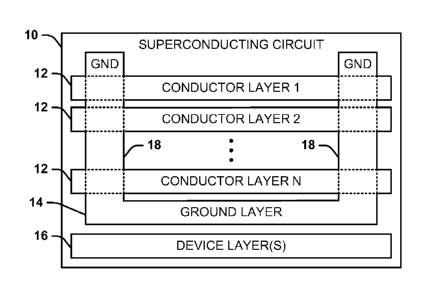
[0016] FIG. 1 illustrates an example of a superconducting circuit 10. The
superconducting circuit 10 can correspond to any of a variety of circuit
components or
portions of a circuit component in a classical, quantum, or combination of
classical and
quantum computing environments. The superconducting circuit 10 includes a
plurality N of
conductor layers 12, where N is a positive integer, a ground layer 14, and at
least one device
3
CA 02960374 2017-03-06
WO 2016/039740 PCMJS2014/055003
layer 16. The device layer(s) 16 can, for example, be associated with
propagating a clock
signal, providing inductive coupling of a signal, such as the clock signal or
other bias signal,
to additional layers, such as in a Reciprocal Quantum Logic (RQL) circuit
implementation,
and/or can include one or more Josephson junctions or other circuit device
component(s).
The conductor layers 12 can each be associated with at least one of signal
routing (e.g., to
and/or from other superconducting circuits), inductive coupling (e.g., between
the conductor
layers 12 or from the device layer(s) 16), and/or at least one Josephson
junction (e.g., as a
JTL). Therefore, the conductor layers 12 can correspond to a wireup for
carrying signals
(e.g., single flux quantum (SFQ) pulses).
[0017] The ground layer 14 can correspond to a coupling to a low-voltage
rail (e.g.,
ground) for providing a ground return path for the signals propagating in the
conductor
layers 12. A physical distance of signal propagation to a ground return path
can correspond
to a source of inductance for a signal in a superconducting computer
environment. Such
inductance can result in reduced signal strength, time delays of signals,
and/or timing
mismatch between multiple signals in the associated quantum computing system.
In the
example of FIG. 1, the superconducting circuit 10 includes a three-dimensional
ground
grid 18 that is conductively coupled to the ground layer 14 and which extends
in a direction
that is orthogonal to the ground layer 14, such that portions of the three-
dimensional ground
grid 18 occupy the conductor layers 12. For example, the portions of the three-
dimensional
ground grid 18 can be patterned from a set of conductors in the conductor
layer to
interconnect respective pairs of vias of the three-dimensional ground grid 18
that extend from
the ground layer 14.
[0018] Therefore, portions of the conductor layers 12 can be used to form
the
respective portions of the three-dimensional ground grid 18 in the same
physical layer to
provide a predetermined measure of control over the inductance of the
respective ground
return path of the signals that propagate in the respective conductor layers
12. As a result, the
superconducting circuit 10 can implement lateral (XY-plane) conductive
coupling to the
associated low-voltage rail (e.g., ground), and can implement vertical (Z-
axis) coupling to
other conductor layers 12. For example, the conductive couplings can have a
substantially
equal distance to the ground connections in this manner to provide an
approximately equal or
predetermined inductance of the signals that propagate in the respective
conductor layers 12.
Such implementation can provide an improved control over the inductance of the
respective
ground return path of the signals that propagate in the respective conductor
layers 12. as
4
CA 02960374 2017-03-06
WO 2016/039740 PCMJS2014/055003
opposed to typical superconducting circuits that include multiple ground
layers that are
interleaved between conductor layers, and which implement vias through holes
in the ground
layer(s) to conductively couple respective conductor layers and vertical
connections to the
respective ground layers for low-voltage rail conductive coupling. For
example, the
superconducting circuit 10 can implement approximately equal inductance ground
return path
connections to provide a more uniform signal response timing for signals
propagating in the
conductor layers 12 (e.g., via JTL connections to and/or from other
superconducting circuits).
[0019] As an example, the superconducting circuit 10 can correspond to a
superconducting circuit cell that can be a portion of an integrated
superconducting circuit.
For example, the three-dimensional ground grid 18 can define a periphery of
the
superconducting circuit cell, such that the three-dimensional ground grid 18
can be formed as
a substantially cage-like structure that substantially encloses circuit
components and signal
elements in the conductor layers 12 and/or the device layer(s) 16. As
described herein, the
term "signal element" refers to one or more conductors on which a signal
(e.g., an SFQ pulse)
can propagate, such as associated with signal routing, an inductor, a
Josephson junction, a
portion of a logic gate, or a variety of other signal-carrying functions.
Thus, an adjacent
superconducting circuit cell can share an adjoining portion of the three-
dimensional ground
grid 18, such as with respect to a pair of vias and/or lateral connecting
horizontal conductors
occupying the conductor layers 12. Therefore, as described herein, the term
"superconducting circuit cell" corresponds to a portion of a superconducting
circuit that
includes at least a portion of a three-dimensional ground grid enclosing at
least a portion of
the superconducting circuit based on vertical vias and horizontal conductors
that conductively
couple pairs of the vias at a periphery of the portion of the superconducting
circuit.
Accordingly, the superconducting circuit cells can be arranged as an array
with shared
portions of the three-dimensional ground grid that define boundaries between
the
superconducting circuit cells. For example, the array of superconducting
circuit cells can
form a superconducting circuit tile that is associated with a superconducting
gate device that
is part of the integrated superconducting circuit. As an example, the gate can
operate as a D-
register, an AND-gate, an inverter, or any of a variety of other types of
logic gates in a
superconducting circuit. Accordingly, the inductance of all conducting signal
portions can be
controlled via conductive couplings to the common three-dimensional ground
grid 18 of each
of the superconducting circuit cells, and thus the superconducting circuit
tile, such as based
on having an approximately equal length conductive coupling to ground.
CA 02960374 2017-03-06
WO 2016/039740
PCMJS2014/055003
[0020] FIG. 2 illustrates an example of a three-dimensional ground grid
system 50.
The three-dimensional ground grid system 50 can correspond in part to the
three-dimensional
ground grid 18 in the example of FIG. 1. Therefore, reference is to be made to
the example
of FIG. 1 in the following description of the example of FIG. 2. As an
example, the three-
dimensional ground grid system 50 can correspond to the three-dimensional
ground grid
structure for a single superconducting circuit cell that forms a portion of a
superconducting
circuit tile.
[0021] The three-dimensional ground grid system 50 includes a three-
dimensional
ground grid 52 that is conductively coupled to a ground layer 54. The three-
dimensional
ground grid 52 includes four vias 56 that each extend along the Z-axis from
the ground
layer 54. The four vias 56 can thus each define an orthogonal corner of a
superconducting
circuit cell. The four vias 56 are conductively coupled via a plurality of
horizontal ground
conductors 58 that extend in the XY plane to couple respective pairs of the
vias 56. The
horizontal ground conductors 58 can correspond to the portions of the three-
dimensional
ground grid 18 that occupy the respective conductor layers 12 in the example
of FIG. 1.
[0022] In the example of FIG. 2, a first oppositely-disposed pair of the
horizontal
ground conductors 58 extends along the Y-axis and occupies a layer
demonstrated at 60. As
an example, the layer 60 can include one or more signal elements that likewise
extend along
the Y-axis between the first oppositely-disposed pair of the horizontal ground
conductors 58
and which corresponds to a first of the conductor layers 12. Similarly, a
second oppositely-
disposed pair of the horizontal ground conductors 58 extends along the X-axis
and occupies a
layer demonstrated at 62. As an example, the layer 62 can include one or more
signal
elements that likewise extend along the X-axis between the second oppositely-
disposed pair
of the horizontal ground conductors 58 and which corresponds to a second of
the conductor
layers 12. Furthermore, a third oppositely-disposed pair of the horizontal
ground
conductors 58 extends along the Y-axis and occupies a layer demonstrated at
64, and a fourth
oppositely-disposed pair of the horizontal ground conductors 58 extends along
the X-axis and
occupies a layer demonstrated at 66. Therefore, the three-dimensional ground
grid 52
extends from the ground layer 54 in a substantially repeated pattern (e.g.,
based on every
other layer).
[0023] As described previously, the three-dimensional ground grid 18 can
define a
periphery of a superconducting circuit cell (e.g., the superconducting circuit
10). In the
example of FIG. 2, the three-dimensional ground grid 52 is demonstrated as a
substantially
6
CA 02960374 2017-03-06
WO 2016/039740 PCMJS2014/055003
cage-like structure which can substantially enclose the signal elements
associated with the
respective conductor layers 12, such that each of the horizontal ground
conductors 58 is
occupies the same layer as the respective signal elements of the conductor
layers 12. Thus,
an adjacent superconducting circuit cell can share a pair of the vias 56 and a
pair of the
horizontal ground conductors 58 (e.g., in either the layers 60 and 64 or the
layers 62 and 66)
with respect to the three-dimensional ground grid that defines the periphery
of the adjacent
superconducting circuit cell. Based on the arrangement of the three-
dimensional ground
grid 52 with respect to the conductor layers 12 that it encloses, the
inductance of the
conductive coupling to the three-dimensional ground grid 52 can be controlled
in each of the
respective superconducting circuit cells in providing ground return paths for
respective
signals propagating in the conductor layers 12.
[0024] FIG. 3 illustrates an example of a superconducting circuit three-
dimensional
wireup system 100. The superconducting circuit three-dimensional wireup system
100 can
correspond to a portion of the three-dimensional ground grid 52 in the example
of FIG. 2,
specifically the horizontal ground conductors 58, and respective signal
elements of the
respective conductor layers. Thus, like reference numbers and reference are
made to the
examples of FIGS. 1 and 2 in the following description of the example of FIG.
3.
[0025] The superconducting circuit three-dimensional wireup system 100
includes the
plurality of horizontal ground conductors 58 associated with the three-
dimensional ground
grid 52, demonstrated as oppositely-disposed pairs in each of the layers 60,
62, 64, and 66.
While the vias 56 are not demonstrated in the example of FIG. 3, it is to be
understood that,
pairs of the vias 56 can be respectively coupled by the horizontal ground
conductors 58,
similar to as demonstrated in the example of FIG. 2. In addition, the
superconducting circuit
three-dimensional wireup system 100 includes a plurality of signal elements
102 that are
associated with the respective conductor layers 12. As an example, the signal
elements 102
can correspond to JTLs along which signals (e.g., SFQ pulses) can propagate.
[0026] In the example of FIG. 3, a first set of the signal elements 102
extends along
the Y-axis between the first oppositely-disposed pair of the horizontal ground
conductors 58,
such that they likewise occupy the layer 60. Similarly, a second set of the
signal
elements 102 extends along the X-axis between the second oppositely-disposed
pair of the
horizontal ground conductors 58, such that they likewise occupy the layer 62.
Furthermore, a
third set of the signal elements 102 extends along the Y-axis between the
third oppositely-
disposed pair of the horizontal ground conductors 58, such that they likewise
occupy the
7
CA 02960374 2017-03-06
WO 2016/039740 PCT/1JS2014/055003
layer 64, and a fourth set of the signal elements 102 extends along the X-axis
between the
fourth oppositely-disposed pair of the horizontal ground conductors 58, such
that they
likewise occupy the layer 66. As a result, in the example of FIG. 3, the
superconducting
circuit three-dimensional wireup system 100 is demonstrated as an XY wireup
with
alternating directions of extension of the signal elements 102 and the
horizontal ground
conductors 58 with respect to the layers 60, 62 64, and 66. As an example, the
horizontal
ground conductors 58 and the signal elements 102 can be patterned separately
from each
other in each of the respective layers 60, 62, 64, 66 during fabrication. For
example, a
common set of conductors in each of the X-axis and the Y-axis can be patterned
to form the
horizontal ground conductors 58 and the signal elements 102 in each of the
respective
layers 60, 62, 64, 66 during fabrication.
[0027] Based on the arrangement of the three-dimensional ground grid 52,
the signal
elements 102 can thus be coupled to the horizontal ground conductors 58 in a
manner that
provides for predetermined control of the inductance of the ground return
paths of the signals
propagating on the signal elements 102. For example, the signal elements 102
can be
coupled to the horizontal ground conductors 58 that occupy the same layer as
the respective
signal elements 102 or can be coupled to horizontal ground conductors 58 in a
layer directly
above or below the layer of the respective signal elements 102, such as based
on a location of
the specific conductor 102 (e.g., with respect to the horizontal ground
conductors 58 on the
same layer). Accordingly, the physical length of the coupling of the signal
elements 102 to
the low-voltage rail (e.g., ground) can be better controlled based on the
arrangement of the
three-dimensional ground grid 52 with respect to the signal elements 102.
[0028] While the example of FIG. 3 demonstrates that each of the layers 60,
62, 64,
and 66 include four signal elements 102, it is to be understood that the
signal elements 102
demonstrate potential locations of the signal elements 102 in each of the
respective
layers 60, 62, 64, and 66. For example, the layers 60. 62, 64, and 66 are not
limited to being
arranged substantially the same (e.g., including four continuous signal
elements 102), but can
be configured in different ways and with a different number or arrangement of
signal
elements 102 with respect to each other based on the arrangement of the
associated
superconducting circuit 10.
[0029] FIG. 4 illustrates an example diagram of a superconducting circuit
cell 150.
The superconducting circuit cell 150 can correspond to a multi-layer
superconducting circuit
8
CA 02960374 2017-03-06
WO 2016/039740 PCMJS2014/055003
cell that can be a portion of a superconducting circuit tile that is
associated with a
superconducting gate.
[0030] In the example of FIG. 4, the superconducting circuit cell 150 is
demonstrated
as a block diagram of a ten layer stack. A first layer 152 is demonstrated as
a clock layer,
such as can be provided a clock signal (e.g., an AC signal or AC quadrature
signal). A
second layer 154 is demonstrated as a bias inductance layer to which the clock
signal can be
inductively coupled to provide a bias current potential for triggering
Josephson junctions
associated with the superconducting circuit cell 150. As an example, the clock
layer 152 and
the bias inductance layer 154 can have portions that are inductively coupled
to provide the
clock signal at at least one polarity to provide sequential triggering of the
respective
Josephson junctions (e.g., in an RQL circuit implementation). Alternatively,
the clock
layer 152 and the bias inductance layer 154 can respectively receive and
induce a DC bias
signal, such as to provide bias for the Josephson junctions for input signals
provided via other
layers of the superconducting circuit cell 150.
[0031] The superconducting circuit cell 150 also includes a ground layer
156 that can
be conductively coupled to a low-voltage rail (e.g., ground), and four
conductor layers
overlying the ground layer 156. The four conductor layers are demonstrated as
a first X-
routing layer 158, a first Y-routing layer 160, a second X-routing layer 162,
and a second Y-
routing layer 164 successively overlying each other. Each of the conductor
layers 158. 160,
162, and 164 can include at least one conductor that extends along the
respective one of the
X-axis (e.g., the conductor layers 158 and 162) or the Y-axis (e.g., the
conductor layers 160
and 164). For example, the conductor(s) in each of the conductor layers 158,
160, 162,
and 164 can be implemented as JTLs to route SFQ pulses to and from other
superconducting
circuit cells. In addition, in the example of FIG. 4, the superconducting
circuit 150 includes a
three-dimensional ground grid 166 that is conductively coupled to the ground
layer 156 and
which extends in a direction that is orthogonal to the ground layer 156 (i.e.,
the Z-axis), such
that portions of the three-dimensional ground grid 166 occupy the conductor
layers 158, 160,
162, and 164, similar to as described previously with respect to the examples
of FIGS. 2-4.
Therefore, the inductance of the conductive coupling to the three-dimensional
ground
grid 166 can be controlled in the superconducting circuit cell 150 in
providing ground return
paths for respective signals propagating in the conductor layers 158, 160,
162, and 164.
[0032] The superconducting circuit cell 150 also includes a Josephson
junction device
layer 168 overlying the second Y-routing layer 164, a first gate inductance
layer 170
9
CA 02960374 2017-03-06
WO 2016/039740
PCMJS2014/055003
overlying the Josephson junction device layer 168, and a second gate
inductance layer 172
overlying the first gate inductance layer 170. The Josephson junction device
layer 168 can
include at least one Josephson junction that can be associated with operation
of a
superconducting gate, such as associated with a superconducting circuit tile
that includes the
superconducting circuit cell 150. Similarly, the first and second gate
inductance layers 170
and 172 can correspond to inductive couplings of signals (e.g., SFQ pulses)
that are provided
to and/or from the superconducting circuit cell 150, such as based on the at
least one
Josephson junction of the Josephson junction device layer 168. Accordingly,
the
superconducting circuit cell 150 can operate as an independent superconducting
circuit or as
part of a larger superconducting circuit (e.g., associated with a
superconducting circuit tile).
[0033] FIG. 5 illustrates another example of a three-dimensional ground
grid
system 200. The three-dimensional ground grid system 200 can include three-
dimensional
ground grides associated with a plurality of superconducting circuit cells
arranged as an
array, such that the three-dimensional ground grid system 200 can correspond
to a
superconducting circuit tile. The three-dimensional ground grid system 200 is
demonstrated
in the example of FIG. 5 in an overhead view (e.g., along the Z-axis).
[0034] The three-dimensional ground grid system 200 includes a ground moat
202
that substantially surrounds at least a portion of a three-dimensional ground
grid 204. The
three-dimensional ground grid 204 can be one integral conductor that is
conductively coupled
to the ground moat 202 and/or to a ground layer (e.g., the ground layer 54)
that can likewise
be coupled to the ground moat 202. The three-dimensional ground grid 204 can
thus include
individual three-dimensional ground grides associated with each of a plurality
of
superconducting circuit cells 206, such that the individual three-dimensional
ground grides
collectively correspond to the overall three-dimensional ground grid 204. In
the example of
FIG. 5, not all of the superconductor circuit cells 206 are demonstrated with
a reference
number for brevity and for clearly demonstrating other components.
[0035] The three-dimensional ground grid 204 includes a plurality of vias
208, a
plurality of X-axis ground conductors 210 that each couple a respective pair
of the vias 208,
and a plurality of Y-axis ground conductors 212 that each couple a respective
pair of the
vias 208. Each of the X-axis ground conductors 210 can be associated with a
separate layer
from the Y-axis ground conductors 212, similar to as demonstrated in the
examples of
FIGS. 2-4. Due to the example of FIG. 5 demonstrating the three-dimensional
ground grid
system 200 in an overhead view, it is to be understood that the three-
dimensional ground grid
CA 02960374 2017-03-06
WO 2016/039740 PCMJS2014/055003
system 200 can be associated with a plurality of layers, such that there can
be a plurality of
X-axis ground conductors 210 and Y-axis ground conductors 212 that
interconnect each pair
of the vias 208. Thus, the three-dimensional ground grid system 200 can
include additional
X and Y-axis ground conductors 210 and 212 located below the demonstrated X
and Y-axis
around conductors 210 and 212.
[0036] Each of the superconducting circuit cells 206 can be arranged
substantially
differently, such as variations of the superconducting circuit 10 and the
superconducting
circuit cell 150 in the examples of FIGS. 1 and 4, respectively. In the
example of FIG. 5,
each adjacent pair of the superconducting circuit cells 206 shares a pair of
the vias 208 and
one or more of the X-axis ground conductors 210 or one or more of the Y-axis
ground
conductors 212. Similar to as described previously, the X-axis ground
conductors 210 and
the Y-axis ground conductors 212 can be arranged to occupy the conductor
layers of each of
the superconducting circuit cells 206, such that signal elements extending
along the X and Y-
axes can extend parallel with and between the X-axis ground conductors 210 and
the Y-axis
ground conductors 212 for each of the superconducting circuit cells 206. As an
example,
each superconducting circuit cell 206 can be associated with a respective
portion of an overall
superconducting circuit of the superconducting circuit tile with which the
three-dimensional
ground grid system 200 is associated. For example, the superconducting circuit
tile that
includes the superconducting circuit cells 206 can be associated with a
superconducting gate,
such as to perform logic functions via SFQ pulses. Therefore, similar to as
described
previously, the inductance of the conductive coupling to the three-dimensional
ground
grid 204 can be controlled in the superconducting circuit tile that includes
the
superconducting circuit cells 206 in providing ground return paths for
respective signals
propagating in the conductor layers of the superconducting circuit cells 206.
[0037] FIG. 6 illustrates an example of a superconducting integrated
circuit 250. The
superconducting integrated circuit 250 can be configured as an integrated
circuit (IC) chip
that includes a superconducting circuit. As an example, the superconducting
integrated
circuit 250 can be fabricated in a manner that is substantially similar to a
complementary
metal-oxide semiconductor (CMOS) fabrication process. In the example of FIG.
6, the
superconducting integrated circuit 250 includes a plurality of superconducting
circuit
tiles 252 arranged in an array of M rows and N columns, where M and N are
positive
integers. For example, each of the superconducting tiles 252 can be associated
with a
separate superconducting gate, such as to perform logic functions in a
quantum, classical, or
11
CA 02960374 2017-03-06
WO 2016/039740 PCT/1JS2014/055003
combination computing system. Each of the superconducting circuit tiles 252
can include a
three-dimensional ground grid system, such as the three-dimensional ground
grid system 200
in the example of FIG. 5. Therefore, each of the superconducting circuit tiles
252 can include
a plurality of superconducting circuit cells, such as the superconducting
circuit cell 150 in the
example of FIG. 4. Thus, each of the superconducting circuit tiles 252 can
have a controlled
inductance for each of the signal elements in respective conductor layers
based on the
arrangement of the associated three-dimensional ground grid system, such as
described
herein.
[0038] What have been described above are examples of the invention. It is,
of
course, not possible to describe every conceivable combination of components
or
methodologies for purposes of describing the invention, but one of ordinary
skill in the art
will recognize that many further combinations and permutations of the
invention are possible.
Accordingly, the invention is intended to embrace all such alterations,
modifications, and
variations that fall within the scope of this application, including the
appended claims.
12