Note: Descriptions are shown in the official language in which they were submitted.
CA 02961685 2017-03-17
1
Description
Injection modulator
The invention relates to an injection modulator for modulating
optical radiation.
For the modulation of optical signals in conjunction with wave-
guides, there are multiple fields of application, such as, for
example, in communication technology, sensor systems, image
transmission, etc. Electro-optical modulators integrated in par-
ticular in semiconductor materials (such as e.g. silicon, InP,
GaAs) play an important part here. Electro-optical modulators,
based on silicon waveguides, are increasingly attracting inter-
est since they constitute a key component for optical broadband
transmission for so-called on-chip, chip-to-chip, fiber communi-
cation, etc. With optical connections it is possible to achieve
significantly higher bandwidths, with moderate energy consump-
tion, compared with the metal-based connections customary here-
tofore.
Various designs are known for light modulator components for
such transmission links. The best known designs are Mach-Zehnder
modulators (Liu et al., Optics Express, 15, 660, 2007), ring
resonators (Xu et al. Nature, 435, 325, 2005) and Fabry-Perot
resonators (Schmidt et al., Optics Express, 16, 334, 2008).
Mach-Zehnder modulators are often used in message transmission
at high data rates. The major advantage of Mach-Zehnder modula-
tors resides in the high optical bandwidth, i.e. the high toler-
ance of the modulators with respect to changes in wavelength of
CA 02961685 2017-03-17
2
the light to be modulated and the high achievable modulation
depth (of the extinction ratio).
In the waveguide-based Mach-Zehnder modulators (Liu et al. Op-
tics Express, 15, 660, 2007), the light passes through an elec-
tro-optical material in at least one arm of the modulator. The
refractive index (or else the absorption) of the electro-optical
material can be varied by applying a voltage. As a result, the
light wave experiences a phase shift in said arm. If the phase
shift is it (or an odd, integer multiple of 7) relative to the
light wave which passes through the other arm of the modulator,
destructive interference occurs at an output of the Mach-Zehnder
modulator when the two waves are superimposed. The modulator may
be operated between states of constructive and destructive in-
terference, also called amplitude modulation. Furthermore, the
modulator structure may also be operated between states of the
same amplitude, but different phases, also called phase modula-
tion. Likewise, it is also possible to switch between combina-
tions of these states. This is generally used to increase the
bits transmittable with a symbol (also higher modulation for-
mats). In order to achieve a phase shift of it, the light has to
pass through a path length, usually in the millimeters to centi-
meters range, in the electro-optical material. Said path length
and thus the minimum structural length of a Mach-Zehnder modula-
tor are dependent on the intensity of the electro-optical ef-
fect.
In order to generate the electro-optical effect, in the semicon-
ductor material regions in or near the waveguide are doped. In
this regard, by way of example, in silicon-on-insulator (SOI)
CA 02961685 2017-03-17
3
waveguides, a p-i-n or else p-n diode structure is produced by
means of doping (Reed et al., Nature Photonics, 4, 518, 2010).
Using such diode structures, the charge carrier concentration in
the waveguides may be varied in a targeted manner. As a result
of the so-called free carrier plasma dispersion effect, this
leads to a variation of the refractive index and of the absorp-
tion behavior in the waveguide (Soref et al., IEEE J. Quant.
Electron., 23, 123, 2004). In this case, by applying a voltage
to the diode in the forward direction, it is possible to inject
charge carriers into the waveguide (referred to as injection)
or, by applying a voltage to the diode in the reverse direction,
it is possible to extract charge carriers from the waveguide
(referred to as depletion).
In electro-optical light modulators according to the "depletion"
principle, the waveguide core itself is p- and/or n-doped. The
light is modulated by a reduction of the charge carriers in the
optical waveguide. It is known that very high modulation speeds
may be achieved by the extraction of the charge carriers in de-
pletion modulators. However, the doping of the waveguide core
leads to a high absorption and thus to high optical losses.
A publication by Z.-Y. Li et al. ( Opt. Express 17, 15947, 2009)
discloses alternating p-and n-doped regions of a p-n diode in a
depletion modulator which can be used to extend the length of
the "depletion zone" in the p-n junction relative to the wave-
guide. As a result, the electro-optical effect may be increased
and the structural size of the modulator may thus be reduced.
The modulation speed of the modulator cannot be increased by
this arrangement.
CA 02961685 2017-03-17
4
An injection modulator having the features according to the pre-
amble of patent claim 1 is known from the publication "CMOS com-
patible fully integrated Mach-Zehnder interferometer in SOI
technology" P. Dainesi et al., IEEE Photonics Technology Let-
ters, Vol. 12, No. 6, June 2000.
The invention is based on the object of specifying an injection
modulator in which it is possible to achieve a fast and large
modulation effect with at the same time comparatively low opti-
cal damping.
This object is achieved according to the invention by means of
an injection modulator having the features as claimed in patent
claim 1. Advantageous configurations of the modulator according
to the invention are specified in dependent claims.
Accordingly, it is provided according to the invention that p-
doped semiconductor portions lie on one side of the waveguide -
as viewed in the longitudinal direction of the waveguide and
relative to the waveguide center -, n-doped semiconductor por-
tions lie on the other side of the waveguide and an intermediate
portion lies in the region of the waveguide center, the semicon-
ductor portions extend in each case transversely with respect to
the waveguide longitudinal direction in the direction of the
waveguide center of the waveguide, and the p-doped semiconductor
portions - as viewed in the longitudinal direction of the wave-
guide - are in each case free of overlap with the n-doped semi-
conductor portions.
A significant advantage of the injection modulator according to
the invention can be seen in the fact that the p-doped semicon-
CA 02961685 2017-03-17
ductor portions and the n-doped semiconductor portions may be
doped relatively highly as a result of their arrangement accord-
ing to the invention, such that it is possible to achieve a rel-
atively strong electro-optical effect in the waveguide. In this
5 case, owing to their overlap-free arrangement, the highly doped
semiconductor portions cause only little additional damping.
The p-doped semiconductor portions and the n-doped semiconductor
portions are preferably respectively electrically connected in
parallel.
Regarding the configuration of the waveguide and the diode
structure, it is considered to be particularly advantageous if
the waveguide is a ridge waveguide comprising a waveguiding ele-
vated ridge portion and two adjacent web portions running paral-
lel to the ridge portion as viewed in the ridge longitudinal di-
rection, the p-doped semiconductor portions are located in one
of the two web portions, the n-doped semiconductor portions are
located in the other of the two web portions, and at least the
center of the ridge portion is free of the p- and n-doped semi-
conductor portions.
With regard to a minimum waveguide damping in the modulation re-
gion, it is considered to be advantageous if the entire ridge
portion is free of the p-and n-doped semiconductor portions.
With regard to a particularly high electric field strength in
the waveguide region, it is considered to be advantageous if the
p-doped semiconductor portions form tine portions of a p-doped
comb structure, the tines of which are arranged at a distance
from one another in the waveguide longitudinal direction and ex-
CA 02961685 2017-03-17
6
tend in each case proceeding from a common contact connection,
located outside the waveguide, from the outside transversely
with respect to the waveguide longitudinal direction in the di-
rection of the waveguide center of the waveguide, and the n-
doped semiconductor portions form tine portions of an n-doped
comb structure, the tines of which are arranged at a distance
from one another in the waveguide longitudinal direction and ex-
tend proceeding from a common contact connection, located out-
side the waveguide, in each case from the outside transversely
with respect to the waveguide longitudinal direction in the di-
rection of the waveguide center of the waveguide.
Preferably, the ridge waveguide comprises a waveguiding layer
and an underlying lower cladding layer. In the case of such a
configuration of the ridge waveguide it is advantageous if the
doping of the n-doped semiconductor portions and that of the p-
doped semiconductor portions extend in each case from the sur-
face of the waveguiding layer of the ridge waveguide as far as
the lower cladding layer.
Preferably, the the width of the p-doped and that of the n-doped
semiconductor portions are in each case smaller than the dis-
tance between adjacent semiconductor portions of the same dop-
ing; such a configuration keeps the waveguide damping in the
waveguide small. Particularly preferably, the ratio between the
width of the semiconductor portions and the distance between ad-
jacent semiconductor portions is less than 1/4.
With regard to the configuration and arrangement of the semicon-
ductor portions it is considered to be advantageous if the p-
doped semiconductor portions form constituents of a first comb
CA 02961685 2017-03-17
7
structure and the n-doped semiconductor portions form constitu-
ents of a second comb structure. The comb spines of the two comb
structures are preferably aligned parallel to the waveguide and
are preferably in each case at a distance from the elevated
ridge portion of the ridge waveguide.
The comb spines preferably in each case are formed by or prefer-
ably at least also comprise a metallic contact connection. Below
the contact connections, the semiconductor material is prefera-
bly likewise doped. Further layers, consisting of suicide, for
example, may be located between the contact connections and the
semiconductor material.
With regard to minimal waveguide losses, it is considered to be
advantageous if the doping in the region of the intermediate
portion is so low that the intrinsic charge carrier density in
the weakly doped or undoped intermediate portion is greater than
the doping in the intermediate portion.
In order to ensure a uniform modulation in the modulation re-
gion, it is considered to be advantageous if the injection modu-
lator is resonator-free and the waveguide overall is reso-
nance-free.
Likewise with regard to a uniform modulation in the waveguide
longitudinal direction, it is considered to be advantageous if
the p-doped semiconductor portions and the n-doped semiconductor
portions - as viewed in the longitudinal direction of the wave-
guide - are arranged offset with respect to one another by half
a distance between adjacent semiconductor portions. In other
words, it is advantageous if at least one of the p-doped semi-
CA 02961685 2017-03-17
8
conductor portions - as viewed in the longitudinal direction of
the waveguide - is arranged centrally between two n-doped semi-
conductor portions lying obliquely opposite, and at least one of
the n-doped semiconductor portions - as viewed in the longitudi-
nal direction of the waveguide - is arranged centrally between
two p-doped semiconductor portions lying obliquely opposite.
In one particularly preferred configuration of the injection
modulator, it is provided that the p-doped semiconductor por-
tions form a p-doped comb structure or constituents thereof and
the n-doped semiconductor portions form an n-doped comb struc-
ture or constituents thereof. The p-doped comb structure is
preferably arranged on one side of the waveguide and the n-doped
comb structure is arranged on the other side of the waveguide.
The tines of the two comb structures are preferably aligned in
each case in the direction of the waveguide center of the wave-
guide. The tines of the p-doped comb structure are free of over-
lap with those of the n-doped comb structure - as viewed in the
longitudinal direction of the waveguide.
The waveguide center, preferably the entire waveguide, is pref-
erably free of tines. In the case of a ridge waveguide, prefera-
bly the entire elevated ridge portion of the ridge waveguide is
free of tines.
Regarding the configuration of the tines, it is considered to
be advantageous if the width of the tines is both at least
four times smaller than the length of the tines and at least
four times smaller than the distance between adjacent tines.
CA 02961685 2017-03-17
9
The waveguide of the injection modulator preferably forms an
MZI (Mach-Zehnder Interferometer) structure. In the case of
such a configuration, it is considered to be advantageous if
at least one of the arms of the MZI structure is equipped with
a diode structure for injecting charge carriers.
Alternatively, the waveguide of the injection modulator may be
arranged in a ring of a ring modulator.
The invention furthermore relates to an arrangement comprising
an injection modulator such as has been described above, and a
radiation source.
In the case of such an arrangement it is advantageous if the
distance between the p-doped semiconductor portions among one
another and the distance between the n-doped semiconductor
portions among one another are in each case greater or less
than half of the wavelength of the radiation of the radiation
source or are greater or less than an integer multiple of said
half. A distance between the semiconductor portions which is
greater or less than half of the wavelength of the radiation
ensures that as a result of the p- and n-doped semiconductor
portions it is not possible for resonance formation to occur
within the modulated waveguide portion and a uniform modula-
tion - as viewed in the waveguide longitudinal direction - is
achieved.
The invention furthermore relates to a method for modulating op-
tical radiation, wherein, with an injection diode structure,
charge carriers are injected into a resonance-free portion of a
waveguide, in which - apart from waveguide damping - the radia-
CA 02961685 2017-03-17
tion intensity of the radiation guided in the waveguide is con-
stant, or previously injected charge carriers are extracted
therefrom.
5 According to the invention, regarding such a method it is pro-
vided that the injection or extraction of holes is performed
from one side of the waveguide and the injection or extraction
of electrons is performed from the other side of the waveguide
by means of a diode structure comprising at least two p-doped
10 semiconductor portions, at least two n-doped semiconductor por-
tions and at least one weakly doped or undoped intermediate por-
tion between the p-doped and n-doped semiconductor portions,
wherein the p-doped semiconductor portions lie on one side of
the waveguide - as viewed in the waveguide longitudinal direc-
tion and relative to the waveguide center -, the n-doped semi-
conductor portions lie on the other side of the waveguide and
the intermediate portion lies in the region of the waveguide
center, wherein the semiconductor portions extend in each case
transversely with respect to the waveguide longitudinal direc-
tion in the direction of the waveguide center of the waveguide,
and
wherein the p-doped semiconductor portions - as viewed in the
longitudinal direction of the waveguide - are both offset and
free of overlap in each case relative to the n-doped semicon-
ductor portions.
Regarding the advantages of the method according to the inven-
tion, reference should be made to the above explanations in
association with the injection modulator according to the in-
vention.
CA 02961685 2017-03-17
11
The invention is explained in greater detail below on the ba-
sis of exemplary embodiments; in the figures here by way of
example:
Figure 1 shows one exemplary embodiment of an injection modu-
lator in which comb structures of an injection diode
structure are arranged outside a waveguide to be
modulated,
Figure 2 shows the injection modulator in accordance with
figure 1 in cross section,
Figure 3 shows one exemplary embodiment of an injection modu-
lator in which the semiconductor portions extend in-
to the waveguide region,
Figure 4 shows the injection modulator in accordance with
figure 3 in cross section,
Figure 5 shows one exemplary embodiment of an injection modu-
lator in which a waveguide that is modulatable by
means of a diode structure forms a Mach-Zehnder in-
terferometer structure,
Figure 6 shows a further exemplary embodiment of an injection
modulator in which an optical waveguide forms a
Mach-Zehnder interferometer structure, wherein both
arms of the interferometer structure are equipped
with a diode structure, and
CA 02 961685 2017-03-17
12
Figure 7 shows one exemplary embodiment of a ring resonator
in which a resonance-free portion of a waveguide is
equipped with a diode structure.
In the figures, the same reference signs are always used for
identical or comparable components, for the sake of clarity.
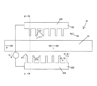
Figure 1 shows an injection modulator 10 comprising an optical
waveguide 20 and a diode structure 30. The diode structure 30
comprises a first comb structure 100, an upper comb structure
in figure 1, for injecting holes and a second comb structure
200, a lower comb structure in figure 1, for injecting elec-
trons.
The first comb structure 100 is equipped with p-doped semicon-
ductor portions 110 extending in the direction of the wave-
guide 20 in finger-shaped fashion proceeding from a comb spine
120. The direction of extent of the p-doped semiconductor por-
tions 110 in the direction of the waveguide 20 is preferably
perpendicular proceeding from the longitudinal direction L of
the comb spine 120 or relative to the longitudinal direction L
of the waveguide 20. The longitudinal direction L of the comb
spine 120 and the longitudinal direction L of the waveguide 20
are preferably parallel. The longitudinal direction L of the
waveguide 20 corresponds to the direction of propagation of
the optical radiation P guided therein.
The p-doped semiconductor portions 110 arranged in a spaced-
apart manner and preferably parallel to one another thus ii-
lustratively form the tines of the comb structure 100, the
CA 02 961685 2017-03-17
13
tips 111 of which serve for injecting holes as soon as the di-
ode structure 30 is activated.
The second comb structure 200 is equipped with n-doped semi-
conductor portions 210 extending in the direction of the wave-
guide 20 proceeding from a comb spine 220 perpendicularly to
the longitudinal direction L of the comb spine 220 and perpen-
dicularly to the longitudinal direction L of the waveguide 20.
The n-doped semiconductor portions 210 are arranged in a
spaced-apart manner and preferably parallel to one another and
serve - during the operation of the diode structure 30 - with
their tips 211 for injecting or extracting holes into or out
of the waveguide 20.
In order to achieve a uniform modulation of the radiation
guided in the waveguide 20, the diode structure 30 is prefera-
bly arranged in a resonance-free portion of the waveguide 20,
in which - apart from waveguide damping - the radiation inten-
sity of the radiation P guided in the waveguide 20 is at least
approximately constant.
Likewise with regard to a uniform modulation of the radiation
P guided in the waveguide 20, in the exemplary embodiment in
accordance with figure 1 it is provided that the p-doped semi-
conductor portions 110 of the first comb structure 100 are
offset relative to the n-doped semiconductor portions 210 of
the second comb structure 200. Preferably, the offset is cho-
sen in such a way that tips 111 of the p-doped semiconductor
portions 110 lie in each case between the tips 211 of the n-
doped semiconductor portions 210 and tips 211 of the n-doped
semiconductor portions 210 lie in each case between assigned
CA 02961685 2017-03-17
14
tips 111 of the p-doped semiconductor portions 110, as is
shown in figure 1.
The comb spine 120 of the first comb structure 100 is prefera-
bly formed by a p-doped semiconductor portion provided wholly
or at least in portions with a metallic contact connection.
The comb spine 220 is correspondingly preferably formed by
n-doped semiconductor material provided wholly or at least in
portions with metallic contact connections.
The injection modulator 10 in accordance with figure 1 can be
operated for example as follows:
In order to inject charge carriers into the region of the
waveguide 20, a forward voltage is applied to the diode struc-
ture 30 by means of a voltage or current source U, as a result
of which, on the part of the p-doped semiconductor portions
110, holes are emitted in the direction of the waveguide 20
and in the direction of the second comb structure 200 and, on
the part of the n-doped semiconductor portions 210, electrons
are emitted in the direction of the waveguide 20 and in the
direction of the p-doped semiconductor portions 110. The holes
and electrons injected into the region of the waveguide 20
modify the refractive index within the waveguide 20, such that
a phase modulation and - on account of the charge carriers -
also a certain damping of the radiation guided in the wave-
guide 20 occur.
If the injected charge carriers are intended to be extracted
as rapidly as possible from the region of the waveguide 20 in
order to bring about a switchover of the modulation, then a
CA 02 961685 2017-03-17
reverse voltage is preferably applied to the diode structure
30, as a result of which the holes and electrons located in
the region of the waveguide 20 are extracted by the first comb
structure 100 and the second comb structure 200.
5
Figure 2 shows the injection modulator 10 in accordance with
figure 1 in a sectional view along the sectional line II-II in
accordance with figure 1.
10 It can be discerned that the waveguide 20 is preferably a
ridge waveguide embodied in a waveguiding layer 21. The wave-
guiding layer 21 is located on a lower cladding layer 22,
which has a smaller refractive index than the waveguiding lay-
er 21 for the purpose of waveguiding in the vertical direc-
15 tion.
For the purpose of lateral waveguiding, the waveguide 20 is
provided with a ridge portion 23 adjoined by two web portions
24 and 25 on the left and right - as viewed in the longitudi-
nal direction of the waveguide. The web height of the web por-
tions 24 and 25 is smaller than the height in the ridge por-
tion 23.
Figure 2 furthermore shows the arrangement of the p-doped sem-
iconductor portions 110 and of the n-doped portions 210. On
account of the sectional plane chosen, only the p-doped semi-
conductor portion 110 is located in the illustrated plane, and
so only this portion is illustrated with a solid line. The n-
doped semiconductor portion 210 is arranged spatially behind
the p-doped semiconductor portion 110 along the chosen viewing
CA 02961685 2017-03-17
16
direction and is therefore illustrated merely with a dashed
line.
In other words, the type of lines chosen in figure 2 is used
to graphically visualize the fact that the p-doped semiconduc-
tor portions 110 and the n-doped semiconductor portions 210
are not located in the same plane, but rather are offset rela-
tive to one another, as has already been mentioned in associa-
tion with figure 1.
In the exemplary embodiment in accordance with figures 1 and
2, with regard to a minimum damping of the radiation guided in
the waveguide 20, the arrangement of the two comb structures
100 and 200 is chosen in such a way that the tips 111 and 211
of the p-doped semiconductor portions 110 and of the n-doped
semiconductor portions 210, respectively, always lie outside
the ridge portion 23 of the waveguide 20.
With regard to injecting electrons and holes as efficiently as
possible, the doping of the p-doped semiconductor portions 110
and that of the n-doped semiconductor portions 210 are chosen
in such a way as to extend down to the lower cladding layer 22
proceeding from the surface 21a of the waveguiding layer 21.
This doping depth ensures that the waveguide 20 can be filled
uniformly with charge carriers in the region of the entire web
height of the web portions 24 and 25.
Figure 3 shows one exemplary embodiment of an injection modu-
lator which corresponds to the injection modulator 10 in ac-
cordance with figures 1 and 2 in terms of construction. In
contrast to the injection modulator in accordance with figures
CA 02 961685 2017-03-17
17
1 and 2, the two comb structures 100 and 200 of the diode
structure 30 are arranged nearer to the waveguide 20. In this
regard, it can be discerned in figure 3 that the tips 111 and
211 of the p-doped semiconductor portions 110 and of the n-
doped semiconductor portions 210, respectively, of the two
comb structures 100 and 200 project right into the waveguide
20. Only the comb spines 120 and 220 of the two comb struc-
tures 100 and 200 are located outside the waveguide 20.
On account of the smaller distance between the p-doped semi-
conductor portions 110 and the n-doped semiconductor portions
210, during operation of the diode structure 30 it is possible
to achieve a greater electric field strength within the wave-
guide 20, a higher modulation speed as a result of faster in-
jection and extraction of previously injected charge carriers,
and also a higher charge carrier density within the waveguide
20. What is disadvantageous is the higher damping of the opti-
cal radiation P in the waveguide 20 that is brought about by
those portions of the p-doped semiconductor portions 110 and
of the n-doped semiconductor portions 210 which project into
the waveguide 20; this is because the tine ends of the two
comb structures 100 and 200 increase the waveguide damping.
In order to minimize the damping, the width b of the semicon-
ductor portions 110 and 210 is chosen to be very much smaller
than the distance A between the semiconductor portions.
For the rest, the explanations in association with figures 1
and 2 correspondingly apply in the case of the exemplary em-
bodiment in accordance with figure 3.
CA 02961685 2017-03-17
18
Figure 4 shows the injection modulator 10 in accordance with
figure 3 along the sectional line IV-IV in cross section. It
can be discerned that the p-doped semiconductor portions 110
and the n-doped semiconductor portions 210 extend right into
the ridge portion 23 of the waveguide 20 proceeding from the
web portions 24 and 25, respectively. A weakly doped or un-
doped intermediate structure 300 nevertheless remains between
the semiconductor portions 110 and 210, said intermediate
structure separating the semiconductor portions from one an-
other and the optical radiation - at least the main part of
the optical radiation - being guided in said intermediate
structure.
In figure 4 it can likewise be discerned that the n-doped sem-
iconductor portions 210 are offset relative to the p-doped
semiconductor portions 110 along the waveguide longitudinal
direction. This is visualized by a dashed line for the n-doped
semiconductor portion 210 in figure 4.
Figure 5 shows one exemplary embodiment of an MZI modulator
400 comprising two interferometer arms 410 and 420. One of the
interferometer arms, for example the interferometer arm 410,
is equipped with an injection modulator 10 such as has been
explained above by way of example in figures 1 to 4.
Once the injection modulator 10 is activated, it is possible
to alter the phase of the radiation guided in the interferome-
ter arm 410 relative to the phase of the radiation guided in
the interferometer arm 420, such that an amplitude modulation
occurs at the output of the MZI modulator 400.
CA 02961685 2017-03-17
19
Figure 6 shows one exemplary embodiment of an MZI modulator
400 in which both interferometer arms 410 and 420 are each
equipped with an injection modulator 10 such as has been ex-
plained above in association with figures 1 to 4.
Figure 7 shows one exemplary embodiment of a ring modulator
500 in which a waveguide 20 forms a ring resonator. An injec-
tion modulator 10 such as has been explained in association
with figures 1 to 4 is provided in a resonator-free portion of
the waveguide 20. The explanations above thus correspondingly
apply to the modulator 10 in accordance with figure 7.
Although the invention has been more specifically illustrated
and described in detail by means of preferred exemplary embod-
iments, nevertheless the invention is not restricted by the
examples disclosed and other variations can be derived there-
from by the person skilled in the art, without departing from
the scope of protection of the invention.
CA 02 961685 2017-03-17
List of Reference Signs
10 Injection modulator
20 Waveguide
5 21 Layer
21a Surface
22 Cladding layer
23 Ridge portion
24 Web portion
10 25 Web portion
Diode structure
100 Upper comb structure
110 P-doped semiconductor portion
111 Tips
15 120 Comb spine
200 Lower comb structure
210 N-doped semiconductor portion
211 Tips
220 Comb spine
20 300 Intermediate portion
400 MZI modulator
410 Interferometer arm
420 Interferometer arm
500 Ring modulator
A Distance
b Width
L Longitudinal direction
P Optical radiation
U Voltage/current source