Note: Descriptions are shown in the official language in which they were submitted.
CA 02961842 2017-03-20
WO 2016/046061
PCT/EP2015/071350
Transparent conductive layer, a film comprising the layer, and a process for
its production
Description
The present invention relates to a transparent conductive layer comprising non-
conductive are-
as and conductive areas. The invention further relates to a patterned
transparent conducting
film comprising the layer and a process for producing such a film.
Patterned transparent conductive films comprising a transparent conductive
layer are used for
example in flat liquid crystal displays, touch panels, electroluminescent
devices, thin film photo-
voltaic cells, as anti-static layers, and as electromagnetic wave shielding
layers.
The transparent conductive layers generally are composites, comprising an
optically transparent
contiguous solid phase and a conductive network of electroconductive
nanoobjects which ex-
tend throughout the solid phase. The solid phase, also referred to as matrix,
is formed of one
ore more optically transparent polymers. The matrix binds the
electroconductive nanoobjects
within the layer, fills the voids between the electroconductive nanoobjects,
provides mechanical
integrity and stability to the layer and binds the layer to the surface of the
substrate. The con-
ductive network of electroconductive nanoobjects allows for flow of an
electric current between
adjacent and overlapping electroconductive nanoobjects within the layer. Due
to the small di-
mensions of the nanoobjects, their influence on the optical behavior of the
composite is quite
small thus allowing for the formation of an optically transparent composite,
i.e. a composite hav-
ing a light transmission of 80% or more in the visible region (400 to 700 nm)
measured accord-
ing to ASTM D 1003.
A transparent conductive layer and a process for its production are disclosed
for example in
WO-A 2013/095971. For producing a transparent electrically conductor an
electrically conduc-
tive layer is disposed onto a transparent substrate. The electrically
conductive layer comprises a
plurality of interconnecting metallic nanowires and a polymeric overcoat
layer. In the electrically
conductive layer a pattern is formed, wherein the pattern comprises
electrically conductive are-
as which are separated by electrically insulating traces. The traces are
produced by irradiation
with a laser, wherein material of the electrically conductive layer is
removed. Therefore, the
traces are formed as valleys in the electrically conductive layer. The valleys
have a depth in the
range from 10 to 100 nm and a cross-sectional width in the range from 10 to
1000 pm. The val-
leys further comprise a plurality of crevices having a depth in the range from
50 to 100 nm.
Further transparent conductive layers comprising a polymer matrix and
conductive nanowires
are disclosed in US-A2007/0074316 or US-B 8,018,568. In the conductive areas
the nanowires
interconnect. The non-conductive areas are formed by etching or photo-
patterning by using
photocurable matrix materials.
CA 02961842 2017-03-20
WO 2016/046061
PCT/EP2015/071350
2
However, etching the non-conductive areas has the disadvantage that multistep
wet chemistry
has to be used. Further, as well as in photo-patterning, the pattern may be
visible. A disad-
vantage of the process as disclosed in WO-A 2013/095971 is that metal of the
nanowires is
vaporized and re-deposited on the edges of the spots irradiated by the laser,
forming highly re-
flective dots or circles of tens of microns sizes. Therefore, there may be
significant changes in
haze, transparency and reflectance in the irradiated regions which means that
the pattern also
may be visible.
A further disadvantage of all known processes is that it is not possible to
produce a smooth sur-
face due to the production processes.
Therefore, it is an object of the present invention to provide a transparent
conductive layer in
which the pattern is not visible and which further has a smooth surface. It is
a further object of
the present invention to provide a patterned transparent film and a process
for producing such a
transparent conductive film.
This object is achieved by a transparent conductive layer comprising non-
conductive areas and
conductive areas, wherein the conductive areas comprise an interconnected
network of electri-
cally conductive nanoobjects and in the non-conductive areas the nanoobjects
are converted
into particles and wherein the thickness of the conductive areas and the non-
conductive areas
differs less than 10 nm.
In regard to the present invention the term "particles" means spheres or short
segments of the
nanowires into which the nanowires have been converted.
The invention further relates to a patterned transparent conductive film,
comprising a substrate
and the conductive layer on the substrate.
To achieve a transparent conductive film, the substrate onto which the ink is
applied is optically
transparent. The substrate preferably is made of glass, polycarbonate,
polyethylene tereph-
thalate, cyclic olefin polymer, polyimide, or polymethyl methacrylate.
In accordance with the present invention, the nanoobjects which have been
converted into par-
ticles in the non-conductive areas remain in the layer, wherein the particles
generated during
conversion remain at the same position at which the nanowires have been. This
has the ad-
vantage that it is not necessary to remove material from those parts of the
transparent conduc-
tive layer which form the non-conductive areas. Therefore, the optical
characteristics of the
conductive areas and the non-conductive areas are similar to a large extend.
The conductive areas and the non-conductive areas are defined by their sheet
resistance. The
sheet resistance is a measure of resistance of a sheet namely uniform in
thickness. The term
CA 02961842 2017-03-20
WO 2016/046061
PCT/EP2015/071350
3
"sheet resistance" implies that the current flow is along the plane of the
sheet, not perpendicular
to it. For a sheet having a thickness t, a length L and a width W, the
resistance R is
R=p= L --p = ¨L =Rsh = -L
W=t t W W
wherein Rsh is the sheet resistance. Accordingly the sheet resistance Rsh is
W
Rsh = R=¨.
L
In the formula given above, the bulk resistance R is multiplied with a
dimensionless quantity
(W/L) to obtain the sheet resistance Rsh, thus the unit of sheet resistance is
Ohm. For the sake
of avoiding confusion with the bulk resistance R, the value of the sheet
resistance is commonly
indicated as "Ohm per Square" because in the specific case of a square sheet
applies W=L and
Rsh=R. The sheet resistance is measured for example by means of a four point
probe.
In a preferred embodiment, the ratio of sheet resistance in the non-conductive
areas and the
conductive areas is larger than 1000. In a particular preferred embodiment,
the ratio of sheet
resistance in the non-conductive areas and the conductive areas is larger than
10000. The
sheet resistance of the non-conductive areas preferably is larger than 100,000
ohms per square
(OPS), more preferred larger than 1,000,000 OPS, and particularly larger than
10,000,000 OPS.
The sheet resistance of the conductive areas preferably is smaller than 1000
OPS, more pre-
ferred in the range from 5 to 500 OPS, and particularly in the range from 10
to 100 OPS.
In a preferred embodiment, the difference in light transmission of the non-
conductive areas and
the conductive areas is less than 5 %. Particularly preferred, the difference
in light transmission
of the non-conductive areas and the conductive areas is less than 0.5 %. The
light transmission
refers to the percentage of an incident light which is transmitted through a
medium. The light
transmission of the conductive areas according to the invention is at least 80
%, measured ac-
cording to ASTM D 1003 (Procedure A). More preferred, the light transmission
is at least 85 %,
further preferably at least 90 % and particularly preferably at least 95 %, in
each case measured
according to ASTM D 1003 (Procedure A).
The difference in haze of the non-conductive areas and the conductive areas
preferably is less
than 0.5 %. Particularly preferred the difference in haze is less than 0.01 %.
The haze of the
conductive areas of the transparent conductive layer is preferably 2 % or
less, more preferably
1.8 % or less, further preferably 1.5 % or less and particularly preferably
1.2 %, in each case
measured according to ASTM D 1003 (Procedure A).
The measurement of haze and light transmission (in ASTM D 1003 referred to as
luminous
transmittance which is the ratio of the luminous flux transmitted by a body to
the flux incident
upon it) by means of a hazemeter is defined in ASTM D 1003 as "Procedure A ¨
Hazemeter".
CA 02961842 2017-03-20
WO 2016/046061
PCT/EP2015/071350
4
The values of haze and light transmission (corresponding to the luminous
transmittance as de-
fined in ASTM D 1003) given in the context of the present invention refer to
this procedure.
Generally haze is an index of the light diffusion. It refers to the percentage
of the quantity of light
separated from the incident light and scattered during transmission. It is
typically caused by sur-
face roughness, and by embedded particles or compositional heterogeneities in
the medium.
According to ASTM D 1003, in transmission, haze is the scattering of light by
a specimen re-
sponsible for the reduction in contrast of objects viewed through said
specimen, i.e. the percent
of transmitted light that is scattered so that its direction deviates more
than a specified angle
(2.5 ) from the direction of the incident beam.
A nanoobject in regard to the present invention is an object having one, two,
or three external
dimensions in the nanoscale, i.e. in the size range from approximately 1 nm to
100 nm. The
electrically conductive nanoobjects to be used for the present invention are
electrically conduc-
tive nanoobjects having two external dimensions in the range from 1 nm to 100
nm and their
third external dimension in the range from 1 pm to 100 pm. Typically, said two
external dimen-
sions which are in the range from 1 nm to 100 nm are similar, i.e. they differ
in size by less than
three times. The third dimension of the electrically conductive nanoobjects is
significantly larger,
i.e. it differs from the other two external dimensions by more than three
times. Such nanoobjects
also are referred to as nanofibers.
The electrically conductive nanoobjects used in the present invention are
preferably nanowires
or nanotubes. Nanowires are electrically conductive nanofibers, nanotubes are
hollow nano-
fibers.
Electrically conductive nanoobjects used for the present invention typically
have a cross section
close to circular shape. Said cross section extends perpendicularly to said
external dimension
which is in the range of from 1 pm to 100 pm. Thus, said two external
dimensions which are in
the nanoscale are defied by the diameter of said circular cross section. Said
third external di-
mension extending perpendicular to said diameter is referred to as the length.
Preferably, the electrically conductive nanoobjects have a length in the range
from 1 pm to
100 pm, more preferably from 3 pm to 50 pm, and particularly preferably from
10 pm to 50 pm.
The diameter of the electrically conductive nanoobjects preferably is in the
range from 1 nm to
100 nm, more preferably from 2 nm to 50 nm, particularly preferably from 3 nm
to 30 nm.
To provide a sufficient electrical conductivity, the electrically conductive
nanoobjects are made
of a metal or carbon. Preferably, the electrically conductive nanoobjects are
made of silver,
copper, gold, platinum, palladium, nickel or carbon. In case the electrically
conductive nanoob-
jects are made of a metal, preferably silver, copper, gold, platinum,
palladium or nickel, the na-
noobjects preferably are nanowires. In case the electrically conductive
nanoobjects are made of
CA 02961842 2017-03-20
WO 2016/046061
PCT/EP2015/071350
carbon, the nanoobjects preferably are nanotubes. Particularly preferably, the
nanoobjects are
silver nanowires, gold nanowires or copper nanowires, particularly silver
nanowires.
In the conductive areas of the transparent conductive layer, the nanoobjects
are interconnected.
5 The amount of nanoobjects is such that the interconnecting nanoobjects
are in contact. Due to
the contact of the nanoobjects, electric current can flow in the conductive
areas. On the other
hand, in the non-conductive areas the nanoobjects are converted into
particles. The particles
are not in contact with each other and therefore, no electric current can
flow. The particles, into
which the nanoobjects have been converted, have a cross section which
corresponds to the
cross section of the nanoparticles. The diameter of the cross section of the
particles is in the
range from 1 to 100 nm, preferably in the range from 2 to 50 nm. The length of
the particles is in
the range from 1 nm to 1 pm, preferably in the range from 2 nm to 500 nm.
To provide a transparent conductive layer, the nanoobjects are embedded in a
transparent ma-
trix. Matrix materials are generally transparent polymers, for example
hydropropyl methyl cellu-
lose, crystalline cellulose, poly(meth)acrylates, copolymers of acrylates and
methacrylates,
copolyers of styrene and (meth)acrylates, carboxymethyl cellulose, poly
acrylamide, polyvinylal-
cohol, polyvinylpyrrolidone, polystyrenesulfonic acid, dextran or blends
thereof.
The further object of the invention is achieved by a process for producing a
patterned transpar-
ent conductive film, comprising:
(a) applying of an ink comprising electrically conductive nanoobjects and a
binder on a sub-
strate, forming a layer;
(b) drying the layer;
(c) patterning the layer by irradiating with a laser, the pattern
comprising conductive areas
and non-conductive areas, wherein in the non-conductive areas the conductive
nanoob-
jects are converted into particles.
The ink, which is applied on the substrate, comprises electrically conductive
nanoobjects as
described above, a binder and generally additionally a solvent.
Suitable electrically conductive nanoobjects are known in the art and are
commercially availa-
ble.
Nanowires made of metals, for example silver nanowires, are typically
commercially available in
the form of an aqueous dispersion wherein polyvinylpyrrolidone is adsorbed
onto the surface of
the nanowires in order to render the dispersion stable. Any matter adsorbed on
the surface of
the nanowires is not included in the above-defined dimensions and composition
of the electrical-
ly conductive nanoobjects.
CA 02961842 2017-03-20
WO 2016/046061
PCT/EP2015/071350
6
The binder which is comprised in the ink forms the matrix of the transparent
conductive layer by
drying. To provide an ink, which can be applied to the substrate, the solvent
is selected such
that the binder is soluble in the solvent. As the nanowires are not soluble,
the nanowires are
dispersed in the solvent comprising the solved binder. The binder corresponds
to the matrix
material of the transparent conductive layer as defined above and is
preferably selected from
the group consisting of hydropropyl methyl cellulose, crystalline cellulose,
poly(meth)acrylates,
copolymers of acrylates and methacrylates, copolyers of styrene and
(meth)acrylates, carboxy-
methyl cellulose, poly acrylamide, polyvinylalcohol, polyvinylpyrrolidone,
polystyrenesulfonic
acid, dextran or blends thereof.
In case the binder is a poly(meth)acrylate, a copolymer comprising
(meth)acrylate, for example
a copolymer of acrylate and methacrylate, or a copolymer of styrene and
(met)acrylate, the sol-
vent preferably is water. Herein, the term "(meth)acrylate" includes
"acrylate" and "methacry-
late".
However, if polymers are used as binder which are not soluble in water, the
solvent preferably is
an organic solvent. Preferably, the solvent is selected from the group
consisting of water, alco-
hols, ketones, ethers, hydrocarbons or aromatic solvents. Suitable aromatic
solvents are for
example benzene, toluene ore xylene. Particularly preferred, however, the
binder is selected
from polymers which are water soluble and the solvent is water.
The ink which is applied to the substrate preferably comprises 0.01 to 1 wt%,
preferably 0.05 to
0.5 wt% electrically conductive nanoobjects, 0.02 to 5 wt%, preferably 0.1 to
1.5 wt% binder and
solvent.
As an alternative or additionally, the ink comprises a binder which is
dispersed in the solvent. In
this case the binder is in form of particles of a polymer having a number
average molecular
weight of 25000 g/mol or higher. The dispersed particles have a mean diameter
in the range
from 10 nm to 1000 nm.
In a further alternative embodiment, the binder comprises fibers of
crystalline cellulose dis-
persed in water. The fibers of crystalline cellulose have a length in the
range from 80 nm to
300 nm and a diameter in the range from 5 nm to 30 nm.
Besides poly(meth)acrylate, a copolymer comprising (meth)acrylate, for example
a copolymer of
acrylate and methacrylate, or a copolymer of styrene and (met)acrylate, the
binder may com-
prise as an alternative or additionally one or more water-soluble polymers
selected from the
group consisting of hydroxypropyl methyl cellulose, carboxymethyl cellulose,
polyacrylamide,
polyvinylalcohol, polyvinylpyrrolidone, polystyrenesulfonic acid and dextran.
CA 02961842 2017-03-20
WO 2016/046061
PCT/EP2015/071350
7
Each of the above identified binders can be used as a single binder or in
combination with at
least one further binder. For example a mixture of poly(meth)acrylate or a
(meth)acrylate com-
prising copolymer and crystalline cellulose can be used.
A suitable ink is disclosed for example in US application No. 62/037630 and US
application No.
62/037635.
To apply the ink onto the substrate, any suitable printing process can be
used. In a preferred
embodiment, the ink comprising conductive nanowires and binder is applied by
spin coating,
draw down coating, roll-to-roll coating, gravure printing, microgravure
printing, screen-printing,
flexoprinting and slot-die coating.
Preferably, the ink is applied to the surface of the substrate in a thickness
in a range of from 1
pm to 200 pm, preferably of from 2 pm to 60 pm. The thickness is also referred
to as "wet thick-
ness" and relates to the state before removing the liquid constituents of the
ink by drying. At a
given target thickness (after removing the liquid constituents of the
composition as explained
above) and accordingly a given target sheet resistance and light transmission
of the electrocon-
ductive layer to be prepared, the wet thickness may be the higher the lower
the concentration of
solid constituents in the composition is in the ink. The process of applying
the ink is facilitated
when there is no need to use a particular low wet thickness.
After applying the ink to the substrate, the layer which is formed by applying
the ink is dried to
remove solvent and to achieve a solid layer. The solid layer which is formed
from the ink by dry-
ing preferably has a thickness in the range from 10 nm to 1000 nm, preferably
from 50 nm to
500 nm.
The drying of the layer preferably is carried out at a temperature in the
range from 20 to 200 C
for 0.5 to 30 min. Particularly preferably the drying is carried out at a
temperature in the range
from 100 to 150 C. The duration of the drying process particularly preferably
is in the range
from 1 to 15 min.
The temperature at which the drying process is carried out depends on the
solvent used, the
melting point of the nanowires and the coating process. For silver nanowires,
the upper limit is
about 200 C. If a solvent is used which evaporates easily, a lower
temperature, for example
ambient temperature, can be used. On the other hand, a higher temperature for
drying the layer
has to be used in case the solvent does not evaporate at low temperatures or
only a small
amount of the solvent evaporates. To accelerate the drying process, the drying
preferably is
carried out at higher temperatures of at least 100 C. However, when the ink is
applied to the
substrate by roll-to-roll coating such as gravure printing, flexoprinting and
slot-die coating, the
drying of layers may be carried out in ambient conditions.
CA 02961842 2017-03-20
WO 2016/046061
PCT/EP2015/071350
8
The duration of the drying process depends on the drying temperature. The
duration is selected
such that at the end of the drying process the residual moisture content in
the ink is below a
defined value. To achieve the desired residual moisture content, the duration
of evaporation
increases with decreasing temperature for the same solvent.
In case water is used as a solvent, generally the drying is carried out at a
temperature in the
range from 100 to 150 C for a duration of 1 to 15 min.
The atmosphere in which the drying is carried out is preferably selected such
that no chemical
reaction takes place between any component of the atmosphere and the ink. The
atmosphere in
which the drying of the layer is carried out preferably comprises air,
nitrogen or noble gases, for
example argon. Particular preference is given to air or nitrogen.
After applying the ink and drying of the layer, a pattern of conductive areas
and non-conductive
areas is formed in the layer by irradiation with a laser. The operating
conditions of the laser are
selected such that the electrically conductive nanoobjects are converted into
particles and that
as little as possible material of the layer evaporates. By this operating
conditions the material of
the layer remains in the layer and the differences in thickness, light
transmission and haze be-
tween conductive areas and non-conductive areas are as small as possible.
The laser which is used to convert the electrically conductive nanoobjects can
be any laser
which allows the conversion of the nanoobjects into particles. Suitable lasers
are for example IR
laser or UV laser. Preferably, the laser which is used in the process is a
fiber laser. The laser
can be operated in pulsed mode or continuous wave mode.
The pattern comprises non-conductive lines and conductive areas which are
surrounded by the
non-conductive lines. The width of the non-conductive lines preferably is in
the range from 10 to
1000 pm, particularly in the range from 50 to 500 pm.
By forming the non-conductive areas by irradiation with a laser in such a form
that the electrical-
ly conductive nanoobjects are converted into particles and remain in the
conductive transparent
layer, the differences in thickness between the non-conductive areas and the
conductive areas
are in the range from 1 to 10 nm, particularly in a range from 2 to 5 nm. Due
to the small differ-
ences in thickness of the conductive areas and the non-conductive areas, a
smooth surface of
the conductive transparent layer can be achieved. This smooth surface also
helps in invisible
patterning and any subsequent processes that require planarization.
The differences in haze and light transmission of the conductive transparent
layer and the pat-
terned conductive transparent film which is produced by the above process are
as described
above.
CA 02961842 2017-03-20
WO 2016/046061
PCT/EP2015/071350
9
The invention is hereinafter further illustrated by means of examples. Results
additionally are
shown in the figures.
In the figures:
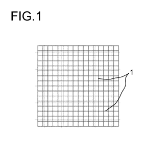
Figure 1 shows a grid pattern;
Figure 2(a) shows an optical image with a rectangle indicating AFM scanned
area;
Figure 2(b) shows an AFM height image at 100 pm x 100 pm;
Figure 2(c) shows AFM profile analysis.
Figure 3 shows a SEM image of a laser treated silver nanowire layer;
Figure 4 shows a detail of the laser treated silver nanowire layer of
figure 3.
Examples
Example 1: Preparation of silver nanowire layers on glass substrates
Hydropropyl methyl cellulose is dissolved in water at a concentration of 1
wt%. The dissolved
hydropropyl methyl cellulose and a dispersion of silver nanowires in water
(0.5 wt%) are mixed
in water so that the final concentration of silver nanowires is 0.25 wt% and
the mass ratio of
hydropropyl methyl cellulose and silver nanowires is 1:2, respectively.
Nanowires are obtainable
for example from Seashell Technologies (San Diego, CA). The mixture is spin
coated on glass
substrates at 2000 rpm for 30 sec. The layers are then dried at 130 C for 5
min. The sheet re-
sistance is measured by a 4 point probe station (Lucas lab pro-4) and the
optical properties are
measured by BYK haze gard plus.
Example 2: Preparation of silver nanowire layers on polycarbonate substrates
A styrene acrylic copolymer aqueous solution with 35% solid content, available
as Joncryl 60
by BASF SE, is diluted in water to a concentration of 20 wt%. A copolymer of 2-
ethylhexyl acry-
late methyl methacrylate, available as Acronal LR9014 by BASF SE is diluted
in water to a
concentration of 10 wt%. A dispersion of silver nanowires in water (0.5 wt%),
the diluted styrene
acrylic copolymer aqueous solution and the diluted copolymer of 2-ethylhexyl
acrylate methyl
methacrylate are mixed in water so that the final concentration of the silver
nanowires is 0.4
wt% and the mass ratio of styrene acrylic copolymer, copolymer of 2-ethylhexyl
acrylate methyl
methacrylate and silver nanowires is 4:3:3, respectively. The mixture is ball
milled for 3 min to
CA 02961842 2017-03-20
WO 2016/046061
PCT/EP2015/071350
achieve homogenization. A conductive layer is printed on an optical
polycarbonate foil, for ex-
ample commercially available under the product specification Makrofol DE 1-1
175 pm from
Bayer Material Science, using a draw-down bar (wet thickness t=6pm, coating
speed v=2"/sec)
was dried for 5 min at 135 C. Sheet resistance and optical properties are
measured as in Ex-
5 ample 1.
Example 3: Laser patterning of silver nanowire layers on glass ¨ grid pattern
10 A silver nanowire layer prepared according to example 1 is patterned by
laser according to a
grid pattern as shown in figure 1. The laser is a Rofin model F20 operating
at I = 1070 nm,
pulse repetition rate 60 kHz, and laser power 3W. The width of the focused
beam on the sub-
strate was about 30 pm. The distance between adjacent lines is 1.5 mm. The
laser was
scanned across the substrate at a speed of about 600 mm/sec. The patterned
layer is examined
under scanning electron microscope (SEM). The SEM images are shown in figures
3 and 4,
wherein figure 4 shows the detail which is marked by the rectangle in figure
3.
The laser traces 1 are roughly 30 pm wide. The silver nanowires 5 in the non-
treated regions 4
are intact while those in the laser traces 1 are converted to silver particles
6. The particles 6
have similar diameters to the silver nanowires 5 and they stay where the
nanowires were before
the laser treatment.
Figure 2(a) shows an optical image with a rectangle indicating a 100 pm x 100
pm AFM
scanned area. Figures 2(b) and 2(c) show the AFM height image and profile
analysis, wherein
figure 2(b) shows the detail which is marked by a rectangle in figure 2(a).
The red triangles in
figures 2 (b) and 2(c) indicate the two locations where the height of the film
was measured. As
can be seen in figure 2(c), the thickness of the conductive areas and the non-
conductive areas
differs by 3.8 nm.
Example 4: Optical property change of silver nanowire layers on glass after
laser treatment
In order to measure the optical property change after laser treatment, silver
nanowire layers on
25 cm-by-25 cm size are prepared according to example 1 on glass and the
entire surface is
processed by laser. An Infrared fiber laser is used. The incident laser energy
is varied by using
different laser power, pulse repetition rate and velocity. After laser
treatment, the sheet re-
sistance is measured as in example 1. The results are shown in tables 1.1 and
1.2.
CA 02961842 2017-03-20
WO 2016/046061
PCT/EP2015/071350
11
Table 1.1:
Sample Laser Pulse rep- Velocity Rsh Rsh
power etition rate (mm/s) before after
(W) (Hz) (OPS) (OPS)
1 3 90k 600 84 3 -1000
2 3 80k 600 77 3 co
3 3 70k 600 81 1 co
4 3 50k 600 74 5
3 90k 550 81 1 co
6 3.2 90k 600 77 6
Table 1.2:
Sample # T T after AT % H H after A H
before (/o) before (/o)
(0/0) (0/0)
1 92.1 91.7 0.4 0.75 0.75 -0
2 92.0 91.5 0.5 1.04 1.03 0.01
3 92.1 91.3 0.8 0.83 0.85 0.02
4 92.0 89.4 0.6 0.84 0.96 0.12
5 92.1 91.6 0.5 0.83 0.82 0.01
6 92.1 91.6 0.5 0.87 0.90 0.03
5
Samples 1 through 4 are treated with the same laser power and velocity but
different pulse rep-
etition rate. Lower pulse repetition rate leads to higher incident laser
energy. Sample 1 shows a
sheet resistance (Rsh) of about 1000 OPS indicating the incident laser energy
is too low to break
down the percolating network completely. Samples 2 and 3 show a sheet
resistance which ex-
ceeded the measurement range and was too high to be measured. The optical
properties
change very little after the laser treatment, satisfying the requirements. The
incident laser ener-
gy for sample 4 is higher. As a result, the transmission T and the haze H
change is also higher
(2.6% and 0.12%, respectively).
Samples 5 and 6 are treated with the same pulse repetition rate as sample 1
but with different
velocity and laser power, respectively. Lower velocity or higher laser power
leads to higher inci-
dent laser energy. Therefore, both sample 5 and 6 have higher incident laser
energy than sam-
CA 02961842 2017-03-20
WO 2016/046061
PCT/EP2015/071350
12
ple 1. Both samples show no conductance and the optical properties change very
little after the
laser treatment, satisfying the requirements.
Example 5: Optical property change of silver nanowire layers on polycarbonate
after laser
treatment
A sheet of silver nanowire layer on polycarbonate is prepared according to
example 2. In order
to measure the optical property change after laser treatment, a piece of 25cm-
by-25cm size is
cut and the entire surface of this piece is processed by the laser. After
laser treatment, the
sheet resistance is measured as in example 1. Results are shown in Tables 2.1
and 2.2.
Table 2.1:
Sample Laser Pulse rep- Velocity Rsh Rsh
power etition rate (mm/s) before after
(W) (Hz) (OPS) (OPS)
7 2 100k 2000 58 3
Table 2.2:
Sample T T after AT% H H after AH %
before (/o) before (/o)
(cm (0/4
7 90.3 89.4 0.9 1.16 1.14 0.02
At this incident laser energy, sample 7 shows no conductance and and optical
properties
change very little after the laser treatment , satisfying the requirements.